國 立 交 通 大 學
光電工程研究所
博 士 論 文
低溫多晶矽薄膜電晶體元件特性
應用於光感測器之研究
Study on Characterization of Low-Temperature
Poly-Silicon Thin Film Transistor for
Optical Sensor Application
研 究 生 : 郭 彥 甫
指導教授 : 戴 亞 翔 博士
低溫多晶矽薄膜電晶體元件特性
應用於光感測器之研究
Study on Characterization of Low-Temperature
Poly-Silicon Thin Film Transistor for
Optical Sensor Application
研 究 生: 郭 彥 甫
Student:
Yan-Fu
Kuo
指導教授: 戴 亞 翔 博士
Advisor:
Dr.
Ya-Hsiang
Tai
國 立 交 通 大 學
光電工程研究所
博 士 論 文
A Dissertation
Submitted to the Institute of Electro-Optical Engineering
Department of Photonics College of Electrical and Computer Engineering
National Chiao Tung University
in Partial Fulfillment of the Requirements
for the Degree of
Doctor of Philosophy
in Electro-Optical Engineering
September 2010
Hsinchu, Taiwan, Republic of China
i
低溫多晶矽薄膜電晶體元件特性
應用於光感測器之研究
研 究 生: 郭 彥 甫
指導教授: 戴 亞 翔 博士
國 立 交 通 大 學
光電工程研究所
摘要
本論文探討低溫多晶矽薄膜電晶體元件特性應用於光感測器之研究。由於在 薄膜電晶體的SPICE 電路模型中,並沒有對應的光漏電流模型可供模擬;同時, 傳統定義暗態電流與照光電流比例的光敏感性參數並不適合用作分析光漏電機 制。因此,本論文首先提出以Unit-Lux-Current (ULC) 參數來分析元件的光效應 行為。此參數反應的是單位光通量致光電流的能力並且與元件的暗態電流無關。 光漏電流的成因是由於空間電荷區產生額外的載子所致。根據加諸於半導體的電 場導致庫倫位障降低的 Poole-Frenkel 效應與聲子共振穿隧效應;在橫向空乏區 與閘極-汲極重疊空乏區產生的光漏電流行為以及與活化能相關的溫度等效應, 都有詳細於文中所提出的物理模型與能帶圖解釋探討。而後也提出此光漏電參數 的相關場效應與溫度效應的方程式去進一步研究其光漏電機制。 接著本論文也探討光效應與直流偏壓所額外產生不均勻缺陷的關係。由於矽 材料能帶結構是屬於非直接能隙,根據動量守恆原理,矽材料吸收光所產生過多 的電子-電洞對無法在價電帶與傳導帶直接複合,而是傾向透過能隙間的缺陷態ii 作複合的動作。我們研究直流偏壓狀態下多晶矽薄膜電晶體主要的兩大劣化機 制,熱載子效應與自發熱效應,這樣的劣化所導致的光漏電流亦會嚴重影響我們 在設計感測電路時的困難度。當光照在經過熱載子劣化後的元件,在空乏區域裡 的多數電子-電洞對從這些因熱載子劣化而額外存在的淺態能階(Tail state)中產 生。而當元件經過自發熱劣化後,矽薄膜層因高溫釋放氫造成斷鍵而形成了深態 能階(Deep state),而又因為此能階分佈在能隙的中間處,對矽材料來說,它同時 也提供了照光產生電子-電洞對最有效率的複合中心。在本論文中我們利用這兩 種劣化情況去探討因缺陷所導致的相關光漏電行為,同時也修改缺陷非勻狀態的 薄膜電晶體所對應的光漏電方程式。這些經驗方程式的建立將有助於模型化與模 擬低溫多晶係薄膜電晶體電路操作在直流偏壓劣化後的光效應行為分析。 接下來由於低溫多晶矽薄膜電晶體是上閘極結構,操作時它同樣會受到來自 高強度環境背光源的影響而導致光漏電流的發生。基本上能夠採用正面照光的方 式分析背面照光的光漏電流。然而不同的是,當光的來源為背光時,會有大量的 電子-電洞對產生在元件多晶矽薄膜層的底部。因此將會有殘留過量的電洞累積 因而形成正電位通道。在本文中我們同樣也探討背光致光漏電流的各式偏壓效 應、溫度以及缺陷密度等影響因子。同時,我們利用缺陷在能階的分佈與背光導 致電流關係的新觀點進一步去確認先前研究所未見之自發熱效應淺態能階的存 在與位置,進而建立元件完整且正確的劣化模型。 本論文最後也提出了低溫多晶矽薄膜電晶體自我閘極遮蔽的三維嵌入光偵 測的概念。這個系統利用了光源相對閘極汲極側與閘極源極側的正反向量測來建 立感測方向,因而提供元件在照光下感測的不匹配特性。由於此概念並未改變元 件製作流程,是可以期待整合至面板的偵測系統的。接者提出利用低溫多晶矽薄 膜電晶體設計的一個源極隨耦態的電路去做環境光的感測。同時各種可能產生的 元件變動性被考慮並利用統計性與補償電路的方式校正,此系統同樣也有著能整 合至面板偵測系統的潛力。
iii
Study on Characterization of Low-Temperature
Poly-Silicon Thin Film Transistor for
Optical Sensor Application
Student:
Yan-Fu
Kuo
Advisor:
Dr.
Ya-Hsiang
Tai
Department of Photonics & Institute of Electro-optical Engineering,
College of Electrical and Computer Engineering
National Chiao Tung University
Abstract
This work focuses on the characterization of low-temperature poly-silicon thin film transistor for sensor application. Due to in the SPICE models of TFT, there is no photo leakage current model for simulation. Meanwhile, photosensitivity (RL/D)
defined as the ratio of the current under illumination to the current in the dark is not proper to be used to analyze photo leakage mechanism. Thus, a new parameter, Unit-Lux-Current (ULC) is firstly used to analyze the effects of illumination on LTPS TFTs. It reflects the ability of photo leakage current induced per unit-photo flux and independent of the dark current. The amount of the photo current should be associated with the carrier generation in the space charge region. Based on the Poole-Frenkel effect lowering of a Coulombic barrier and phonon-assisted tunneling due to the electric field applied to a semiconductor, the ULC can be taken into account both the
iv
leakage current induced in the lateral depletion and in the gate-drain overlap depletion regions. We further take into account the temperature effect of ULC. The temperature effect can be identified by activation energy. An equation is provided to properly describe model for mechanism ULC behavior under various bias and temperature conditions for further exploration of photo leakage mechanism.
Then we focus on the relation between photosensitivity and additional non-uniform defects. The energy-band structure of Si material is indirect band-gap. The excess electron-hole pairs induced by the absorption of light would not be recombined from band to band directly due to the momentum conservation principle. Thus silicon is more likely to recombine through localized traps. We investigate the two main degradation mechanisms for the poly-Si TFTs under DC operation, namely the hot carrier effect and the self heating effect. Due to such degradation, the photo-induced leakage current is strongly influenced which is difficultly designed for sensing circuits. When the LTPS TFT devices after hot carrier stress are under optical illumination, the numerous electron-hole pairs from additionally created shallow tail states are generated in the lateral depletion region. Then devices after self heating stress, the high temperature in the poly-Si film can release hydrogen and cause plenty of dangling bonds as deep states. These deep states near mid level, in the lateral depletion region, can recombine the electron-hole pairs generated by irradiation. In this work, we apply both stress conditions deliberately to manipulate the defect-related photo behaviors and modify ULC equations in TFTs. The empirical equation of ULC provides a potential modeling for simulation of LTPS TFT circuitry considering the photo effect after DC stress.
Next, because LTPS TFTs are top gate structure, it is suffer from undesirable photo leakage current under a high back illumination environment. We can analyze such photo-induced current like as front light case. However, when the light is emitted
v
from back-light, plenty of electron-hole pairs are generated in the bottom of poly-Si film. Therefore, the residual excess holes are accumulated in the poly-Si film to form the floating body with a positive channel potential. We also present detail studies on the factors that affect the photo leakage current like bias condition, temperature, and defect states of the LTPS TFTs. Meanwhile, we provide new insight which use energy level of trap defect behaviors connected with photo induced current to further make sure the existence of tail state after self heating degradation. Furthermore, a more accurate model after self-heating degradation is proposed.
A three dimensional embedded optical sensor employs low temperature poly-silicon thin film transistor which used gate metal shielding by itself characteristics was proposed. The system connect with forward and reverse measurements can be used to set up sensing direction. It provides sensing disparity characteristics of adopted devices under illumination. It’s expected the integration of sensing system onto the panel without extra components sensors and extra change in the fabrication process. Then a circuit of source follower type based on the LTPS TFTs which can sense the illumination condition is proposed to be used as an ambient light sensor. Some kinds of variation effect can be calibrated by statistical and compensation circuit methods. This approach would provide the possibility for the light sensor array integrated in the pixels with the same device of LTPS TFTs.
vi
誌謝
執筆至此,求學之路即將抵達一個終站,回顧求學歷程的點滴,心中真的是 百感交集。在交大博士班修業的這些年裡,首先我想感謝我的指導教授戴亞翔博 士。由於老師的用心指導與耐心協助,讓我受益良多並且不斷成長,在研究路上 因而走得更平穩踏實,進而順利完成論文。除此之外,也感謝老師在生活上的貼 心鼓勵,設身處地體諒與包容學生遇到的困難,教導自己如何看待、度過人生中 所面對的波折,在這裡要先對老師致上誠摯的謝意。另外,也要感謝張鼎張及劉 伯村兩位教授在專業領域上的指導與協助,兩位老師積極的態度與對研究的熱 忱,讓我獲益匪淺,對學生的關心與幫助,同樣也是讓我倍感窩心。還有論文口 試委員的趙天生、黃乙白和莊敏宏教授於百忙之中前來給予指導,提供許多寶貴 的意見,讓我的論文能夠更趨完善。 接著要感謝實驗室的弘緯、震鑠及興華學長,和曾經一起同甘共苦的夥伴 們,同實驗室的士哲、隔壁實驗室的皓彥、一德和士欽,感謝大家的鼓勵協助與 彼此打氣,讓我在研究上感到迷惑時能找到方向,能繼續擁有研究的熱忱以及挑 戰夢想的堅持;也要感謝實驗室學弟妹:允翔、枷彬、漢清、國珮、騰瑞、紹文 在過去所提供的幫助;祿盛和志融,讓我後期的資料能夠順利完成。以及其他的 碩士班學弟妹,感謝過去曾和大家共同度過的歡樂時光。還有好友嘉軒的支持與 鼓勵,旭銘、天浩、文化、沈謙等好友的陪伴,讓我在忙碌的研究生活中,增添 許多歡笑的色彩,豐富了我的生活,謝謝你們帶給我的每個精彩與回憶。 最後,這一刻的喜悅我想獻給我摯愛的父母,感謝我的父母多年來辛苦的栽 培與教誨,總是在背後默默的支持我、適時給予我關心、鼓勵與肯定,給我力量 完成學業。能夠完成這篇論文,我由衷地感謝我的家人。 僅將此文獻給所有我愛的師長、家人與好友 彥甫 2010 誌於風城交大vii
Contents
Chinese Abstract --- i
English Abstract --- iii
Acknowledgment --- vi
Contents --- vii
Figure Captions --- ix
Table Captions --- xv
Chapter 1 Introduction
1.1 General Background --- 01 1.2 Motivation --- 02 1.3 Thesis Organization --- 04Chapter 2 Experimental
2.1 Device Fabrication --- 11 2.2 Experimental Procedures --- 122.3 Extraction Methods of Device Parameters --- 13
Chapter 3 Photosensitivity Analysis of Low-Temperature Poly-Si
Thin Film Transistor Based on Unit-Lux-Current
3.1 Introduction --- 193.2 Classification and Characterization of Photosensitivity --- 20
3.3 Insight of Photosensitivity --- 22
3.4 Conclusion --- 26
Chapter
4 Dependence of Photosensitive Effect on the Defects
Created by DC Stress for LTPS TFTs
4.1 Introduction --- 454.2 Electrical Degradation of Poly-Si TFT under DC Stress --- 46
4.3 Insight of Defect-Related Photosensitivity --- 48
viii
Chapter 5 Investigation of Backlight Sensing in Poly-Si TFTs
5.1 Introduction --- 71
5.2 Experimental Procedures --- 72
5.3 Results and Discussions --- 72
5.4 Conclusion --- 79
Chapter 6 Characterization of Thin film Transistor for Optical
Sensor Application
6.1 Three-Dimension Poly Silicon Interaction Display --- 1016.2 Sensing Circuits of Source Follower Type using LTPS TFTs ---- 103
6.3 Light Sensor for Detecting Uniformity of Backlight Intensity -- 111
6.4 Conclusion --- 112
Chapter 7 Conclusions and Suggestions for Future Work
--- 133References ---
135Vita ---
147ix
Figure Captions
Chapter 1
Fig. 1-1 (a) Model for the crystal structure of polysilicon films. (b) The charge distribution within the crystallite and at the grain boundary. (c) The energy band structure of the polysilicon crystallites. --- 06 Fig. 1-2 Three possible mechanisms of leakage current in poly-Si TFTs, including
thermionic emission, thermionic field emission and pure tunneling. ---- 07 Fig. 1-3 The poly-Si density of states distribution. --- 08 Fig. 1-4 The figure illustrating the structure of this dissertation. --- 09
Chapter 2
Fig. 2-1 The cross-section views of n-channel LTPS TFTs with LDD structure. -- 15 Fig. 2-2 The photo leakage current and the power variation spectrum of the light
source. --- 16 Fig. 2-3 Emission spectrum of a phosphor-based white LED. --- 17
Chapter 3
Fig. 3-1 Photograph of the special U-shaped TFT with an arrow indicating the scanning path of the illumination beam. --- 28 Fig. 3-2 The drain current of the U-shaped TFT with the distance that the
illumination beam scanning along the channel direction. --- 29 Fig. 3-3 The ID-VG transfer characteristics under illumination from dark to 31320
x
Fig. 3-4 Gate bias dependence of LTPS TFT photo currents and dark currents in off
region. --- 31
Fig. 3-5 The relationship between leakage current and illumination intensity under different bias conditions. --- 32
Fig. 3-6 Gate bias effect on Unit-Lux-Current at different drain biases. --- 33
Fig. 3-7 Drain bias effect on Unit-Lux-Current at different gate biases. --- 34
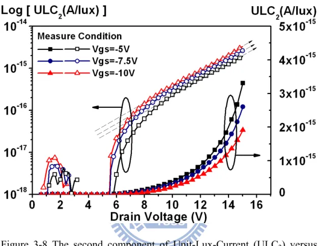
Fig. 3-8 The second component of Unit-Lux-Current (ULC2) versus drain bias at different gate voltages. --- 35
Fig. 3-9 The calculated and experimental data of drain bias effect on Unit-Lux Current at different gate biases. --- 36
Fig. 3-10 Temperature effect on photo leakage current of LTPS TFT. --- 38
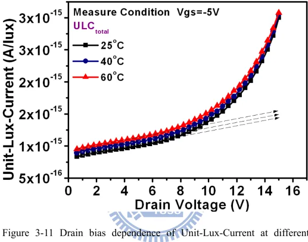
Fig. 3-11 Drain bias dependence of Unit-Lux-Current at different temperatures. --- 39
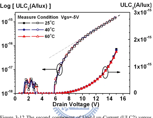
Fig. 3-12 The second component of Unit-Lux-Current (ULC2) versus drain bias with different temperatures. --- 40
Fig. 3-13 Dependence of factors α and β on temperatures. --- 41
Fig. 3-14 A proposed model of ULC mechanism for LTPS TFT. --- 42
Fig. 3-15 Photo leakage current variation among different devices. --- 43
Chapter 4
Fig. 4-1 The profile of Joule heat generated in the channel for the device under self heating stress. --- 55Fig. 4-2 The comparison for the heat transfer coefficients of the films for the poly-Si TFTs. --- 56
xi
Fig. 4-3 The Ids-Vgs transfer characteristics under different illumination conditions
for (a) conventional LDD and (b) only one-side LDD device structures.--- -- 57 Fig. 4-4 The Ids-Vgs transfer characteristics with 1V drain voltage before and after
(a) hot carrier stress and (b) self heating stress under different illumination conditions. --- 58 Fig. 4-5 (a) Normalized Unit-Lux-Current and mobility at Vds=0.6V and 10V with
hot carrier stress times. (b) Normalized ULC and threshold voltage at Vds=0.6V and 10V with self heating stress times. --- 59
Fig. 4-6 Drain bias effect on Unit-Lux-Current with different hot carrier stress times.--- 60 Fig. 4-7 (a) The first component (ULC1) and (b) the second component (ULC2) of
Unit-Lux-Current versus drain bias with different hot carrier stress times.--- 61 Fig. 4-8 Dependence of fitting factors A1.A2 and B1, B2 on hot carrier stress. --- 62
Fig. 4-9 Drain bias effect on Unit-Lux-Current with different self heating stress times.--- 63 Fig. 4-10 (a) The first component (ULC1) and (b) the second component (ULC2) of
Unit-Lux-Current versus drain bias with different self heating stress times.--- 64 Fig. 4-11 Dependence of fitting factors A1.A2 and B1, B2 on self heating stress. --- 65
Fig. 4-12 A proposed hot carrier degradation model of ULC mechanism for TFTs.--- 66 Fig. 4-13 The photo leakage current spectrum of the light source in the range of
350-750 nm at lower bias after hot carrier stress. --- 67 Fig. 4-14 A proposed self heating degradation model of ULC mechanism for
xii
TFTs.--- 68 Fig. 4-15 The photo leakage current spectrum of the light source in the range of
350-750 nm at lower bias after self heating stress. --- 69
Chapter 5
Fig. 5-1 The cross section of device under back light illumination. --- 81 Fig. 5-2 The transmission rate and absorption rate of LED light source. --- 82 Fig. 5-3 Distribution of electron-hole pairs in the poly-Si of TFTs. --- 84 Fig. 5-4 The Explanation of current flow of poly-Si under back light
illumination.--- 85 Fig. 5-5 Relationship between leakage current and illumination intensity under
different bias conditions. --- 86 Fig. 5-6 (a) Drain bias effect on Unit-Lux Current at different gate biases. (b) Gate
bias effect on Unit-Lux Current at different drain biases. --- 87 Fig. 5-7 Experiment data (symbols) and empirical formula (solid lines). --- 88 Fig. 5-8 Drain bias dependence of Unit-Lux Current at different temperature. ---- 90 Fig. 5-9 Iillum measured at Vgs=-5V, Vds=3V dependence on the illumination
intensity before and after 1000 seconds of hot carrier or self heating stress with (a) forward and (b) reverse measurements. --- 92 Fig. 5-10 Drain bias dependence of ULC at different hot carrier stress times
measured in the forward mode.--- 93 Fig. 5-11 Drain bias dependence of ULC at different hot carrier stress times
xiii
Fig. 5-12 The Ids-Vgs transfer characteristics of TFTs with (a) forward and (b) reverse
measurements in saturation region 5V drain voltage under different back illumination conditions for self heating stress. --- 95 Fig. 5-13 Drain bias dependence of ULC at different self heating stress times
measured in the forward mode.--- 96 Fig. 5-14 Drain bias dependence of ULC at different self heating stress times
measured in the reverse mode. --- 97 Fig. 5-15 The normalized (a) gate-to-drain capacitance Cgd and (b) gate-to-source
capacitance Cgs curves before and after stress with different
--- 98 Fig. 5-16 The cross section views of degradation model in TFT structure under hot
carrier and self heating stress conditions. --- 99
Chapter 6
Fig 6-1 The ID-VG transfer characteristics under illumination from dark to 31320
lux. (Figure insert) rotatable probe station experimental setup. --- 113 Fig 6-2 Gate metal shielding by itself for poly-Si TFTs. --- 114 Fig 6-3 The forward and reverse measured photo currents verses negative gate bias
with several incident angles under (a)5100 lux (b)20500 lux illumination conditions. --- 115 Fig 6-4 Forward and reverse photo currents ratio verses incident angles under 5100
lux and 20600 lux illumination conditions. --- 116 Fig 6-5 Using LTPS TFTs as oblique light sensors for three dimensional
interaction display (a) Single light source (b) Multiple light sources. -- 117 Fig 6-6 Schematic diagram of proposed 2T1C light sensing circuit and its timing
xiv
Fig 6-7 Illumination dependence of ID-VD characteristic and its fitting
formula.--- 119 Fig 6-8 SPICE simulation results of TFT (W/L=20um/5um). --- 121 Fig 6-9 (a) The modified 2T1C light-sensing circuit model for simulation (b) its
time diagram. --- 122 Fig 6-10 Simulation results under illumination and in the dark. --- 123 Fig 6-11 The comparison of the current ratio of under illumination and in the dark
RL/D among on, subthreshold, and off region and that of current level
(inset). --- 124 Fig 6-12 Measured waveforms of output voltages of proposed 2T1C light-sensing
circuit illuminative variations from dark to 31320 lux on (a) subthreshold region and (b) off region. --- 125 Fig 6-13 Measured output slopes of fifteen proposed light-sensing circuits in off
region (dash line) and their average curve (solid line). --- 126 Fig 6-14 The influence of Vth shift operated on (a) subthreshold region (b) off
region. --- 127 Fig 6-15 Average slopes versus illumination intensity with five samples as an
average unit. --- 128 Fig 6-16 (a) Schematic of our proposed light-sensing circuit with compensation part and (b) time diagram. --- 129 Fig 6-17 Fifty times of Monte Carlo simulation results of the proposed 2T1C
light-sensing circuit when Vth shift is ±0.5V (a) before compensation (b)
after compensation. --- 130 Fig 6-18 (a) Simplified block diagram of digitization circuit and (b) its signal
xv
Table Captions
Chapter 3
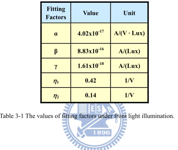
Table 3-1 The values of fitting factors under front light illumination. --- 37
Chapter 5
Table 5-1 The drain bias and gate bias effects on photo leakage for LTPS TFTs. --- 83 Table 5-2 The values of fitting factors under back light illumination. --- 89 Table 5-3 The values of temperature fitting factors under back light
illumination.--- 91 Table 5-4 The defect information of several analyses.--- 100
Chapter 6
Table 6-1 I0(L) and R0=1/A0(L) at VGS=0.5V with the illumination intensity variation.
1
Chapter 1
Introduction
1.1 General Background
Thin film transistor (TFT) is a metal-oxide-silicon field effect transistor (MOSFET) fabricated on an insulator substrate which are included glass substrates, flexible substrates and so on by employing all thin film constituents. Thin film transistors have been widely used as switching devices in flat panel display, such as active-matrix liquid crystal display (AMLCD) [1.1-1.4] and active-matrix organic light emitting diode (AMOLED) display [1.5-1.9]. As for the active region material, it can be mainly divided into amorphous silicon (a-Si) and poly-crystalline silicon (poly-Si) types. The hydrogenated a-Si (a-Si:H) TFT is commonly applied in large size active matrix displays (AMDS) due to its highly mature process, low manufacturing cost and good device uniformity. However, the low electron field effect mobility of a-Si TFTs limits the capability of advanced and integrated circuit. On the contrary, polycrystalline silicon thin-film transistors (poly-Si TFTs) have attracted much attention because of their widely applications. Compare with a-Si:H TFTs, poly-Si TFT can provide higher electron mobility and its higher driving current allows smaller TFT size to be used as the pixel-switching elements, resulting in higher aperture ratio and lower parasitic gate-line capacitance for improved display performance. It offers a promising solution to realize the “System on Panel” technology. Nevertheless, using excimer laser to re-crystalline a-Si active layer, poly-Si TFT can offer very high current capability. However, the laser re-crystallization process also generates plenty
2
of the grain boundaries in poly-Si TFT, leading to poor uniformity and very huge variation due to the narrow laser process windows for producing large grain size poly-Si TFT. The fluctuation of pulse-to-pulse laser energy and non-uniform laser beam profile make laser energy density hard to hit the super lateral regime everywhere. The random grain boundaries and traps exist in the channel region [1.10-1.12]. This will cause serious non-uniformity of brightness in AMOLED panel. Since the device-to-device uniformity is hard to control, it is essential to develop circuits to compensate the variation. The roadmap for the poly-Si TFTs are expected that as the mobility and the device performance keeps improving, the driver circuits and some special value-added functions can be formed by the use of poly-Si TFTs eventually form the system on glass (SOG) technology. This somehow proved that for the display electronics the poly-Si TFTs can replace the externally connected bond ICs and the perspective of the SOG technology is truly applicable.
1.2 Motivation
The poly-Si TFT technology has some distinct advantages but its manufacture is more complex and high cost. The major advantage of poly-Si TFT is the higher field effective mobility than that of the amorphous silicon (a-Si) based devices. The high carrier mobility and the existence of complementary pairs permit the integration of drive circuits and the smaller area of pixel transistor. The integration of drive circuits could reduce manufacturing costs, and increase the functionality of large-area microelectronics [1.13-1.14]. The smaller area of pixel transistor leads to a larger aperture ratio for a given pixel size, or enables a high resolution display for a given aperture ratio, resulting in fine image quality for mobile display. Recently, the demand
3
of high-end mobile electronic products such as cell phone, digital camera, GPS, mobile TV and so on is continuing to grow, so that the development of mobile displays with high resolution and high image quality is inevitable. Since most of people would like to use mobile electronic products outdoors under the sunlight, the readability in ambient illumination is a critical issue for mobile displays. To meet the requirement of superior readability under sunlight, the brightness of backlight becomes higher and higher. However, poly-Si TFTs operated in the high illumination environment exhibit substantial photo leakage current and degraded sub-threshold swing (S.S.), leading to the errors of gray level and difficulty in pixel design.
In addition, the application of circuit integration using poly-Si TFT continuously grow up as device characteristics improve further. Enlarging the grains in poly silicon layers is an effective approach for improving TFT performance. Several poly-Si re-crystallization methods based on laterally grown grains have been proposed to enlarge the grains and control the location of the grain boundaries [1.15-1.16]. In poly-Si TFT devices, however, the status of defect states at grain boundaries plays a crucial role for electrical characteristics, as shown in Fig. 1-1 and Fig. 1-2. Meanwhile, Fig. 1-3 shows the poly-Si density of states distribution. Shallow tail states are associated with strained bonds and deep states near mid-gap are associated with broken bonds. The stability of poly-Si TFT is one of the important issues for poly-Si technology. Recently, the researches about the stabilities of conventional excimer laser crystallized (ELC) poly-Si TFTs have been reported. The creation of trap states at poly-Si/gate dielectric interface or the charge trapping in the gate insulator is responsible for the degradation in electrical characteristics of poly-Si TFTs.
In this thesis, the photosensitive effect of n-type low temperature polycrystalline silicon thin-film transistors is investigated. A new index Unit-Lux-Current (ULC) characterizing the slope of the curve is introduced to discuss the photosensitivity. It is
4
discovered that the device photosensitivity is dependent on the gate, drain bias and temperature. Furthermore, we further use a peculiar device to demonstrate that the photo leakage current occurs in the depletion region at the drain junction. A qualitative deduction is developed to account for the photo leakage mechanism. However, the poly-Si TFTs suffer from several degradation mechanisms, such as hot carrier and self-heating effects. It was discovered that the photo-generated carrier behaviors under optical illumination are related to defect types created by different stress conditions. A model considering the relation between photosensitivity and defect is proposed to explain the anomalous illumination behaviors after device degradation. The empirical equation of ULC provides a potential modeling for simulation of LTPS TFT circuitry considering the photo effect. In addition, AMLCD requires back-light source to display input image. Poly-Si TFT operated in back illumination environment exhibits an undesired high leakage current to affect the function of pixel switch. The photo behaviors of poly-Si under back light illumination are also studied in detail. We also proposed three dimensional embedded optical sensors employs low temperature poly-silicon thin film transistor which used gate metal shielding by itself. This system provides sensing disparity characteristics of adopted devices under illumination. Meanwhile, we also proposed source follower type circuits to make ambient light sensors. Both applications are expected that the integration of sensing system onto the panel without extra novel device process development.
1.3 Thesis Organization
In this thesis, the photo behaviors of low-temperature polycrystalline silicon thin film transistors (poly-Si TFT) under front and back light illumination were studied. Furthermore, the models of electrical characteristics of poly-Si TFT under
5
illumination were investigated and established in detail. In addition, the photo leakage behaviors after DC stress degradation are also examined. Meanwhile, several optical sensor applications were developed in this work.
This dissertation is divided into seven chapters. It can be summarized in Fig. 1-4. The dissertation is organized in to the following chapters: In chapter 1, the general background and overview of low temperature polycrystalline silicon thin-film transistors are introduced. In chapter 2, the experimental, such as the fabrication and the measurement of the devices, is described. In chapter 3, photosensitivity analysis of low-temperature poly-Si thin film transistor based on Unit-Lux-Current is investigated. In chapter 4, dependence of photosensitive effect on the defects created by DC stress for LTPS TFTs is studied. In chapter 5, investigation of backlight sensing in Poly-Si TFTs is presented. In chapter 6, characterization of thin film transistor for optical sensor application is studied. Finally, the summarization of all experimental results in this dissertation and the suggestions for the future work are presented in chapter 7.
6
Figure 1-1 (a) Model for the crystal structure of polysilicon films. (b) The
charge distribution within the crystallite and at the grain boundary. (c)
The energy band structure of the polysilicon crystallites.
7
Figure 1-2 Three possible mechanisms of leakage current in poly-Si TFTs,
including thermionic emission, thermionic field emission and pure
tunneling.
1 2 3 2 1 3 Ec Ev EtLeakage Current Mechanism (1) Thermionic emission (2) Thermionic field emission (3) Pure tunneling
8
9
11
Chapter 2
Experimental
2.1 Device Fabrication
The process flow of TFTs is described below. Top gate LTPS TFTs with width/length dimension of 20µm/5µm were fabricated using low temperature process. Firstly, the buffer oxide and a-Si:H films with thickness of 50 nm were deposited on glass substrates with PECVD. The samples were then put in the oven for dehydrogenation. The XeCl excimer laser of wavelength 308 nm and energy density of 400 mJ/cm2 was applied. The laser scanned the a-Si:H film with the beam width of 4 mm and 98% overlap to recrystallize the a-Si:H film to poly-Si. After poly-Si active area definition, 100 nm SiO2 was deposited with PECVD as the gate insulator. Next,
the metal gate was formed by sputter and then defined. For n-type devices, the lightly doped drain (LDD) and the n+ source/drain doping were formed by PH3 implantation
with dosage 2 × 1013 cm-2 and 2 × 1015 cm-2 of PH3 respectively. The LDD
implantation was self-aligned and the n+ regions were defined with a separate mask. The LDD structure did not use on p-type devices. The p+ source/drain doping was done by B2H6 self-align implantation with a dosage of 2 × 1015 cm−2. Then, the
interlayer of SiNX was deposited. Subsequently, the rapid thermal annealing was
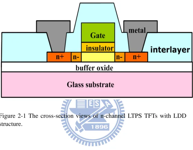
conducted to activate the dopants. Meanwhile, the poly-Si film was hydrogenated. Finally, the contact hole formation and metallization were performed to complete the fabrication work. The structure cross section view for the n-type poly-Si TFT is given in Fig. 2-1.
12
2.2 Equipment and Experiment Setup
In this section, the equipments to measure the device characteristics, namely the transfer behavior ID-VG curves and the capacitance curves, are described. In addition,
the apparatus to DC stress the device is also illustrated. The ID-VG curves for the
devices are measured by the Agilent 4156A precision semiconductor parameter analyzer. The C-V curves of the gate-to-source capacitance CGS and gate-to-drain
capacitance CGD before and after stress with different frequencies are measured with
the HP 4284A precision LCR meter. Before measuring the capacitance behavior, for every frequency the measure correction is performed with the open-circuit and short-circuit mode respectively for the needles before and after probing the electrode to eliminate the effect of the parasitic components in the surrounding and during probing. The DC stress is performed by the Agilent 4156A precision semiconductor parameter analyzer, which is the same one to measure the transfer characteristics.
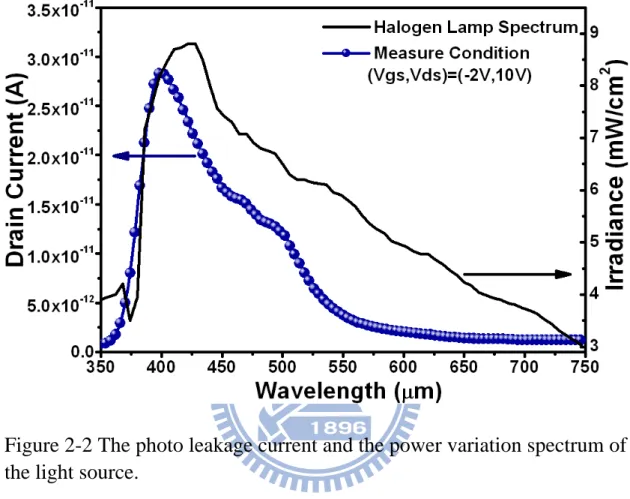
The light was collimated and focused onto the device with top face white light illumination. Photo leakage current was induced by a halogen lamp irradiation stream with several neutral density filters (light intensity ranging from dark to 31320 lux) through the objective of a microscope, and the light intensity was measured by a digital luminous flux meter. Fig. 2-2 shows the photo leakage current, the power variation spectrum of the front light source in the range of 350-750nm.
The light was collimated and focused onto the device with bottom face white light illumination. However, compare with front light source we use halogen lamp irradiation, we use white light-emitting-diode (LED) as the back light source in our experiments. The white light LED backlight spectrum in the range of 350-750nm is also shown as Fig. 2-3.
13
2.3 Extraction Methods of Device Parameters
Three important device parameters are extracted and studied in this work: the threshold voltage VTH, the sub-threshold swing S.S., and the field effect mobility μFE.
Plenty methods are used to determine VTH, which may be the most important
parameter in application. In most of the researches on TFT, the constant current method is adopted. In this work the threshold voltage is determined by this method, which extract VTH from the gate voltage at the normalized drain current ID=10 nA for
VD=0.1V.
Sub-threshold swing S.S. (V/dec), is also a typical parameter to describe the control ability of gate toward channel. The sub-threshold swing should be ideally independent of drain voltage and gate voltage. However, in reality, the sub-threshold swing might increase with drain voltage due to short-channel effects. It might as well be affected by the serial resistance and interface traps and therefore become related to the gate voltage. In this work, it is defined as the minimum amount of gate voltage required to increase drain current by one order of magnitude.
The field effect mobility, μFE, is determined from the maximum transconductance
gm at low drain voltage, which in this work 0.1 V is used. The transfer characteristics of poly-Si TFTs are similar to those of conventional MOSFETs, so the first order the first order I-V relation in the bulk Si MOSFETs can be applied to the poly-Si TFTs, which can be expressed as ]
2 1 ) [( 2 D D TH G ox FE D V V V V L W C I =μ − − , where Cox is the
gate oxide capacitance per unit area, W is channel width, L is channel length, VTH is
the threshold voltage. If the drain voltage VD is much smaller compared with
(VG-VTH), then the ID can be approximated as D FE ox VG VTH VD
L W C
14
the electron field effect mobility can be expressed as m D ox FE g WV C L = μ ,where the transconductance is defined as D FE ox const V G D m V L WC V I g D μ = ∂ ∂ = | = .
15
Figure 2-1 The cross-section views of n-channel LTPS TFTs with LDD
structure.
16
Figure 2-2 The photo leakage current and the power variation spectrum of
the light source.
17
19
Chapter 3
Photosensitivity Analysis of Low-Temperature Poly-Si Thin Film
Transistor Based on Unit-Lux-Current
3.1 Introduction
Low temperature polycrystalline silicon (LTPS) thin film transistors (TFTs) have attracted much attention for Active Matrix Liquid Crystal Display (AMLCD) and Active Matrix Organic Light Emitting Diode (AMOLED) applications due to the high mobility and the capability of realizing integrated circuits on glass. It could reduce the difficulties of the connection of the surrounding circuits and the cost of the panel [3.1]. The photosensitivity of LTPS TFTs is a significant design consideration for achieving high image quality display panels since it will affect the leakage current. Furthermore, several ambient light sensors using the off current of LTPS TFTs have been reported [3.2-3.7]. Thus, the photosensitive behavior of LTPS TFT off current is of great interest. However, this photo-induced leakage current behavior is not included in the present SPICE device model. In this work, a new parameter is used to analyze the effects of illumination on LTPS TFTs. It’s dependence on the gate, drain bias and temperature. An equation is provided to properly describe ULC under various bias and temperature conditions for further exploration of photo leakage behaviors. A qualitative deduction is developed to account for the photo leakage mechanism. In addition, since LTPS TFTs suffer from huge variation owing to the diverse and complicated grain distribution in the poly-Si film [3.8], the ULC variation will also be discussed.
20
3.2 Classification and Characterization of Photosensitivity
3.2.1 Sensing Area Consideration
Before the mechanism of photosensitivity is discussed explicitly, it should be first examined where is the most sensitive to the illumination inside LTPS TFTs. A special layout of the TFT with U-shaped source and drain electrodes configuration is adopted in this work, as shown in Fig. 3-1. Twenty-five TFTs are arranged in parallel and separated into two groups. The upper group consists of twelve TFTs and the lower one contains thirteen TFTs. The inner electrodes (about distance 33um) of the TFTs in these two groups are shorted together and so are the outer electrodes (about distance 59um) to form the U-shaped TFT.
An irradiation optical beam with 25µm light spot radius has been used to directly shine on the device. By scanning the beam along the channel direction of U-shaped TFT, the leakage currents of the LTPS TFT are measured in two cases with the inner or the outer electrodes as drain. As shown in Fig. 3-2, anomalous two peaks of the off current are observed. When the measurement is performed with outer electrodes as drain, the distance is larger, about 66um. On the other hand, when the inner electrodes are used as the drain, the distance is shorter, about 32um. The distance between the pair peaks is consistent with device’s real junction distance. It reveals the photo-induced current happens only at the drain side. Therefore, the following discussion of the photosensitivity mechanism will focus only on the drain region.
3.2.2 Definition of the index for photosensitivity and analysis
The typical ID-VG transfer characteristics of the LTPS TFT under illumination from
dark to 31320 lux are shown in Fig. 3-3. It can be seen that the off current increases with the intensity of the incident light and it has weak gate bias dependence under
21
higher ambient light intensity. There are several parameters can be use to describe this behavior of the photo-induced off current. To discuss photo effect of TFTs, the previous study [3.9] used an index RL/D defined as the ratio of the current under
illumination (ITotal) to the current in the dark (IDark). RL/D is suitable to evaluate the
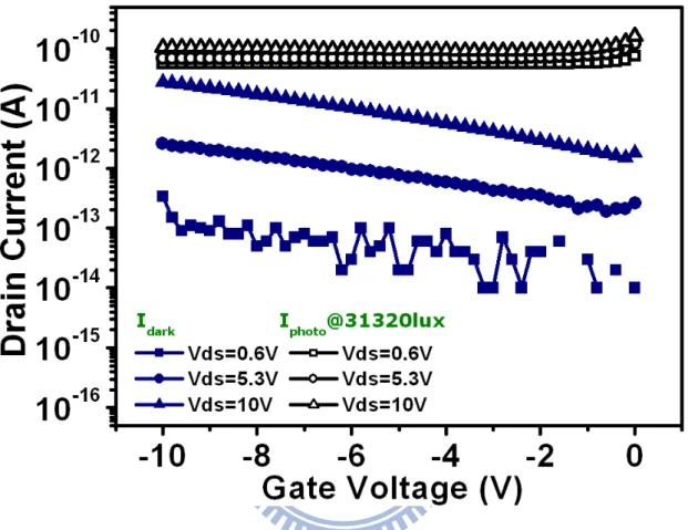
performance of light sensors. However, it may not be proper to be used to analyze photo leakage mechanism. As shown in Fig. 3-4, because ITotal is less dependent on the
gate voltage, RL/D is mostly determined by the behavior of IDark. It can not reflect
photo behaviors of TFTs. Therefore, for our discussion, it may be necessary to find another index which can eliminate the influence of IDark.
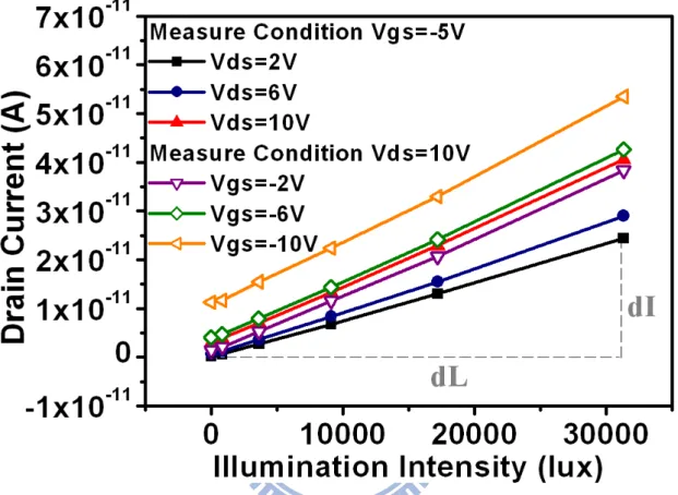
Fig. 3-5 shows the relationships between drain current and illumination intensity for several bias conditions in the off region. It can be seen that all drain currents are proportional to the amount of radiant illumination. Thus, it can be taken that the total leakage current under illumination (ITotal) is composed of two components: One is the
leakage current that is not caused by photo illumination (IDark) which is measured
under dark state. And the other part is illumination induced leakage current (IIllum)
which means the component induced by illumination. In this paper, we will offset IDark
and only consider IIllum which is defined to be the difference between ITotal and IDark.
To analyze the photosensitivity of the LTPS TFTs in detail, we further define the slope of the curve in which the current versus illumination intensity as Unit-Lux-Current (ULC in abbreviation) to be a new index. The physical meaning of ULC is the photo leakage current induced “per unit-photo flux” and independent of the dark current. Therewith, the total off current Itotal of LTPS TFT can be expressed as
L ⋅ + = + =I I I ULC
ITotal Dark Illum Dark (3-1) where L is the illumination intensity in lux.
22
3.3 Insight of Photosensitivity
3.3.1 Field Effects on Unit-Lux-Current
Fig. 3-6 shows gate bias dependence of ULC under different drain biases. It is obvious that ULC is change severely under higher drain voltage. Fig. 3-7 shows drain bias dependence of ULC under different gate biases. When drain voltage Vd is lower
than 8V, ULC increases linearly with drain bias [3.10], and gate bias effect is negligible. However, when Vd is large enough, ULC increases with drain bias more
rapidly and gate bias effect becomes significant. As shown by the arrow line in Fig. 3-7, the linear ULC curve at low drain bias can be fit, and this is one of the two components of the total ULC. This component which increases with drain bias linearly and independent of gate bias is defined as ULC1. Then, the second component
which subtracts ULC1 from the total ULC curve is called ULC2.
Furthermore, we plot ULC2 in Fig. 3-8. It is apparent that the log [ULC2] increases
with drain bias linearly, indicating that ULC2 increases with drain bias exponentially
when Vd is large enough. The parallel curves of log [ULC2] at different gate biases
indicate that the dependence of gate bias is also exponential. Thus, ULC can be expressed by a linear combination of these two components as
2 1 ULC ULC ULC = + (3-2) β α + = Vd ULC1 (3-3) Vg) -Vd ( exp ULC2 =γ ⋅ η1 η2 (3-4)
where α, β, γ, η1 and η2 are all fitting parameters. α and β correspond to the linear
drain voltage dependence and the zero drain bias offset of ULC1, respectively. γ is the
scaling factor of ULC2, while η1 and η2 are the parameters about the exponential
dependence on drain bias and negative gate bias of ULC2. As shown in Fig.3-9, the
calculated results agree with our experiment data very well. The values of fitting factors α, β, γ, η1 and η2 are listed in Table. 3-1.
23
Moreover, the mechanisms of two ULC components will be further discussed. The ULC can be taken into account both the leakage current induced in the gate-drain overlap depletion and in the lateral depletion regions [3.11]. When device is operating at the low drain voltage, the linear increase with drain bias of ULC1 is attributed to
lateral depletion region by the channel-drain junction in reverse bias. In this region, ULC2 is negligible. When drain voltage is large enough, ULC2 increase with drain
exponentially and gate bias effect becomes significant. Several mechanisms of leakage current were discussed in previous report [3.12-3.15]. It considered that the reverse lateral depletion at drain region extends and causes gate induced drain leakage (GIDL) in gate-drain overlap depletion junction. The amount of the photo current should be associated with the carrier generation in the space charge region. By the junction reverse saturation current and GIDL, the drain current owing to the GIDL effect is also in an exponential relation. This phenomenon is similar to our case of ULC2 component. The voltage difference between the drain and gate biases
corresponds to the magnitude of electric field across the depletion region. A more negative gate bias means that the electric field would get stronger, as the same as a more positive drain bias. It suggests that larger electric field across the drain depletion region causes larger photo effect. Both drain and gate bias affects the electric field strength in the depletion region in a slightly different ways.
3.3.2 Temperature Effects on Unit-Lux-Current
We further take into account the temperature effect of ULC. Fig. 3-10 shows the illumination effect on photo leakage current at different temperatures of 25, 40, and 60oC under a certain bias condition of (Vd ,Vg) = (10V, -5V). The correlation between
24
Drain bias dependences of ULC at different temperatures are shown in Fig. 3-11. ULC in the range of low drain bias is significantly affected by temperature. While in the higher drain bias range, the temperature effect reduces gradually. From the discussion above, we have separated the ULC intoULC1 and ULC2. It can be seen that
ULC1 is actually the term subject to the temperature effect. On the other hand, as
shown in Fig. 3-12, ULC2 is totally temperature independent, which means ULC2 is
the term purely induced by electric field. Therefore, ULC1 may be induced by
mechanism like excess carrier diffusion or thermionic emission and thus it has weak dependence on the electric field, especially gate bias. ULC2 may be induced by
mechanism like excess carrier drift or field emission and thus it has strong dependence on the drain and gate biases.
Since the lateral electric field is relatively small, the photo-induced current is a thermally generated current dominantly. The temperature effect on IDark can identify
constant activation energy [3.16-3.17], which hints us to add the fitting factors α and
β and in eq. (3-3) in the Arrhenius plot. Fig. 3-13 shows the relationship between α and β and 1/kT. These two factors increase with 1/kT exponentially and can be expressed by ) / (-exp Ea kT A⋅ A = α (3-5) ) / (-exp Ea kT B⋅ B = β (3-6)
where EaA, EaB are the activation energies of α and β, respectively, and A, B are their
corresponding fitting parameters. The fitting values of EaA, EaB, A and B are listed in
the inset. By the temperature effect discussed above, it is confirmative to separate ULC into two components. ULC1 is thermally activated and might be corresponding
to the thermionic emission or carrier diffusion, while ULC2 is independent of
25
3.3.3 Mechanism of Unit-Lux-Current
Based on the experimental results of bias, temperature, and sensing location, a more complete mechanism of ULC is proposed to explain photosensitive effect on the leakage current of LTPS TFT. Fig. 3-14 illustrates the band diagrams under the condition of Vg<0 along the channel direction near the drain region at low and high
drain biases. In the figure, Wd indicates the length of depletion region at the drain
electrode side where electron-hole pairs can be generated under illumination in the poly-Si film. The generated electrons flow toward the drain electrode and the holes flow in the opposite direction. Wd consists of two regions. One is the high hole
concentration region in the channel induced by the negative gate bias, the other is in the LDD region. The channel area is shielded by the gate metal, while the LDD region can be shined by the illumination. Based on the Poole-Frenkel effect lowering of a Coulombic barrier and phonon-assisted tunneling due to the electric field applied to a semiconductor [3.18], which enhances thermal emission and the trap-to-band field emission rate, the two components of ULC will be discuss. For the case at low drain bias with light irradiation, when the gate bias is changed, similarly to the abrupt p+n junction, the electric field of the other part in LDD region is invariable. Thus, the gate voltage independence of the ULC1 can be explained. As for the Vd effect, the lateral
depletion region increases linearly with drain bias, corresponding to the parameter α in eq. (3). With extremely low drain bias, there is still a depletion region in LDD, in accordance with the parameter β in eq. (3). The conduction mechanism of the leakage current in the low drain field is thermal emission [3.19]. Consequently, the parameters
α and of β of ULC1 are temperature dependent.
On the other hand, for the high drain bias with light irradiation, the electric field across the lateral depletion region is large enough to fully deplete the LDD region.
26
Therefore, the increase of drain voltage will increase the electric field within the limited LDD length pinched by the n+ region. In such case, the more negative gate bias will also result in the larger field with the same depletion width of the LDD region. The conduction mechanism of the leakage current at the high drain voltage is field enhanced emission in the space charge region [3.20]. The electric field dependence of ULC2 is reflected by the slightly different values of the fitting
parametersη1 and η2 in eq. (4).
3.3.4 Devices variation
The uniformity of LTPS TFT is always an important issue. Different devices even fabricated by the same process suffer from serious device variation, especially for the off current. For this consideration, the photo leakage currents would also vary among devices. Fig. 3-15 shows the photo leakage currents with respect to the illumination intensity of several devices on the same glass. It verifies that there is still serious device variation in the aspect of photo leakage current. The results further confirm that the mechanisms of the photosensitivity for the LTPS TFT are closely related to the different defect distribution or density in the grain boundary, alike the case of the dark off current. This issue needs to be overcome before LTPS TFTs can be practically used as the photo sensing device.
3.4 Conclusion
In this chapter, we present detail studies on the factors that affect the photo leakage current like bias condition, temperature, and defect states of the LTPS TFTs. It is found that photo leakage current always exhibits good linear dependence on
27
illumination intensity. Thus, a new index ULC characterizing the slope of the curve is introduced to discuss the photosensitivity. Furthermore, the mechanism of the photosensitivity for the LTPS TFTs is proposed. It relates to the width and electric field in the lateral depletion region near drain. It is also shown that ULC variation is also related to defects in the depletion region. The empirical equation of ULC provides a potential modeling for simulation of LTPS TFT circuitry considering the photo effect.
28
Figure 3-1 Photograph of the special U-shaped TFT with an arrow
indicating the scanning path of the illumination beam.
29
Figure 3-2 The drain current of the U-shaped TFT with the distance that
the illumination beam scanning along the channel direction.
30
Figure 3-3 The I
D-V
Gtransfer characteristics under illumination from
31
Figure 3-4 Gate bias dependence of LTPS TFT photo currents and dark
currents in off region.
32
Figure 3-5 The relationship between leakage current and illumination
intensity under different bias conditions.
33
34
35
Figure 3-8 The second component of Unit-Lux-Current (ULC
2) versus
36
Figure 3-9 The calculated and experimental data of drain bias effect on
Unit-Lux Current at different gate biases.
37
Fitting
Factors
Value
Unit
α
4.02x10
-17A/(V.Lux)
β
8.83x10
-16A/(Lux)
γ
1.61x10
-18A/(Lux)
η
10.42
1/V
η
20.14
1/V
38
39
Figure 3-11 Drain bias dependence of Unit-Lux-Current at different
temperatures.
40
Figure 3-12 The second component of Unit-Lux-Current (ULC2) versus
drain bias with different temperatures.
41
42
43
45
Chapter 4
Dependence of Photosensitive Effect on the Defects Created by DC
Stress for LTPS TFTs
4.1 Introduction
Low temperature polycrystalline silicon (LTPS) thin film transistors (TFTs) have attracted much attention for Active Matrix Liquid Crystal Display (AMLCD) and Active Matrix Organic Light Emitting Diode (AMOLED) applications due to the high mobility and the capability of realizing integrated circuits on the same glass [4.1]. For its application, several ambient light sensors using poly-Si TFTs, which is one of value-added functions for high-end flat panel display, have been reported [4.2-4.7]. The photosensitivity is a significant design consideration for achieving high image quality LCDs. However, it was reported that poly-Si TFTs suffer from several degradation mechanisms, such as hot carrier and self-heating effects [4.8]. Hot carrier effect, which was found that the degradation is related to the increase of strain bond tail states in the band gap of the poly-Si film, and damaged region, is near the drain. Self heating effect is reported interface states near the source region and the deep states in the poly-Si film near drain can be created [4.9]. It like as the SOI (Silicon on Insulator) devices, originated from the poor dissipation behavior of the substrate. As the operation voltage for VDS and VGS are high, the current conducting in the channel
is high and the joule heat, which can be rough calculated as P=IDS*VDS, would
become large and if the heat can’t be dissipated in time it will be accumulated in the active region, as shown in Fig. 4-1 [4.10]. As for the main application field for poly-Si
46
TFTs, the devices are fabricated on glass substrates and the heat transfer coefficients for the films in the device structure are shown in Fig. 4-2 [4.11]. As can be observed in the figure, if joule heat is generated in the poly-Si film during operation, the films surrounding poly-Si film with much smaller heat transfer coefficients than poly-Si film would in turn hinder the active region from dissipating heat. Due to such degradation, the photo-induced leakage current is strongly influenced which is difficultly designed for sensing circuits. In this work, we apply both stress conditions deliberately to manipulate the defect-related photo behaviors and modify Unit-Lux-Current (ULC) [4.12] equations in TFTs. Comparatively, this work focused on how additional non-uniform defects and the photo leakage mechanism influence both lateral and gate-drain overlap depletion.
In this study, the TFTs are measured under different illumination conditions before and after bias stress. One of the stress conditions is that the drain voltage is equal to 20V and the gate voltage is 3V, which is corresponding to the hot carrier effect. The other condition of self heating stress is set to be 15V for both the gate to source voltage Vgs and the drain to source voltage Vds.
4.2 Electrical Degradation of Poly-Si TFT under DC Stress
4.2.1 Photosensitivity Confirmation
In the previous study, it reveals the photo-induced current happens only at the drain side. To further confirm photo sensing area is mainly at the drain electrode side and photo-induced current is not affected mutually by source electrode, conventional lightly doped drain (LDD) structure and one side LDD structure of TFTs are designed for examination. Fig. 4-3 (a) and (b) show Ids-Vgs characteristics with negative gate
47
bias under different illumination conditions for conventional LDD device structure and only one-side LDD device structure. It can be seen that the off current of these two types of TFTs are lifted up to the similar levels under different illumination intensities. It also reveals poly-Si TFTs leakage current occurs at the depletion region of drain junction and not influenced from source region. Therefore, the following discussion of the photosensitivity mechanism will focus only on the drain region.
4.2.2 Model Description and Analysis
In this section, we take into account, the photo leakage current induced per unit-photo flux, Unit-Lux-Current (ULC in abbreviation) [4.10] to analyze the photosensitivity of the LTPS TFTs. ULC can be expressed by a linear combination of two components, both the leakage current induced in the lateral depletion and in the gate-drain overlap depletion regions [4.13]. When device is operating at the low drain voltage, ULC is attributed to lateral depletion region by the channel-drain junction in reverse bias. When drain voltage is large enough, ULC increase considered that the reverse lateral depletion at drain region extends as gate-drain overlap depletion junction. However, the photosensitivity of the LTPS TFTs is influenced from different both defect states distribution and density in the drain depletion region. Thus, in the aspect of poly-Si TFTs under electrical stress, additional defects created close drain depletion region, ULC is drastically varied after hot carrier and self-heating degradation, consequently.
As shown in Fig. 4-4 (a) (b), the Ids-Vgs transfer characteristics with 1V drain
voltage before and after hot carrier and self heating stress under different illumination conditions. In the previous study [4.14], it is revealed that photo-induced current tendency is changed oppositely by different stress conditions in lateral depletion
48
region by the channel-drain junction in reverse bias. It increases in the case of hot carrier, while it decreases for self heating. Meanwhile, it correlated the photosensitivity with device parameters such as mobility or threshold voltage, on the LTPS TFTs. Fig. 4-5 (a) show normalized ULC and mobility at Vds=0.6V and 10V in
accordance with stress time for hot carrier stress. The variation trends have been normalized, and then we can pay attention on the tendencies of these unit parameters. As figure shown, it reveals most trap states generated by hot carrier stress are crowded near drain junction side. In contrast, normalized ULC and threshold voltage at Vds=0.6V and 10V in accordance with stress time for self heating stress are
compared in Fig. 4-5 (b). It demonstrates that extra defect states created by self heating stress are spread in the whole poly-Si thin film through out the channel. From above mention, non-uniformly defect distributions after dc stress cause previous ULC equations not agree with experiment data very well. Therefore, the following discussion will focus on modifying ULC equations accurately for not only lateral but also gate-drain overlap depletion.
4.3 Insight of Defect-Related Photosensitivity
4.3.1 Empirical Defect-Related Unit-Lux-Current Model
Several mechanisms of leakage current were discussed in previous report [4.15-4.18]. For the purpose of effective medium modeling characteristics, we consider poly-Si to be a material with uniformly distributed trap density. Due to the photocurrent behaviors of LTPS TFTs concern with different types of additional non-uniform defects generated from various stress conditions, we suggest an empirical defect-related Unit-Lux-Current model to describe photosensitivity of the LTPS TFT after device degradation.
49
For analyzing trap-assisted leakage mechanism explicitly, an index Vdx used to further divide ULC into ULC1 and ULC2 to individually describe the influence of
lateral field and vertical field effects. At low drain bias, since the lateral electric field is relatively small, it considered that the photo-induced current is a thermally generated current dominantly. It hints us to adjust drain-bias dependence of Unit-Lux-Current model to approximately exponential forms. At higher drain bias, it considered that the reverse lateral depletion at drain region extends enhance vertical field effect and causes gate induced drain leakage (GIDL) in gate-drain overlap depletion junction. The amount of the photo current should be associated with the carrier generation in the space charge region. By the junction reverse saturation current and GIDL, the ULC2 owing to the GIDL effect is also in an exponential
relation. Base on conductivity limited by grain boundaries of semi-empirical analytical model. Thus, ULC can be modified by a linear combination of these two components as 2 1 ULC ULC ULC = + (4-1)
{
}
+χ ⋅ = exp[B (Vd-Vdx)]-1 ULC1 A1 1 (4-2){
exp[B (Vd-Vdx)]-1}
Vg) ( exp ULC2 = A2 ⋅ −η⋅ ⋅ 2 (4-3)where Vdx is an indication boundary drain voltage which demarcated the lateral
depletion and gate-drain overlap depletion region. (We can subtract ULC1 from the
total ULC curve. The rest part of the total ULC is the second component called ULC2.
The drain bias which makes Unit-Lux-Current from zero to positive point is an indication boundary.) χ is corresponding to photo leakage current induced by per unit-photo flux at Vdx (It is about 6.3V~6.46V before stress). A1, A2, B1, B2 and η are
all fitting parameters. A1 and A2 are corresponded to defect-related coefficients of
50
per unit depletion area. η is the scaling factor of ULC2 about the exponential
dependence on negative gate bias of ULC2.
4.3.2 Hot Carrier Effects on Unit-Lux-Current
The stress condition is that the drain voltage is equal to 12V and the gate voltage is 3V, which measured at different stress times of 1, 5, 25, 100, 500, 1000 sec to investigate the hot carrier effect on Unit-Lux-Current. The ULC at Vgs=-5V with
different stress times is shows in Fig. 4-6. Similarly, for analyzing photosensitivity on the defects influenced by lateral and vertical field effects, we also divide ULC measurement data into two components. It can be seen that the ULC increase and distort slightly at lower drain bias with stress times. However, when device operates at higher enough drain bias, the photo-induced current is severely decreased. The calculated and experimental data of drain bias effect on Unit-Lux-Current with different hot carrier stress times are individually shown in Fig. 4-7 (a) (b). It observed the calculated results agree with our experiment data very well. Fig. 4-8 (a) (b) shows the fitting factors A1, Α2 and Β, Β2 of modified ULC1 and ULC2 equations in eq. (4-2)
(4-3) at Vgs=-5V after hot carrier stress. It is noticed that drain voltage dependence per
unit depletion area, B1 and B2, are raised with stress times. The tendency of
defect-related coefficients, A1 and A2, of ULC1 and ULC2, are reduced with stress
times. It may attribute to the photo re-excited carriers increase and carriers transit slowly by trap hopping.
4.3.3 Self Heating Effects on Unit-Lux-Current
51
Vds, which measured at different stress times of 1, 5, 25, 100, 500, 1000 sec to
investigate the self heating effect on Unit-Lux-Current. The ULC at Vgs=-5V with
different stress times is shows in Fig. 4-9. By dividing ULC measurement data into two components, it is obvious that the ULC decrease under lower drain voltage and almost the same at higher drain bias with various stress time. In view of such condition, Fig. 4-10 (a) (b) show the calculated and experimental data of drain bias effect on Unit-Lux-Current with different self heating stress times. Similarly, Fig. 4-11 (a) (b) shows the fitting factors of modified ULC1 and ULC2 equations in eq. (3)
(4) at Vgs=-5V after self heating stress. It appears that, B1 and B2, A1 and A2, nearly
unchanged with various stress times. Even though hot carrier and self heating stress affect the device photosensitivity in a slightly different ways, verified ULC equations are still consisted with properly the illumination behaviors after self heating stress.
4.3.4 Mechanism of Unit-Lux-Current
The According to the experimental results of two stress conditions, a more complete mechanism of defect-related ULC is proposed to explain photosensitive effect on the leakage current of LTPS TFT after dc stress.
In previous chapter, for unstressed devices, it consists of LDD region and the high hole concentration region in the channel induced by the negative gate bias. The generated electrons move along drain electrode and the holes flow toward channel direction. For the case of devices at low drain bias with light irradiation, when the gate bias is changed, channel/LDD junction is similar to the abrupt p+n- junction. As the lateral depletion region increases with drain bias, the ULC1 of conduction
mechanism in the low drain field is thermal emission [4.19]. On the other hand, for the high drain bias with light irradiation, the gate-drain overlap depletion region