TiW(N) as Diffusion Barriers Between Cu and Si
Jung-Chao Chiou, Kuen-Chi Juang, and Mao-Chieh Chen*
Department of Electronics Engineering and the Institute of Electronics,
National Chiao-Tung University, Hsinchu, Taiwan
A B S T R A C T
TiW(N) and TiW are employed as diffusion barriers in the Cu/barrier/Si system. The thermal stability of Cu/TiW(N) a n d Cu/TiW contacted p*n junction diodes was investigated with respect to metallurgical reaction a n d electrical character- istics. The as-deposited TiW film formed body-centered cubic (bcc) structure, while the TiW(N) film formed face-centered cubic (fcc) structure. The Cu/TiW(600 ~)/Si structure remains intact up to 750~ 30 s rapid thermal anneal (RTA) in N2 ambient; at 775~ the Cu diffuses through the TiW layer to form Cu3Si with an overlayer of Ti-W-Si on the surface. The Cu/TiW(N)(600 A)/Si system is metallurgically stable up to 1000~ 30 s RTA in N2 ambient. The Cu/TiW(600 A)/p§ junction diodes were able to w i t h s t a n d the RTA annealing up to 675~ without losing the device integrity; however, the devices' characteristics are completely destroyed at temperatures above 775~ inconsistent with the occurrence of dramatic metal- lurgical reaction. The Cu/TiW(N)(600 A)/p*n junction diodes were able to withstand the RTA treatment up to 650~ without electrical characteristic degradation; a n d the devices' characteristics degrade gradually with the increase of RTA temper- ature.
Introduction
C o p p e r has b e e n considered as a potential metallization material in deep s u b m i c r o n integrated circuits because of its l o w resistivity (1.67 ~ - c m for bulk) a n d superior high electromigration resistance. ~-~ H o w e v e r , copper acts as a deep-level c o n t a m i n a n t in Si a n d reacts with Si to f o r m the c o m p o u n d Cu3Si at very l o w temperatures (200~ -n To use C u as an interconnection metal, an effective diffusion barrier layer is required to protect underlying devices f r o m C u contamination.
T h e r m a l stability of the Cu/diffusion-barrier/Si struc- ture has b e e n extensively studied lately to assess the poten- tial of various diffusion barriers, a n d m o s t of the results are s u m m a r i z e d in Ref. 12. A m o n g the various diffusion barrier materials, T i W [30:70 a t o m percent (a/o)] w a s f o u n d to be the m o s t effective one. 12 T i W barrier has also b e e n used in the A I / T i W / C o S i 2 a n d C u / T i W / C o S i 2 systems a n d has p r o v e d to be a useful diffusion barrier layer.13'14 In addition, it has b e e n reported that incorporation of nitrogen a n d o x y g e n in T i W film can i m p r o v e the barrier p e r f o r m a n c e in AI(Cu-Si)/W-Ti(N)/SiQ/Si a n d A u / T i W / A I / S i Q / S i sys- tems.1~-17 In this study, a T i W ( N ) layer, w h i c h w a s deposited by sputtering the Ti0.3W07 target in a m i x i n g gas of Ar:N2 = 1:5, w a s used as diffusion barrier in the C u / T i W ( N ) / p + n
diode structure a n d its barrier effect metallurgically a n d electrically investigated.
* Electrochemical Society Active Member. 2500 [] "~ 2000 E 1500 Z < lOOO ~d 500 J -- CuffiW/Si "---O'-- Cu/TiWN/Si
o o---o---o
0 ' ' 600 700 800 900 1000 1100 TEMPERATURE (*C)Fig. 1.o Sheet resistance
v s .annealing temperature for~ the
Cu(2000A)/TiW(600 A)/Si and Cu(2000 A)/TiW(N)(600 A}/Si
samples.
Fig. 2. SflM micrographs showing surface morphology for the (a)
Cu(2000 A)/TiW(600 A)/Si and (b) Cu(2000 A)/TiW(N)(600 A)/Si
samples after 900~ RTA in N2 for 30 s.
J. Electrochem. Soc.,
Vol. 142, No. 7, July 1995 9 The Electrochemical Society, Inc. 13_ ' / ) ' , / 3 U3 0 0 ' 0 0L5
:3 (.320
40
60
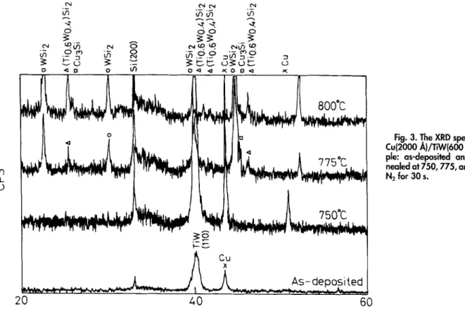
2327Fig. 3. The XRD spectra for the
Cu(2000 A)/TiW(600 A)/Si sam-
ple: as-deposited and RTA an-
nealed at 750, 775, and 800~ in
N2 for 30 s.
Experimental
Samples of Cu/TiW(N)/p+n and Cu/TiW/p*n diodes were fabricated for this study. The starting material was n-type, (100) oriented Si wafers with a nominal resistivity of 1 to
10 f~-cm. After initial cleaning, a 6000 /k field S i O 2 w a s thermally grown in a pyrogenic steam atmosphere at 1050~ Square contact regions w i t h area of 2.5 • 10 -3 cm 2 were defined by the photolithographic method. The sam- ples were cleaned again and then oxidized to grow 250 screen oxide for ion implantation. The p*n junctions were formed by BF~ i m p l a n t a t i o n at 70 keV to a dose of 5 • 1015 em -2 through the screen oxide, followed by annealing
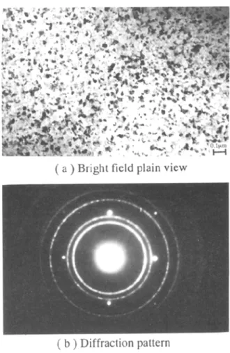
Fig. 4. EM micrographs of bright field plan view and diffraction
pattern for the as-deposited TiW film: (a) plan view and (b) diffraction
pattern.
Fig. 5. TEM
cross-sectionalmicrographs of the Cu(2000 A)/
TiW(600 A)/Si sample after RTA annealing in N~ for 30 s at (a) 750
and (b) 775~
2328
J. Electrochem. Soc.,
Vol. 142, No. 7, July 1995 9 The Electrochemical Society, Inc. 100 8O -E 6C 9 ~ ~c o 2c w 5(30 1000 1500 2000 2500 3000 Sputter Time (s]Fig. 6. Auger depth profile of the Cu(2000 A!/TiW(600 A)/Si sam-
ple after RTA annealing in N2 for 30 s at 775 C.
at a temperature of 900~ for 90 m i n in N2 ambient. A 600 ~- thick TiW(N) or TiW barrier layer was deposited. The TiW(N) film was deposited by sputtering using the TiW [Ti:W 10:90 weight percent (w/o)] target in a gas mixture of Ar:N2=I:5 a m b i e n t at a pressure of 5 • 10 -3 TorT and with a deposition rate of 1.7 A/s. The TiW layer was deposited using the same target and with the same conditions, except that pure Ar was used instead of an Ar/N2 mixture. The sampIes were exposed to air a n d then the Cu deposition followed. An 1800 A thick Cu film was deposited by sput- tering a Cu target (99.99%) in Ar a m b i e n t at a pressure of 5 x 10 -3 TorT; the deposition rate was 0.1 A/s. The samples were patterned into individual diodes by wet etching, using an etching solution for the Cu film of 5% H N Q , a n d a mixture of NH4OH + H202 + H20 = 1:1:1 for the TiW(N) a n d TiW films. The completed samples were treated with rapid thermal a n n e a l i n g (RTA) for 30 s at temperatures ranging from 300 to 1000~ Finally, A1 metallization was applied to the back side of each wafer for electrical measurement. U n p a t t e r n e d samples of Cu/TiW(N)/Si a n d Cu/TiW/Si structures were also fabricated following the same proce- dure for material analysis. Sheet resistance was measured by a four-point probe on the u n p a t t e r n e d samples. Surface morphology of the samples was inspected by scanning elec- tron microscope (SEM). S c a n n i n g Auger microscope (SAM)
Fig. 8. TEM micrographs of bright field plan view and diffraction
pattern for the as-deposited TiW(N) film: {a} plan view and (b) diffrac-
tion pattern.
w a s used for depth profile structure analysis. X - r a y dif- fraction ( X R D ) spectroscopy w a s used for material phase identification. Transmission electron microscope ( T E M ) w a s used to study the interacted layer structures a n d for crystal structure identification. Electrical characteristics
Fig. 7. The XRD spectra for the
Cu(2000 A)/TiW(N)(600 A)/Si
sample: as-deposited and RTA
annealed at 800, 950, and
1000~ in N2 for 30 s.
,j') CL (.9 0 >,, Z I(11~)
W2N Cu950"C
20
40
60
J. Electrochem. Soc.,
Vol. 142, No. 7, July 1995 9 The Electrochemical Society, Inc.
2329
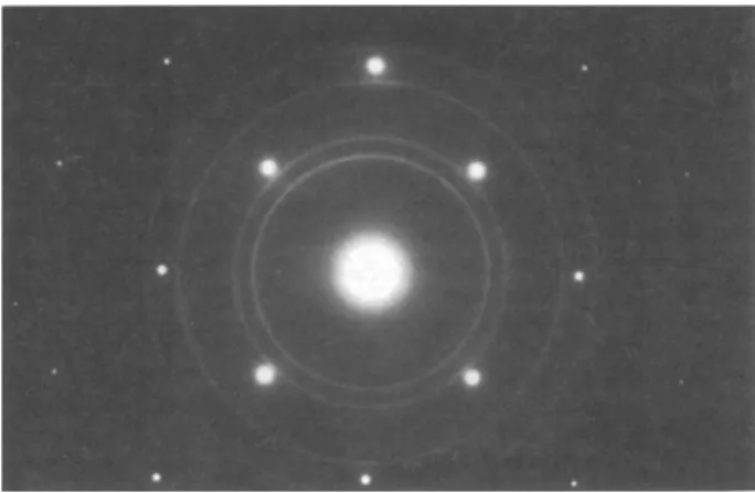
Fig. 9. TEM diffraction pattern for the TiW(N) film after RTA in N2 for 30 s at 1000~
of the diodes were measured with a semiconductor p a r a m - eter analyzer HP4145B.
Results and Discussion
Figure 1 s h o w s the sheet resistance Rs of the C u / T i W / S i a n d C u / T i W ( N ) / S i samples after 30 s R T A at various tem- peratures. A n abrupt Rs increase occurred o n the C u / T i W / Si s a m p l e after 775~ R T A ; s a m p l e surface color also c h a n g e d f r o m reddish yellow to silver-gray, suggesting that s o m e metallurgical reaction h a d occurred. O n the other hand, only a small Rs variation w a s observed o n the C u / T i W ( N ) / S i sample. In addition, the s a m p l e surface re- m a i n e d reddish yellow C u color even after reaching 1000~ R T A , although it b e c a m e slightly less glossy looking.
Surface m o r p h o l o g y of the C u / T i W / S i a n d C u / T i W ( N ) / S i s a m p l e s after E T A at 900~ is illustrated in Fig. 2. T h e C u / T i W / S i s a m p l e (Fig. 2a) looks silver-gray, appears to be m a d e u p of grains (identified as W - T i - S i as explained later in this section) about 30 p~m in size, a n d has a r o u g h surface morphology. Surface m o r p h o l o g y of the C u / T i W ( N ) / S i s a m p l e (Fig. 2b) s h o w s that it is c o m p o s e d of c o m p a c t C u grains about 1.5 ~ m in size.
T h e X R D results f r o m the C u / T i W / S i s a m p l e illustrated in Fig. 3 s h o w that C u a n d T i W reacted with Si to f o r m c o m p o u n d s of WSi2, (Ti0.~W0.~)Si2, a n d Cu~Si after 30 s R T A at 775~ T h e X R D (110) p e a k of the T i W film indicates that the lattice constant of the T i W film is 3.177 A. T E M tech- niques w e r e used to m a k e a m o r e detailed study of the T i W film. Figure 4 illustrates the bright field plan v i e w mi- e r o g r a p h a n d the diffraction pattern of the as-deposited T I W film, w h i c h is c o m p o s e d of intersected grains about i000 A in size. T h e diffraction pattern s h o w s that the crys- tal structure of the T I W film is body-centered cubic (bcc) with a lattice constant of 3.178 A, results consistent with the X R D analysis. T E M analysis of the 750~ annealed T i W film (not s h o w n ) revealed that the film's crystal a n d grain
A Fig. 10. Cross-sectional view TEM micrograph for the Cu(2000 )/TiW(N)(600 A)/Si sample after RTA annealing in N2 far 30 s at 1000~
structures were almost identical with those of the as-de- posited TiW film. The TEM cross-sectional micrographs of the Cu/TiW/Si sample shown in Fig. 5 reveal that the Cu/TiW/Si structure ~emained intact after RTA at 750~ (Fig. 5a). After RTA at 775~ the structure was completely destroyed by the formation of silicides; the TEM cross-sec- tional views show a Cu3Si precipitate surrounded by, SiO~ intruding into the Si substrate, ~s well as a c o m p o u n d layer covering the top surface. T h e A u g e r d e p t h profile of the C u / T i W / S i s a m p l e after R T A at 775~ s h o w n in Fig. 6, indi- cates that C u has diffused t o w a r d the Si substrate a n d f o r m e d Cu-silicide, while the surface layer is m a i n l y a c o m - p o u n d layer of Ti-W-Si. F r o m the X R D , A u g e r d e p t h pro- file, a n d T E M results, w e can conclude that a dramatic metallurgical reaction occurred within the C u / T i W / S i structure at a temperature of 775~ C o p p e r first diffused across the T i W layer a n d f o r m e d Cu3Si p h a s e at s o m e w e a k e r points; then, the T i W layer w a s transformed into the c o m p o u n d T i - W - S i o n the surface, w h i c h exhibited a r o u g h grain structure silver-gray in color as illustrated in Fig. 2a.
T h e X R D results f r o m the C u / T i W ( N ) / S i s a m p l e are illus- trated in Fig. 7. It w a s f o u n d that the as-deposited T i W ( N ) film contained a m i x t u r e of W 2 N a n d T i N phases. T h e cor- responding bright field T E M plan v i e w a n d diffraction
100[
r 675% 30s RTA
80I
Diode Area500 xS00//m 2
Number
of Diode= 40
6O
40 20 8O 700"C (b)50
20
_j
0
~ 750~
(c)
:E 80
(.9
o
< 6o
40
0
I 775=C
(d)
BO
6O
2O0
~0 0
i0-2
~0-4 10-~ S0-6 I0-S0
CURRENT DENSITY (Alcrn 2)
Fig. 11. Histogram of the reverse leakage current density for the Cu(2000 A)/TiW(600 A)/p*n diodes annealed with RTA at (a) 675, (b) 700, (c) 750, and (d) 775~ All leakage currents were measured at - 5 V bias.
2330
J. Electrochem. Soc., Vol. 142, No. 7, July 1995 9 The Electrochemical Society, Inc.
100
80
60
~0
2C0
80650'C 30s RTA
Diode
Area = 500x500/.tm 2
Number of Diode= 40
i I i i i i675"C
(b)
(a)l~0
8~
6o 2O0
I
775*c
(d)
80
60
4oLJl
2O0
100
10 -2
10- 4
10- 6
10
-8 10-10
CURRENT DENSITY (Alcrn
2)
Fig. 12. Histogram of the reverse leakage current density for the
Cu(2000 A)/TiW(N)(600 A)/p*n diodes annealed with RTA at (a)
650, (b) 675, (c) 700, and (d) 775~ All leakage currents were
measured at - 5 V bias.
p a t t e r n of the a s - d e p o s i t e d TIW(N) film in Fig. 8 show the a s - d e p o s i t e d TIWo(N ) film to be composed of compact grains about 100 A in size, and the diffraction p a t t e r n re- veals t h a t the a s - d e p o s i t e d film has a face-centered cubic (fcc) structure. Furthermore, the diffraction p a t t e r n seems to be composed of two closely spaced fcc diffraction rings. Both the W2N (ASTM Card:251257) and the TiN (ASTh/[ Card:381420) phases have fcc structures with lattice con- stants of 4.126 A (W2N) and 4.241 A (TIN), respectively, while the lattice constant estimated from the average r a - dius of the diffraction ring for the a s - d e p o s i t e d TiW(N) film is 4.208/k, which is close to the lattice constants of W2N and TIN. The XRD spectra in Fig. 7 also show t h a t the W2N phase remained stable, and no m e t a l l u r g i c a l reaction was observed on the Cu/TiW(N)/Si structure up to 1000~ In addition, the shift of the W2N (111) p e a k indicates t h a t the lattice constant decreased after RTA. The TEM p l a n view of the 1000~ RTA annealed TIW(N) film (not shown) revealed t h a t the a n n e a l e d film h a d a grain structure identical to t h a t of the a s - d e p o s i t e d film. The diffraction p a t t e r n of the 1000~ RTA annealed TiW(N) film as shown in Fig. 9 indi- cates t h a t the annealed film had a single-phase fcc struc- ture w i t h a lattice constant of 4.178 A, which is smaller t h a n t h a t of the a s - d e p o s i t e d TiW(N) film (4.208 ,~). F r o m the consistency of the XRD and TEM analysis results, we
can conclude t h a t the a s - d e p o s i t e d TiW(N) film consists of major W2N and minor TiN phases, and no obvious m e t a l - lurgical reaction occurred in the Cu/TiW(N)/Si structure up to 1000~ during RTA. Nevertheless, after the RTA an- nealing, the TiN phase vanished, and the lattice constant of TiW(N) decreased. Since the atomic r a d i u s of Ti (1.475/k) is close to t h a t of W (1.37/k) and is much smaller t h a n t h a t of N (2.83 /k), it is possible that, after high t e m p e r a t u r e an- nealing, Ti and N atoms in the TiN dissolved into the W2N structure forming the (TixW2_=)Ny compound and thus in- ducing the lattice constant shift.
Figure 10 shows the TEM cross-sectional m i c r o g r a p h of the 1000~ annealed Cu/TiW(N)/Si sample. The structure was basically preserved after 30 s RTA at 1000~ however, some voids were formed between Cu and the TiW(N) layers, and the Cu film h a d obviously undergone a reflow process which created a rough surface. The roughness and porosity of the Cu film supposedly resulted in a slight increase of Rs and a fuzzy looking sample surface.
Figure 11 shows the d i s t r i b u t i o n of reverse leakage cur- rent density Jr measured at - 5 V on 40 r a n d o m l y chosen Cu/TiW/p+n junction diodes. The diode characteristics de- g r a d e d after RTA at 700~ and further deteriorated with further increases in annealing temperature. After 775~ annealing, all junctions were severely d a m a g e d (Fig. l l d ) , which is consistent w i t h the d r a m a t i c metallurgical reac- tion t h a t occurred at this temperature. S i m i l a r Jr measure- ments were m a d e on the Cu/TiW(N)/p+n junction diodes, and the results are i l l u s t r a t e d in Fig. 12. Although the Cu/ TiW(N)/Si structure is more metallurgically stable t h a n the Cu/TiW/Si structure, the Cu/TiW(N)/p§ diodes started to degrade at a slightly lower annealing t e m p e r a t u r e of 675~ and the junction d e g r a d e d g r a d u a l l y as annealing t e m p e r a - ture was increased. Figure 13 shows the average leakage current density vs. armealing t e m p e r a t u r e for the Cu/TiW/ p+n and Cu/TiW(N)/p§ junction diodes. The Cu/TiW(N)/ p+n diodes a p p a r e n t l y become more stable electrically t h a n the Cu/TiW/p+n diodes when the annealing t e m p e r a t u r e exceeds 775~ D e g r a d a t i o n of the C u / b a r r i e r / S i junction structure, electrical characteristics always occurs before the metallurgical reaction. Since Cu is a fast diffusion spe- cies in Si, d e g r a d a t i o n of the junction will d e p e n d on w h e t h e r the b a r r i e r layer can or cannot prevent the Cu from p e n e t r a t i n g through the b a r r i e r layer. Although the Cu/TIW(N)/Si system is more metallurgically stable t h a n the Cu/TIW/Si system, and we did hope t h a t the incorpo- r a t e d nitrogen would be segregated at the g r a i n boundaries to r e t a r d the diffusion p a t h s for Ca atoms, the diffusion- b a r r i e r effect of TiW(N) a p p a r e n t l y did not prevent Cu p e n - etration. It is possible t h a t the smaller grains in the TiW(N) layer offer more p a t h alternatives for Cu diffusion.
1 0 -1. 1 0 -2. 10.~"
10"4"
10.5 .
10"6"
107" 10-8 10 -9 600 700 800 TEMPERATURE (~ @ CuffiW/Si - - - O - - - Cu/TiW(N)/Si 900Fig. 13. Average reverse leakage current density measured at
- 5 V for the RTA annealed Cu(2000 A)/TiWI600 A)/p*n and
Cu(2000 A)/T,~'(N)(600 A)/p§ iunction diode.
J. Electrochem. Soc.,
Vol. 142, No. 7, July 1995 9 The Electrochemical Society, Inc. 2331Conclusion
Thermal s t a b i l i t y of Cu/TiW(600 A)/p~n and Cu/TiW(N) (600 A)/p§ diodes were investigated w i t h respect to the diffusion-barrier effects of TiW and TiW(N) b a r r i e r layers for Cu metallization. The TiW film has a W bcc structure, while the TiW(N) film has a W2N fcc structure. The Cu/ TiW/Si system is metallurgically stable up to 30 s RTA an- nealing at 750~ while the Cu/TiW(N)/Si structure re- mains b a s i c a l l y stable up to 1000~ The Cu/TiW/Si structure was destroyed after RTA annealing at 775~ with the formation of a Cu3Si phase that intruded into the Si substrate, a n d the formation of a W-Ti-Si c o m p o u n d layer covering the s a m p l e surface. T h e electrical characteristics of the C u / T i W / p + n junction diodes started to degrade at 7O0~ a n d the diodes' reverse current m a d e a drastic in- crease at 775~ O n the other hand, the C u / T i W ( N ) / p § junction diodes started to degrade at 675~ a n d the reverse current increased gradually with increasing annealing temperature. A s a result, the Jr of the C u / T i W ( N ) / p + n diodes is smaller than that of the C u / T i W / p + n diodes after R T A annealing at temperatures a b o v e 775~
Acknowledgment
The authors wish to t h a n k the S e m i c o n d u c t o r Research Center of N a t i o n a l Chiao-Tung University and the Na- t i o n a l Nano Device L a b o r a t o r y for providing excellent processing environment. This w o r k was s u p p o r t e d by the N a t i o n a l Science Council, ROC, under Contract No. NSC- 82-0404-E009-400.
M a n u s c r i p t s u b m i t t e d Sept. 12, 1994; revised m a n u s c r i p t received Jan. 17, 1995.
National Chiao-Tung University assisted in meeting the publication costs of this article.
R E F E R E N C E S
i. H . K . K a n g , J. S. H. Cho, a n d S. S. W a n g ,
I E E E Electron
Device Lett.,
E D L - 1 3 , 448 (1992).2. C. W. P a r k a n d R. W. Vook,
Appl. Phys.
Lett., 59, 175 (1991).3. J. Tao, N. W. C h e u n g , C. H u , H. K. K a n g , a n d S. S. Wang, IEEE Electron Device Lett., EDL-13, 433
(1992).
4. P. L. Pat, C. H. Ting, C. Chiang, C. S. Wet, a n d D. B. Fraser, Mater. Res. Soc. Symp. Proc. VLSI V, p. 359
(1990).
5. T.E. Seidel, Mater. Res. Soc. Symp. Proc., 260, 3 (1992).
6. A. Cros, M. O. Aboelfotoh, and K. N. Tu, J. Appl. Phys.,
67, 3328 (1990).
7. S . H . Corn, J. L. Falconer, and A. W. Czanderna, J. Vac. Sci. Technol., A6, 1012 (1988).
8. S. Q. Hong, C. M. Comrie, S. W. Russell, and J. W. Mayer, J. AppI. Phys., 70, 3655 (1992).
9. R. Padiyath, J. Seth, S. V. Babu, and L. J. Matienzo,
ibid., 73, 2326 (1993).
10. L. Stolt, E M. D'Huerle, a n d J . M. E. Harper, Thin Solid Films, 200, 147 (1991).
11. S. D. Brotherton, 5. R. Ayres, A. Gill, H.W. van Kesteren, and E J. A. M. Greidanus, J. Appl. Phys.,
62, 1826 (1987).
12. S. Q. Wang, S. Suthar, C. Hoeflich, and B. J. Burrow,
ibid., 73, 2301 (1993).
13. E M. Yang a n d M. C. Chen, J. Vac. Sci. Technol., B l l ,
744 (1993).
14. J. C. Chiou and M. C. Chen, This Journal, 141, 2804
(1994).
15. J.M. Oparowski, R. D. Sisson, Jr., and R. R. Biederman,
Thin Solid Films, 153, 313 (1987).
16. A. G. Dirks, R. A. M. Wolters, and A. J. M. Nellissen,
ibid., 1931194, 201 (1990).
17. R. S. Nowicki, J. M. Harris, M. A. Nicolet, and I. V. Mitchell, ibid., 53, 195 (1978).