This content has been downloaded from IOPscience. Please scroll down to see the full text.
Download details:
IP Address: 140.113.38.11
This content was downloaded on 25/12/2014 at 02:41
Please note that terms and conditions apply.
Multilayer rapid-drying blade coating for organic solar cells by low boiling point solvents
View the table of contents for this issue, or go to the journal homepage for more 2014 Jpn. J. Appl. Phys. 53 062301
(http://iopscience.iop.org/1347-4065/53/6/062301)
Multilayer rapid-drying blade coating for organic solar cells by low boiling point solvents
En-Chen Chen1, Pei-Ting Tsai2, Bo-Jie Chang1, Chun-Ming Wang2, Hsin-Fei Meng2*, Jia-Ying Tsai3,
Yu-Fan Chang4, Zhi-Kuan Chen5, Chang-Hung Li4, Yung-Hsuan Hsu2, Chun-Yu Chen2,
Hao-Wu Lin6, Hsiao-Wen Zan4, and Sheng-Fu Horng1
1Department of Electrical Engineering, National Tsing Hua University, Hsinchu 300, Taiwan 2Institute of Physics, National Chiao Tung University, Hsinchu 300, Taiwan
3Institute of Photonics Technologies, National Tsing Hua University, Hsinchu 300, Taiwan
4Department of Photonics and the Institute of Electro-Optical Engineering, National Chiao Tung University, Hsinchu 300, Taiwan 5Institute of Materials Research and Engineering, 3 Research Link, Singapore 117602
6Department of Materials Science and Engineering, National Tsing Hua University, Hsinchu 300, Taiwan
E-mail: [email protected]
Received January 20, 2014; accepted February 20, 2014; published online May 9, 2014
A bulk heterojunction organic solar cell with poly(3-hexylthiophene) (P3HT) as the donor and (6,6)-phenyl-C61-butyric acid methyl ester (PCBM) as the acceptor is deposited using blade coating on a hot plate at 80 °C with hot air of 70 °C applied from above. In contrast to the 30 min of conventional dichlorobenzene solvent annealing, the rapid-drying blade coating forms a dryfilm in 1 s. The fabrication throughput is substantially enhanced. The blade-coatedfilm has a smoother surface roughness of 3.5 nm compared with 10.5 nm for solvent annealing; however, the desired phase separation in the 50 nm scale forms despite the rapid drying. A single layer solar cell exhibits power conversion efficiency of 4.1% with blade coating in chlorobenzene, which is the same as solvent annealing device. A multilayer device with carrier blocking layers fabricated entirely of the less toxic toluene also exhibits efficiency of 4.1%. ©2014 The Japan Society of Applied Physics
1. Introduction
An efficient organic solar cell can be produce when an elec-tron donor is blended with an acceptor to form a bulk hetero-junction, in which the donor and acceptor are phase separated in the 10 nm scale and form individual connected pathways for the collection of electrons and holes under optical excitation. In most cases, the donor is a conjugated polymer, whereas the acceptor is a fullerene derivative. Most of studies on polymer solar cells have used only a single active layer. A multilayer device structure can enhance the efficiency of an organic light-emitting diode (OLED) by introducing the carrier blocking layers. These blocking layers are crucial to organic solar cells because they prevent the electrons from entering the anode and prevent holes from entering the cathode. However, most solution coating methods for organic solar cells do not allow multilayer deposition because of dissolution. The blade coating methods enables multilayer solution deposition for OLEDs.1–3) It is also applied to organic solar cells4)with only a single active layer. A small molecule solar cell can be readily produced in multilayers using vacuum evaporation;5) however, the lack of a proper bulk-heterojunction decreases the efficiency. Vertical phase separation of the electron donor and acceptor in polymer solar cells can be achieved by controlling the fabrication process;6,7)however, only a graded structure can be realized and the effect of a true sharp blocking layer remains unknown.
A modified rapid-drying blade coating method is applied to fabricate a multilayer polymer solar cell with electron and hole blocking layers. Dissolution was avoided because of the rapid solvent evaporation caused by the effect of simulta-neous substrate heating from the bottom and hot wind from above.8) The wet film deposited by the blade motion was dried immediately before dissolution of the power solid layer. This method has only been applied to single-layer polymer solar cells in normal8)and inverted9)structures. In addition to carrier blocking by the multilayer structure, rapid-drying blade coating has the advantage of high process throughput
compared with the conventional solvent annealing with slow drying in a high boiling-point solvent (such as dichloroben-zene), followed by post thermal annealing.10) Although post annealing can be removed by additives during spin coating11) and roller painting,12) slow drying is necessary for high efficiency. When brush painting on a hot plate is reported,13) the uniformity is a concern and the efficiency is moderate.
Using chlorobenzene as the solvent, single-layer rapid-drying blade coating produces power efficiency of 4.1%, which is close to the value obtained using conventional slow-drying solvent annealing in dichlorobenzene. This indicates that optimized donor–acceptor phase separation can be achieved rapidly with high process throughput. This result indicated that a slow drying process is unnecessary for the donor and acceptor molecules to move around and form the phase-separated domains of tens of nanometers, which leads to high efficiency. A multilayer structure for chlorobenzene blade coating produces the same efficiency, suggesting that the blocking layers are unnecessary after optimizing the active layer morphology. Conversely, blade coating in toluene does not optimize active layer phase separation. Therefore, a multilayer structure increased the efficiency from 2.5% for a single layer to 4.1% for a trilayer in toluene. Rapid-drying blade coating combines the advantages of multilayer, high production throughput, low solvent toxicity, phase separation, and high efficiency. In addition, almost no material waste occurs during the blade coating process. 2. Experimental procedure
Polymer solar cells have a structure of pre-patterned indium– tin-oxide (ITO) glass/PEDOT:PSS/P3HT:PCBM/Ca/Al. PEDOT:PSS is poly(3,4-ethylenedioxythiophene):poly(sty-rene sulfonate) (CLEVIOS™ PVP AI4083, purchased from HC Starck). A bulk heterojunction organic solar cell with poly(3-hexylthiophene) (P3HT) as the donor and (6,6)-phenyl-C61-butyric acid methyl ester (PCBM) as the accep-tor is deposited using blade coating method. The ITO coated glass substrates were cleaned in an ultrasonic bath for 20 min using acetone and were subsequently rinsed three times using
http://dx.doi.org/10.7567/JJAP.53.062301
deionized water and cleaned using UV ozone cleaner for 20 min. The 40 nm PEDOT:PSS layer was spin coated at 2000 rpm on a pre-cleaned ITO substrate and baked at 200 °C in nitrogen for 15 min. For the active semiconductor layer, a1 : 1 weight ratio of the P3HT:PCBM blend was used. The solution concentration of the active layer was 1.7 wt % in dichlorobenzene for spin coating and 1.7 wt % in chloroben-zene for blade coating, respectively. After coating, all P3HT:PCBM layers were annealed at 140 °C for 20 min in nitrogen. To examine the multilayer structure devices, a 15 nm pure P3HT electron blocking layer and a 10 nm pure PCBM hole-blocking layer were added using blade coating. The rapid-drying blade coating was performed on a hot plate at 80 °C. The blade had a gap of 60 µm. The solution (30 µL) was delivered in front of the blade using a pipette, and the blade was subsequently moved by hand at approximately 40 cm s¹1to cover the 4 mm2active area of the device with wet film. Hot air from a hair dryer was applied to enhance the drying and uniformity. Dryfilms formed in approximately 1 s for chlorobenzene and 0.7 s for toluene. The air temper-ature was approximatly around 70 °C after passing the hair dryer to the wind mask, as shown in Ref.8. The distance between the wind mask and thefilm was maintained at 1 cm. A tolerance window for air temperature exists because it must be sufficiently high to ensure drying within a few seconds; however, it must not be excessively high to cause morphological changes though annealing.
In spin-coating cases, the thickness of the active layer was 250 nm at a spin rate of 600 rpm for 40 s; the wetfilm was subsequently dried slowly for 30 min during solvent anneal-ing. A Ca (35 nm)/Al (100 nm) electrode formed on top of the active layer because the thermal evaporation was below 10¹6Torr. All devices were packaged in a glove box and measured in the ambient environment. For characteristics of solar cell devices, the power conversion efficiency (PCE) was measured using a solar simulator (San-Ei XES-301S) under AM1.5 G of irradiation. The incident photon-to-conversion efficiency (IPCE) is defined as the average number of photo-generated charge carriers contributing to the current per incident photon. It was measured using a lock-in amplifier under a short-circuit condition when the devices were illuminated by monochromatic light from a 250 W quartz– tungsten–halogen lamp (Osram) passing through a mono-chromator (Spectral Products CM110). Calibration of the incident light was performed using a monocrystalline silicon diode. To avoid the overtone effect of the monochromator, we used a high-pass filter to remove the wavelengths lower than 560 nm. For analyses of various deposition-method films, the surface morphology and phase were monitored using an atomic force microscope (AFM; Digital Instruments Dimension 3100). The absorption spectrum was measured using a UV–visible spectrophotometer (HP8453). The photo-luminescence spectrum was measured by fluorescence spec-trometers (Hitachi F-4500). The nanostructure was examined using X-ray diffraction (XRD; D1 System BEDE).
3. Results and discussion
The solar cell characteristics of single layer devices with various deposition methods are shown in Fig. 1(a). The blendfilm thickness was fixed at 250 nm. Blade coating with rapid drying in chlorobenzene with a boiling point of 131 °C
produced power conversion efficiency of 4.11%, similar to the efficiency of 4.14% of solvent annealing in dichloro-benzene with a high boiling point of 180 °C. Spin coating in chlorobenzene produced only 3.01% efficiency, proving that blade coating is crucial to high efficiency with the same solvent.
The topography and phase images of AFM of thefilms are shown in Fig. 1(b). Solvent annealing produced high rough-ness of 10.5 nm,10) whereas blade coating resulted in much lower roughness of 3.5 nm. Spin coating resulted in the lowest roughness of 0.95 nm because the film dried during spinning. The phase images show the domains of P3HT and PCBM in a smaller scale than the topography image. Blade coating and solvent annealing separated the P3HT and PCBM domains by approximately 50 nm, whereas spin coating in chlorobenzene resulted in a more uniform mixing of the two components with small scattered domains. The domains of the film produces by toluene blade coating are smaller, indicating that toluene does not result in sufficient phase separation. The phase images are directly correlated to the device performance because large domains are required for
-15 -10 -5 0 5 10 15
Current Density (mA/cm
2) Voltage (V) DCB spin CB blade CB spin Tol blade Jsc(mA/cm2 ) 0.0 0.1 0.2 0.3 0.4 0.5 0.6 0.7 Voc(V) FF PCE(%) 10.91 0.60 0.63 4.14 10.25 0.60 0.66 4.11 8.79 0.59 0.57 3.01 6.66 0.61 0.60 2.50 (a) (b)
Fig. 1. (Color online) (a) Solar cell current density vs voltage (J–V) characteristics of spin coated P3HT:PCBM in dichlorobenzene (DCB) solution, blade coated P3HT:PCBM in chlorobenzene (CB) solution, spin coated P3HT:PCBM in chlorobenzene solution and blade coated
P3HT:PCBM in toluene (Tol) solution. (b) AFM topography (left) and phase (right) images of single layer devices with various deposition methods.
Jpn. J. Appl. Phys. 53, 062301 (2014) E.-C. Chen et al.
high efficiency. The substantial difference between the surface roughness for solvent annealing and blade coating does not affect the device efficiency. The large grains around one micron in solvent annealing are unnecessary for high efficiency. Note that the term “domain” is used to describe the phase separation of the P3HT donor and PCBM acceptor measured by the phase images of AFM in Fig. 1(b). Since the phase angle in AFM can differentiate the type of materials, we assume the domain in the phase image correspond to either donor or acceptor. In the bulk heterojunction solar cell high performance is reached when the donor and acceptor are inter-penetrating with the size close to exciton diffusion length, which is the case of chlorobenzene blade coating and dichlorobenzene solvent annealing. On the other hand, the term “grain” is used to describe the large surface height variation in the dichlorobenzene solvent annealing, which has about 10 nm in height and 10 µm in area. Such grain is only a feature of surface topography and may contain a mixing of donor and acceptor. The domain in phase image and grain in topography are therefore independent morphology structures. In the device data below the large grain about 10 micron is absent in the chlorobenzene blade coating solar cell and is not necessary for high efficiency. Contrarily, the domain size is closely related to the solar cell performance.
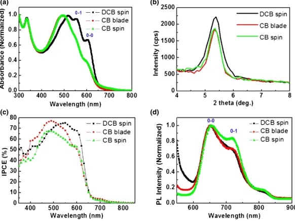
The deposition method of the P3HT:PCBM blendfilm has a considerable effect on the crystallinity of the P3HT domain. The absorption spectrum, photoluminescence spectrum, and XRD were used to examine the P3HT structure. The optical absorption included a 0–0 transition and 0–1 transition, corre-sponding to the absorption of a photons, with the creation of 0 and 1 phonons respectively. For an isolated chain, the 0–0
transition was dipole-allowed and had high oscillator strength for P3HT. When the chains aggregate, the single-chain exciton states are coupled to form an exciton band and the oscillator strength is reduced.14,15) When a high intra-chain order occurs, the exciton state is de-localized and the inter-chain coupling is weak; therefore, so the 0–0 transition remains relatively strong.15)Figure 2(a) shows the absorption spectra of the blend using various deposition methods. Films produced by dichlorobenzene solvent annealing exhibited the highest 0–0 transition, implying that it has a high order in the P3HT domain compared to blade coated and chlorobenzene spin-coated films. Figure 2(b) shows a higher (100) peak in XRD for the dichlorobenzene film compared with the other methods is consistent with the absorption spectrum. Indeed the (100) peak is corresponded to the spacing between the alkyl chains16)and is closely related to the main-chain order exhibited in the absorption spectrum. The absorption spec-trum correlated with the incident photon-to-conversion efficiency spectrum, as shown in Fig. 2(c). The PL spectrum exhibited phonon bands including the 0–0 transition and 0–1 transition where 0 and 1 phonons were created together with the emitted photon. In the aggregate states for P3HT chains, the 0–0 luminescence transition that occurred from the lowest level of the exciton band was caused by coupling and was dipole-forbidden. Therefore, the relative strength of the 0–0 transition was a measure of disorder. Figure 2(d) shows the PL spectrum of thefilms using various deposition methods. Chlorobenzene spin coating resulted in the lowest relative 0–0 transition and the highest inter-chain order along the ³-stacking direction. Blade coating and solvent annealing resulted in lower inter-chain order for P3HT. Therefore, blade coating yields the lowest level of the P3HT domain order,
(a) (b)
(c) (d)
Fig. 2. (Color online) (a) Absorption spectrum, (b) XRD, (c) IPCE spectrum, and (d) PL spectrum of the single blend layer devices with various deposition methods.
regardless of whether it is intra-chain or inter-chain. This occurred because it has the shortest drying time among all three deposition methods and P3HT chains have the lowest chance to align into highly crystalline structures. The results of AFM images and optical spectroscopy showed that the phase separated domain formation is more crucial than the polymer chain order inside the domains for device perform-ance. In the conventional slow solvent annealing process, P3HT/PCBM phase separation and the P3HT chain packing occur simultaneously. In this case, it is difficult to separate the effects of phase separation and packing order on the solar cell performance. Using rapid-drying blade coating, P3HT was less ordered, but phase separation occurred nonetheless. Packing and phase separation occurs at various time scales and lacks sufficient time for packing; however, the time is sufficient for 20–50 nm phase separation.
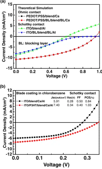
Multilayers of organic semiconductor films can be deposited by blade coating without dissolution because of the rapid drying. This method has been successfully applied in organic light-emitting diodes by adding carrier blocking layers.1–3) Therefore, studies have focused on determining whether the solar cell efficiency can be increased by adding carrier blocking layers using blade coating. In the bulk heterojunction layer, an electron and hole are generated when a photon is absorbed. Under the built-in field, the electron moves to the low work function cathode of Ca and the hole moves to the high work function anode of PEDOT:PSS. However, a fraction of electrons may diffuse into the anode and the holes into the cathode, and such diffusion current partially cancels the photo-current and reduces the efficiency. The electron blocking layer of pure P3HT next to the anode and the hole blocking layer of pure PCBM next to Ca remove unwanted diffusion current. The dark carriers near the Ohmic contacts caused by local thermal equilibrium prevent the diffusion current from entering the electrodes. For example, the electrons encounter a high hole density near the PEDOT:PSS interface and mostly recombine before entering the anode.17,18) The dark carriers are absent only when a sufficiently high barrier is present between the electrode and the semiconductor bands; that is a Schottky contact. A theoretical simulation for Ohmic and Schottky contacts is shown in Fig. 3(a). For the theoretical simulation, physical parameters from the system of the P3HT donor and PCBM acceptor blend were selected; the electron affinity of PCBM was 3.7 eV and the ionization potential of P3HT was 5.1 eV. The thickness of the blend layer was 200 nm. For a Schottky contact, the barrier height of the carrier injection was 0.4 eV and was symmetrical. The blocking layer thickness was 10 nm for the thickness. The hole and electron mobility are 3© 10¹4 and 2.5© 10¹3cm2V¹1s¹1in this simulation, respectively. The blocking layer does not affect the Ohmic contact and increases the open circuit voltage (Voc) for a Schottky contact. The program was described in a previous study.18) A number of studies have indicated that blocking layers enhance efficiency7,19) because the blend layer does not have a balanced electron and hole mobility. This type of imbalance may cause carriers to may accumulate in the blend and diffuse into the opposite electrode, even in Ohmic contacts. Using blade coating in chlorobenzene, 15 nm of pure P3HT and 10 nm of pure PCBM were added in three configurations: P3HT/blend (p–i), blend/PCBM (i–n), and
P3HT/blend/PCBM (p–i–n). Within a statistical variation of approximately 10%, no difference was observed in the efficiency for these configurations and the single layer device with a mean value of approximately 4%. This implies that, after the carrier mobility in the blend is optimized, the multi-layer structure cannot further enhance the performance, which is consistent with the simulation in Fig. 3(a). Con-versely, the Schottky contact forms when the PEDOT:PSS layer is intentionally removed because ITO has a 0.4 eV hole barrier to the P3HT valence band. As expected from the simulation on the Schottky barrier, the efficiency shown in Fig. 3(b) increased considerably from 0.84 to 1.03% when the electron blocking layer was added. In addition to the increase ofVoc, as predicted theoretically, the increase ofJsc may be attributed to the additional absorption in the pure P3HT layer, which was not included in the simulation. The problem in the Schottky barrier device is the lowVoccaused by the small work function difference relative to the Ohmic contact devices.
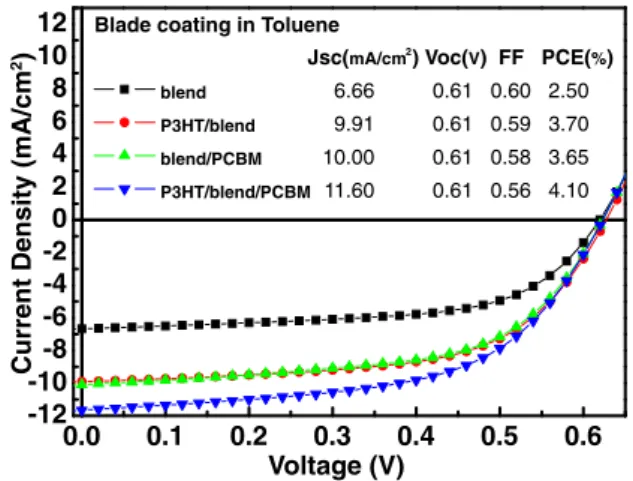
In contrast to chlorobenzene blade coating, a multilayer structure has a considerable effect on the device performance for toluene blade coating, as shown in Fig. 4. Single-layer toluene blade coating with rapid drying produces efficiency of 2.5%. This is attributed to the weak solubility of toluene,
-15 -10 -5 0 5 10 15
Current Density (mA/cm
2) Voltage (V) Theoretical Simulation Ohmic contact PEDOT:PSS/blend/Ca PEDOT:PSS/BL/blend/BL/Ca Schottky contact ITO/blend/Al ITO/BL/blend/BL/Al BL: blocking layer 0.0 0.2 0.4 0.6 0.8 1.0 (a)
0.0
0.1
0.2
0.3
-12 -10 -8 -6 -4 -2 0 2 4 6 8 10 12Jsc(mA/cm2) Voc(V) FF PCE(%)
5.91 0.28 0.50 0.84 7.40 0.34 0.40 1.03
Current Density (mA/cm
2)
Voltage (V)
Blade coating in chlorobenzene Schottky contact ITO/blend/Ca/Al
ITO/P3HT/blend/Ca/Al (b)
Fig. 3. (Color online) (a) Theoretical simulation of blocking layer (BL) effect in Ohmic and Schottky contacts. (b) Solar cellJ–V characteristics of Schottky contact devices with blocking layer by blade coating in chlorobenzene solution.
Jpn. J. Appl. Phys. 53, 062301 (2014) E.-C. Chen et al.
resulting in inferior bulk heterojunction morphology with small domains, as shown in Fig. 1(b), and low hole mobility. A single-layer device produced using toluene blade coating has efficiency of over 3% for the thick active layer;4) however, it is highly sensitive to process details and has inferior reproducibility, which may be attributed to the lower solubility in toluene. The AFM image of the toluene device is shown in Fig. 1(b); the small domain in the phase image for P3HT and PCBM indicates insufficient phase separation in the active layer through blade coating in toluene, and the bulk heterojunction morphology is not in the optimized state compared with the case of chlorobenzene blade coating. When a pure P3HT electron blocking layer of 15 nm and a pure PCBM hole blocking layer of 10 nm was added, the efficiency increased to 3.7 and 3.65%, respectively. When both blocking layers were added, the efficiency increased to 4.1%, the same as the single-layer chlorobenzene and solvent annealing devices. The non-optimized donor–acceptor mor-phology in the toluene device was optimized in the multilayer structure.
4. Conclusions
A multilayer polymer solar cell with carrier blocking layers was produced using rapid-drying blade coating with simultaneous heating from the substrate hot air from above to avoid dissolution. The donor–acceptor phase separation and morphology are sensitive to the coating method and the solvent. A multilayer structure is not required after the active layer optimizes phase separation, which is achieved using conventional dichlorobenzene spin coating or chlorobenzene
blade coating. Conversely, if the active layer does not optimize phase separation, as in the case of toluene blade coating, a multilayer structure is crucial to increase the effi-ciency to the same level as that of the optimized active layer. In a multilayer structure deposited using toluene, which is less toxic and has a low boiling point power conversion efficiency of 4.1% can be obtained, which is the same as the solvent annealing device. Using rapid-drying blade coating with toluene, an efficient organic solar cell can be fabricated with high throughput in an environmentally friendly manner.
Acknowledgments
This work was supported by the National Science Council of Taiwan under grant Nos. 99-2628-M-009-001, 98-2112-M-007-028-MY3 and the Ministry of Economic Affairs of Taiwan under grant No. 99-EC-17-A-07-S1-157.
1) Z. Y. Liu, S. R. Tseng, Y. C. Chao, C. Y. Chen, H. F. Meng, S. F. Horng, Y. H. Wu, and S. H. Chen,Synth. Met.161, 426 (2011).
2) J. D. You, S. R. Tseng, H. F. Meng, F. W. Yen, I. F. Lin, and S. F. Horng, Org. Electron.10, 1610 (2009).
3) S. R. Tseng, H. F. Meng, K. C. Lee, and S. F. Horng,Appl. Phys. Lett.93, 153308 (2008).
4) Y. H. Chang, S. R. Tseng, C. Y. Chen, H. F. Meng, E. C. Chen, S. F. Horng, and C. S. Hsu,Org. Electron.10, 741 (2009).
5) P. Peumans, A. Yakimov, and S. R. Forrest,J. Appl. Phys.93, 3693 (2003). 6) L. Zeng, C. W. Tang, and S. H. Chen,Appl. Phys. Lett.97, 053305 (2010). 7) A. Kumar, G. Li, Z. Hong, and Y. Yang,Nanotechnology20, 165202
(2009).
8) C. Y. Chen, H. W. Chang, Y. F. Chang, B. J. Chang, Y. S. Lin, P. S. Jian, H. C. Yeh, H. T. Chien, E. C. Chen, Y. C. Chao, H. F. Meng, H. W. Zan, H. W. Lin, S. F. Horng, Y. J. Cheng, F. W. Yen, I. F. Lin, H. Y. Yang, K. J. Huang, and M. R. Tseng,J. Appl. Phys.110, 094501 (2011).
9) J. H. Chang, Y. H. Chen, H. W. Lin, Y. T. Lin, H. F. Meng, and E. C. Chen, Org. Electron.13, 705 (2012).
10) G. Li, V. Shrotriya, J. Huang, Y. Yao, T. Moriarty, K. Emery, and Y. Yang, Nat. Mater.4, 864 (2005).
11) Y. M. Chang and L. Wang,J. Phys. Chem. C112, 17716 (2008). 12) J. W. Jung and W. H. Jo,Adv. Funct. Mater.20, 2355 (2010).
13) S. S. Kim, S. I. Na, S. J. Kang, and D. Y. Kim,Sol. Energy Mater. Sol. Cells 94, 171 (2010).
14) J. Clark, C. Silva, R. H. Friend, and F. C. Spano,Phys. Rev. Lett.98, 206406 (2007).
15) F. C. Spano, J. Clark, C. Silva, and R. H. Friend,J. Chem. Phys.130, 074904 (2009).
16) R. J. Kline, M. D. Mcgehee, E. N. Kadnikova, J. Liu, and J. M. J. Frechet, Adv. Mater.15, 1519 (2003).
17) Y. X. Wang, S. R. Tseng, H. F. Meng, K. C. Lee, C. H. Liu, and S. F. Horng, Appl. Phys. Lett.93, 133501 (2008).
18) J. T. Shieh, C. H. Liu, H. F. Meng, S. R. Tseng, Y. C. Chao, and S. F. Horng, J. Appl. Phys.107, 084503 (2010).
19) C. W. Liang, W. F. Su, and L. Y. Wang,Appl. Phys. Lett.95, 133303 (2009). 0.0 0.1 0.2 0.3 0.4 0.5 0.6 -12 -10 -8 -6 -4 -2 0 2 4 6 8 10 12 Jsc(mA/cm2 ) Voc(V) FF PCE(%) 6.66 0.61 0.60 2.50 9.91 0.61 0.59 3.70 10.00 0.61 0.58 3.65 11.60 0.61 0.56 4.10
Current Density (mA/cm
2)
Voltage (V) Blade coating in Toluene
blend P3HT/blend blend/PCBM P3HT/blend/PCBM
Fig. 4. (Color online) Solar cellJ–V characteristics of the multilayer structure by blade coating in toluene solution.