Implementation of Film Profile Engineering in the
Fabrication of ZnO Thin-Film Transistors
Rong-Jhe Lyu, Horng-Chih Lin, Senior Member, IEEE, and Tiao-Yuan Huang, Fellow, IEEE
Abstract— A novel approach, which can delicately form a
desirable film profile for deposited gate oxide, channel, and source/drain contacts of oxide-based thin-film transistors (TFTs) is proposed. To demonstrate the film-profile engineering concept used in this approach, a simple one-mask process was devel-oped for fabricating ZnO TFTs with submicrometer channel length. The fabrication takes advantage of a suspended bridge hanging across the device to tailor the desirable profile of deposited films with proper tools. The fabricated devices show high ON/OFF current ratio (>109), steep subthreshold swing (71–187 mV/decade), and high mobility (21–45 cm2/V· s). Very small variation in device characteristics among the devices with the same channel dimensions is also confirmed.
Index Terms— Film profile engineering (FPE), metal oxide,
thin-film transistors (TFTs), ZnO.
I. INTRODUCTION
T
HIN-FILM transistors (TFTs) with an oxide-based semi-conductor channel have been intensively studied for years [1], [2]. Their outstanding features in material properties and fabrication, such as high mobility (>10 cm2/V· s), high transparency, and low process temperature meet the require-ments of large-area flat-panel displays [3], [4]. In addition, many metal–oxide–semiconductors can be operated at high voltages because of their widebandgap (>3 eV) [5]. In 2011, Kaneko et al. [6] proposed the integration of In-Ga-Zn-O (IGZO) TFTs into the back-end-of-line (BEOL) of CMOS chips and demonstrated their capability for high-voltage oper-ation. In their work, bottom-gated IGZO TFTs with Cu interconnect and SiN cap-insulator as the gate electrode and gate dielectric, respectively, were successfully fabricated by adding only one additional mask. The devices could act as the on-chip bridging input/output (I/O) blocks between the high-voltage electronic products and low-voltage logic chips. This innovative technology opens a new application area for oxide semiconductors in IC manufacturing [7]–[10]. Recently, Manuscript received January 13, 2014; revised February 24, 2014; accepted March 7, 2014. Date of publication April 4, 2014; date of current version April 18, 2014. The work was supported in part by the Ministry of Education of Taiwan through the ATU Program, and in part by the NCTU-UCB I-RiCE Program, National Science Council of Taiwan, under Grant NSC 102-2221-E-009-097-MY3. The review of this paper was arranged by Editor J. Huang. R.-J. Lyu and T.-Y. Huang are with the Department of Electronics Engineering, Institute of Electronics, National Chiao Tung University, Hsinchu 300, Taiwan (e-mail: [email protected]; tyhuang@ mail.nctu.edu.twb).H.-C. Lin is with the Department of Electronics Engineering, Institute of Electronics, National Chiao Tung University, Hsinchu 300, Taiwan, and also with the National Nano Device Laboratories, Hsinchu 300, Taiwan (e-mail: [email protected]).
Color versions of one or more of the figures in this paper are available online at http://ieeexplore.ieee.org.
Digital Object Identifier 10.1109/TED.2014.2313344
Fig. 1. (a) Top-view layout and (b) cross section [along the line AB in (a)] of the completed device. FPE gate dielectric, channel, and S/D metal contacts are formed with the aid of the suspended bridge hanging over the center of the device.
we proposed and demonstrated a new one-mask approach to fabricate high-performance metal oxide TFTs [11]. Our method bears some resemblance to that developed and reported by Lu et al. [12], who used a conventional nickel shadow mask placed on a substrate during the sputtering deposition of an indium-tin-oxide (ITO) film. The shadow mask features a pair of holes, which were used to define the source/drain (S/D) regions. As the ITO was deposited, the sputtered species encountered scattering in the ambient, leading to the formation of a self-assembled channel between the S/D regions and an ITO coplanar homojunction TFT was obtained. Although this one-mask process is simple and novel, the dimensions of the fabricated devices are large (e.g., L > 50 µm) due to the use of shadow mask. The shadow mask is also easy to warp, making the control of channel film thickness difficult. A large variation in electrical characteristics of the fabricated devices is thus expected. In addition, there are no metal contacts at S/D sites and thus high parasitic resistances are a potential concern. This explains why a conductive ITO was employed in the fabrication. However, for applications to popular oxide materials like ZnO or IGZO, the lack of metal contacts would result in high series resistances because of the low carrier concentration in these films.
II. FILMPROFILEENGINEERING
The above issues encountered in the previous work could be well resolved by the film profile engineering (FPE) scheme proposed in this paper. In this approach, the three thin films used to construct the TFT, namely, gate oxide, metal oxide channel, and metal S/D contacts, are deposited with specif-ically and ingeniously tailored profile. To achieve this goal, a suspended bridge, as schematically shown in Fig. 1, is cleverly constructed directly on the substrate for shadowing the deposited species in the ambient during the film deposition. 0018-9383 © 2014 IEEE. Personal use is permitted, but republication/redistribution requires IEEE permission.
This bridge was formed using mature photolithography and etching techniques. In Fig. 1(a), the mask patterns feature two fan-out shaped holes to define the S/D regions, channel width (W ), and L of the fabricated devices. After forming the suspended bridge, different tools could be employed to tailor the film profile of gate dielectric, channel, and S/D metal pads, respectively. The desirable profile for each film and available tools are listed in Table I. For example, the S/D metal contacts for reducing the series resistance should be isolated from each other and this is achievable using a thermal coater with ultralow working pressure below 10−5torr or advanced sputtering instruments such as collimated sputters. The major feature of these deposition processes is that the directionality of the deposition species is set to be normal to the wafer surface and the scattering process inside the cavity underneath the top bridge material is completely eliminated. In contrast, the metal oxide channel must be continuous under the bridge and prefers a highly concave film profile, which can be achieved with a sputter operated in several mtorrs. In addition, tools such as atomic layer deposition and plasma enhanced chemical vapor deposition (PECVD), which offer deposited films with good step coverage are suitable for preparing the gate dielectric. In [11], we have demonstrated the FPE concept with ZnO TFTs having L of 0.76 µm. In this paper, we further investigate the effect of channel length on the deposited film profile and the associated electrical characteristics of the fabricated devices. Moreover, impact of the metal S/D contacts is also investigated.
III. DEVICEFABRICATION
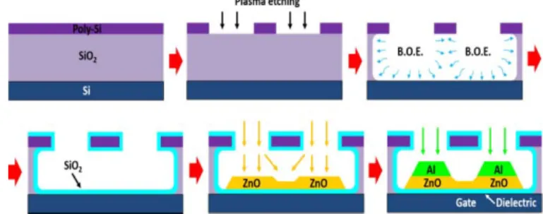
The process flow for fabricating ZnO TFTs is shown in Fig. 2. First, a 400-nm-thick SiO2and a 200-nm-thick poly-Si
Fig. 3. (a) Top-view SEM and (b) TEM images of a fabricated ZnO TFT. serving as the sacrificial layer and hard mask layer, respec-tively, were sequentially deposited by low-pressure chemical vapor deposition on an n-type Si wafer. After a photolitho-graphic step performed with an i-line stepper to generate photoresist-patterned S/D regions, the top poly-Si was etched by a reactive plasma etcher. Then, a selective wet etching using a buffer oxide etch solution was carried out to remove the underlying sacrificial SiO2. Due to the isotropic property of the wet etching, a suspended poly-Si bridge was formed and would serve as the shadow mask in the following steps. The gap height between the suspended bridge and substrate is defined by the thickness of sacrificial SiO2and is considered to have good uniformity and controllability. A 50-nm-thick SiO2 was subsequently deposited by PECVD under the pressure of 500 mtorr at 300 °C to serve as the gate dielectric. Then a 45-nm-thick ZnO film was deposited by a radio frequency sputter under a pressure of 5 mtorr at room temperature. In this step, due to the scattering of the sputtered species in the chamber, a self-assembled ZnO channel would form under the suspended bridge. Finally, the Al film was deposited by a thermal coater under the pressure about 8× 10⁻⁶ torr at room temperature to form the discrete S/D contacts and complete the fabrication of ZnO TFTs. To elucidate the importance of S/D metal contacts, some samples deliberately skip the Al deposition after forming the ZnO channel. The electrical characteristics of fabricated ZnO TFTs were measured with an HP 4156 parameter analyzer. Scanning electron microscopy (SEM) and transmission electron microscopy (TEM) were employed to observe the microstructure of the fabricated devices.
IV. RESULTS ANDDISCUSSION
Fig. 3(a) is the top-view SEM image of a fabricated device with L = 0.6 µm. It can be seen that a poly-Si bridge traverses the device area and separates the S/D regions. Fig. 3(b) is the TEM cross-sectional image of the device along line AB
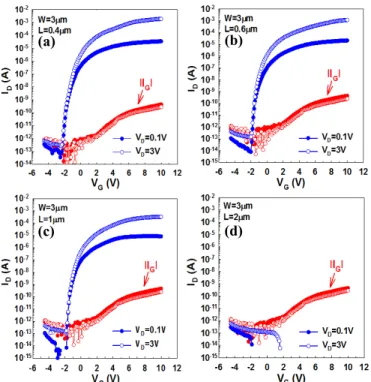
Fig. 4. Transfer characteristics of ZnO TFTs with L of (a) 0.4, (b) 0.6, (c) 1, and (d) 2µm. The applied drain biases are VD= 0.1 and 3 V. shown in Fig. 3(a). In this figure, we can see that both the gate oxide and ZnO films are continuous and have concave film profile. In addition, as expected, the two Al pads located at S/D regions are isolated from each other. Formation of desirable profile with various deposition tools is the key to the success of the FPE concept. The differences in the film profile of ZnO, SiO2, and Al are mainly ascribed to the different deposition circumstances for each material. Working pressure for the deposition of ZnO and SiO2 is in the order of 10−3 and 10−1 torr, respectively. In such high deposition pressures, scattering of deposited species is significant in the ambient and thus forming continuous film under the bridge.
Typical transfer characteristics of the ZnO TFTs with
L = 0.4, 0.6, 1, and 2 µm measured at VD = 0.1 and 3 V are shown in Fig. 4(a)–(d), respectively. Excellent electri-cal performance is obtained in terms of remarkable high ON-current, large ON-OFF ratio (>109), and low leakage current for devices with L equal to or less than 1 µm. The OFF-state current is dominated by the gate leakage, as shown in the figures. This is attributed to the rather large S/D-gate overlap areas (∼104 µm2) and the leakage is expected to be reduced as the structure is refined with a normal bottom-gate scheme [1]–[3]. Negligible drain-induced barrier lower-ing phenomenon was observed for the shortest device with
L = 0.4 µm. However, for the 2-µm device, there is no
turn-on behavior, while the drain current is contributed solely by the gate current. This is attributed to the disconnected channel that will be addressed in later discussion.
The very high ON-current exhibited in Fig. 4(a)–(c) is strongly related to the presence of Al metal contacts, which can effectively suppress the series resistances at S/D regions. To emphasize the significance of the metal contacts, we also made some devices without thermal-coated Al pads.
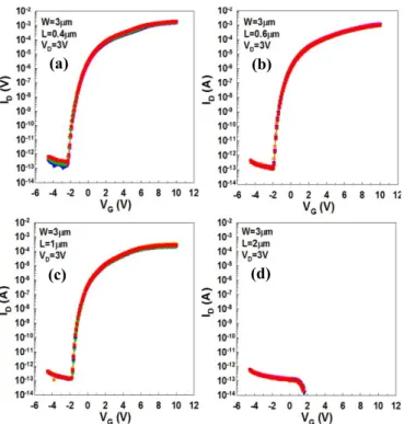
Fig. 5. Transfer curves of ZnO TFTs with and without self-aligned Al pads.
Fig. 5 is the comparison of electrical characteristics between the devices with and without the Al metal contacts. For the device without the Al pads, the probes put on the S/D regions were in direct contact with the ZnO film during the measurement. There is an offset region between the probe position and the channel, thus creating a situation similar to the drain-offset structure presented in [8]. As can be seen, the ON-current of device without Al metal contacts is several orders in magnitude lower than the one with Al metal contacts. In addition, unlike the one with Al metal contacts, the devices without Al metal contacts show anomalous operation behaviors that are obviously affected by the applied drain bias. The offset region mentioned above and the limited contact area between the probe and ZnO are responsible to the observation. According to [13], the overlapping area between the S/D metal pads and gate electrode plays a critical role in affecting the current spreading at the S/D sites. The less overlap between the S/D and gate will result in worse current spreading and higher parasitic resistance. Therefore, it is expected that the extremely high parasitic resistance would be produced in the fabricated devices without Al metal contacts in our work, leading to the poor characteristics shown in Fig. 5. The large series resistance also results in the increase in the turn-on voltage, similar to that reported in [8].
We have also checked the variation in the device charac-teristics of the fabricated devices and the results are shown in Fig. 6(a)–(d). Each figure in Fig. 6 contains data measured from five devices distributed in different dies on the wafer. The results confirm that excellent process uniformity can be achieved with the proposed method. Fig. 7(a) and (b) are the comparison of transfer characteristics between the devices with different L measured at VD = 0.1 and VD = 3 V, respec-tively. The electrical parameters extracted from the curves of
VD = 0.1 V are shown in Fig. 8. Very steep subthreshold swing (S.S.) lower than 200 mV/decade and high field-effect mobility (µFE) ranging from 21 to 45 cm2/V· s are obtained from the fabricated ZnO TFTs. The threshold voltages (VTH) extracted by constant-current method at W/L × 10−7 A are about 0.6 V. Moreover, it can be observed that the S.S. decreases with increasing L, while the turn-on voltage (VON)
shows opposite tendency. Fig. 9(a)–(c) are the output char-acteristics of the fabricated ZnO TFTs with L of 0.4, 0.6,
Fig. 6. Variation of fabricated devices with L of (a) 0.4, (b) 0.6, (c) 1, and (d) 2µm. Each figure includes five curves collected from five different dies.
Fig. 7. Comparison of transfer curves among devices with different L measure at VD= (a) 0.1 and (b) 3 V.
and 1µm, respectively. Good output properties with classical saturation behaviors are obtained except for the device with
L = 0.4 µm. This is attributed to the more significant
contribution of S/D contact resistance to the total resistance in the short-channel devices.
To explain these observations, TEM images, including the enlarged view taken at the channel center, of devices of various
L are checked, as shown in Fig. 10(a)–(d), respectively. Fig. 11
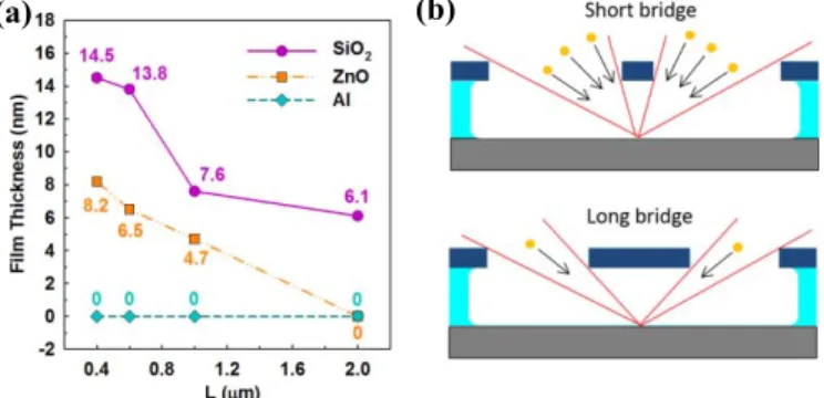
shows the film thickness of SiO2, ZnO and Al at the channel center extracted from the TEM images. The thicknesses of SiO2/ZnO of devices with L = 0.4, 0.6, 1, and 2 µm are 14.5/8.2, 13.8/6.5, 7.6/4.7, and 6.1 nm/0 nm, respectively. Obviously, both thickness of SiO2 and ZnO gets thinner as L becomes longer. This well explains the trends shown in
Fig. 8 that the device with a longer length displays more steep S.S. and more positive turn-on voltage. For the device with L of 2 µm shown in Fig. 10(d), the ZnO is found
Fig. 8. Electrical parameters obtained from curves shown in Fig. 7(a).
VON is defined to be the VG that ID starts to increase drastically. VTH is
extracted as the VG at ID= W/L × 10−7A.
Fig. 9. Output characteristics of fabricated ZnO TFTs with L of(a) 0.4, (b) 0.6, and (c) 1µm.
to be disconnected, the root cause why the devices of this dimension exhibit no turn-on behavior in Figs. 4(d) and Fig. 6(d). The decrease in film thickness with increasing
L is in part due to the more distinct shadowing effect of
the longer bridge, as shown in Fig. 11(b). In this aspect, the range of the incident angle for scattered species to reach the channel center under the bridge is wider for the device with a shorter L. This may potentially result in a thicker film at the channel center. Another major factor in affecting the profile is the directionality of the incident species as discussed in Section II. The directionality is affected by the configuration of the deposition tool as well as the process conditions-like deposition pressure. By adopting appropriate deposition tools and carefully manipulating the process conditions, the characteristics of the FPE devices can be ingeniously adjusted
Fig. 10. TEM images of ZnO TFTs with L= (a) 0.4, (b) 0.6, (c) 1, and (d) 2µm. Magnified image of the channel center is shown in the lower part of each figure.
Fig. 11. (a) Film thickness of SiO2, ZnO and Al at the channel center
of devices as a function of L. (b) Schematic picture to show the distinct shadowing abilities of bridges with a short or long L.
to match the requirements of practical circuitries. A scheme, which uses the FPE devices in the BEOL manufacturing of a chip [6] is shown in Fig. 12. Akin to [6] and [8], a planarized Cu interconnect and a SiN capping were used for the bottom gate and gate dielectric, respectively. After the formation of the suspended hardmask bridge, sputtered ZnO channel, and S/D metal contacts were deposited sequentially. The supe-rior device performance obtained in this paper evidences the feasibility of the FPE concept in practical applications.
Fig. 12. Integration of the FPE ZnO TFTs in the BEOL process of a chip.
V. CONCLUSION
In this paper, we propose a new FPE concept for the fabrication of oxide-based TFTs and based on it a novel one-mask process has been developed to fabricate ZnO TFTs. In the process, a suspended bridge was first built on the wafer by mature photolithographic and etch steps for shad-owing the deposited species in the follshad-owing deposition steps to tailor the profile of gate oxide, channel layer, and S/D contacts. This was done with the aid of different instruments with appropriate configuration and suitable process conditions. High-performance TFTs with submicrometer channel length, highly concave ZnO channel and S/D pads self-aligned to the suspended bridge were obtained through the proposed process. The fabricated ZnO TFTs demonstrate large ON-OFF ratio (>109), steep S.S. (71–189 mV/decade), low leakage current, and high field effect mobility (21–45 cm2/V· s). Excellent uniformity in the characteristics of the fabricated devices was also confirmed. Moreover, the electrical characteristics of devices with different L were also investigated. The devices with L = 2 µm fail to exhibit switching behavior as the deposited ZnO is discontinuous. For devices with L < 2 µm, the S.S. becomes steeper and turn-on voltage becomes more positive as L increases. This is attributed to the thinner gate oxide and channel films at the channel center, as verified by the TEM analysis. The thinner films were caused by the much severe shadowing effect of the longer bridge. The superior results obtained from the fabricated devices prove the FPE concept can be applied for practical TFT manufacturing.
REFERENCES
[1] E. Fortunato, P. Barquinha, and R. Martins, “Oxide semiconductor thin-film transistors: A review of recent advances,” Adv. Mater., vol. 24, no. 22, pp. 2945–2986, 2012.
[2] T. Hirao et al., “Review of recent developments in amorphous oxide semiconductor thin-film transistor devices,” Thin Solid Films, vol. 520, no. 6, pp. 1679–1693, 2012.
[3] T. Kamiya, K. Nomura, and H. Hosono, “Present status of amorphous In–Ga–Zn–O thin-film transistors,” Sci. Technol. Adv. Mater., vol. 11, no. 4, p. 044305, 2012.
[4] T. Hirao et al., “Bottom-gate zinc oxide thin-film transistors (ZnO TFTs) for AM-LCDs,” IEEE Trans. Electron Devices, vol. 55, no. 11, pp. 3136–3142, Nov. 2008.
[10] H. Sunamura et al., “High-voltage complementary BEOL-FETs on Cu interconnects using N-type IGZO and P-type SnO dual oxide semicon-ductor channels,” in Proc. Symp. VLSI Technol., 2013, pp. T250–T251. [11] H. C. Lin, R. J. Lyu, and T.Y. Huang, “Fabrication of high-performance ZnO thin-film transistors with sub-micrometer channel length,” IEEE
Electron Devices Lett., vol. 34, no. 9, pp. 1160–1162, Sep. 2013.
[12] A. Lu, J. Sun, J. Jiang, and Q. Wan, “One-shadow-mask self-assembled ultralow-voltage coplanar homojunction thin-film transistors,” IEEE
Electron Devices Lett., vol. 31, no. 10, pp. 1137–1139, Oct. 2010.
[13] S. Luan and G. W. Neudeck, “An experimental study of the source/drain parasitic resistance effects in amorphous silicon thin film transistors,”
J. Appl. Phys., vol. 72, no. 2, pp. 766–772, 1992.
Rong-Jhe Lyu received the B.S. degree from
National Chung Hsing University, Taichung, Tai-wan, and the M.S. degree from the National Tsing Hua University, Hsinchu, Taiwan, in 2009 and 2011, respectively. He is currently pursuing the Ph.D. degree in National Chiao in Tung University, Hsinchu, Taiwan.
He has been a Professor with the Department of Electronics Engineering, National Chiao Tung University, Hsinchu, Taiwan, since 1995.
![Fig. 1. (a) Top-view layout and (b) cross section [along the line AB in (a)] of the completed device](https://thumb-ap.123doks.com/thumbv2/9libinfo/7646285.138859/1.918.557.751.234.413/fig-view-layout-cross-section-line-completed-device.webp)