行政院國家科學委員會專題研究計畫 成果報告
應用統計與資料採掘技術以提昇晶圓製造良率之研究
計畫類別: 個別型計畫
計畫編號:
NSC91-2416-H-002-007-執行期間: 91 年 08 月 01 日至 92 年 07 月 31 日
執行單位: 國立臺灣大學工商管理學系
計畫主持人: 郭瑞祥
計畫參與人員: 陳正剛, 范治民
報告類型: 精簡報告
報告附件: 出席國際會議研究心得報告及發表論文
處理方式: 本計畫可公開查詢
中
華
民
國 92 年 8 月 13 日
2
行政院國家科學委員會專題研究計畫成果報告
應用統計與資料採掘技術以提昇晶圓製造良率之研究
The Application of Statistics and Data Mining Techniques to
Improving Semiconductor Manufacturing Yield
計畫編號:NSC 91-2416-H-002-007
執行期限:91/08/01 ~ 92/07/31
主持人:郭瑞祥 台灣大學工商管理學系
rsguo@ccms.ntu.edu.tw
共同主持人: 陳正剛 臺灣大學工業工程研究所
achen@ccms.ntu.edu.tw
摘要
當晶片尺寸愈小之時,半導體製造良率的
快速提昇亦愈形重要。如何從大量的製造資料
中有效偵測並診斷出良率損失,對半導體製造
商的競爭力愈益重要。
本研究旨在提出能從製造資料中自動萃取
出製程錯誤診斷的重要知識,並提出一整合性
的參數分析與圖形輔助技術,整合統計品質管
制、資料採掘、製程知識,以提昇多階段製程
整合的良率。
本整合技術包含了變異分解、主要參數過
濾、線性模式建立、圖形輔助診斷與監控法則
修改五大步驟。藉由實際資訊的測試,驗證了
本方法能輔助工程師診斷錯誤原因,因而提昇
良率。
關鍵詞:良率提昇、統計模式、資料採掘
Abstract
Ramping up yield in semiconductor
manufacturing is getting more difficult as the
feature size of IC device continuously shrinks
down. How to efficiently detect and diagnose the
yield loss from the mass volume of manufacturing
data is becoming critical to enhance a
manufacturer’s competition capability. In this
research, we focus on techniques for
automatically extracting process knowledge from
production database for fault diagnosis and
optimizing device performance with fixed target.
An integrated parametric analysis scheme is
developed with supplemented graphical methods
to facilitate interpretation of results. It consists of
five phases: Device Variation Partition, Key Node
Screening, Linear Equipment Modeling, Graph
Aided Interpretation, and Control Policy
Re-evaluation. The concepts of quality control,
data mining, and process knowledge are
integrated in this scheme. Field data case study
shows that the integrated parametric analysis
scheme is able to diagnose the parametric yield
problem, help engineers construct the knowledge
base, predict the yield, and provide insights for
yield enhancement.
Keywor ds: Yield Improvement, Statistical Model,
The Application of Statistics and Data Mining Techniques to
Impr oving Semiconductor Manufactur ing Yield
Ruey-Shan Guo Dept of Business Administration
National Taiwan University Taipei, Taiwan Abstract –This research focuses on techniques for automatically extracting process knowledge from production database for fault diagnosis and optimizing device performance with fixed target. An integrated parametric analysis scheme is developed with supplemented graphical methods to facilitate interpretation of results. It consists of five phases: Device Variation Partition, Key Node Screening, Linear Equipment Modeling, Graph Aided Interpretation, and Control Policy Re-evaluation. The concepts of quality control, data mining, and process knowledge are integrated in this scheme. Field data case study shows that the integrated parametric analysis scheme is able to diagnose the parametric yield problem, help engineers construct the knowledge base, predict the yield, and provide insights for yield enhancement.
INTRODUCTION
Ramping up yield and quality in semiconductor manufacturing is getting more difficult as the feature size of device continuously shrinks down. How to efficiently detect and diagnose the yield and quality issues from the mass volume of manufacturing data is becoming critical to enhance a manufacturer’s competition capability. Design of experiments and powerful analysis tools provided by Engineering Data Analysis (EDA) system have provided a solid basis for a well tuned manufacturing process. However, conducting either of them is time consuming and tedious for a multi-stage process analysis. Additional tools are needed to solve the complex problems faster.
“Data Mining” has emerged as a new tool to support the rapid yield improvement efforts. It is a collection of methods for automatically extracting buried information and rules from enormous data. For example, Fujitsu and Motorola adopt “decision tree” and “self-organization neural network” respectively to identify the critical yield factors from the normally collected wafer manufacturing data [1][2]. These methods are powerful in detecting the hidden trends and providing the capability to understand patterns of behavior when the relationships are not known. Although data mining techniques have been proved to be useful for semiconductor manufacturing, each of them has its own inherent pros and cons. Table 1 lists the comparison of several techniques such as decision tree, neural network, and traditional regression/ANOVA methods which are
commonly adopted for semiconductor manufacturing analysis [3]. It can be seen that the major advantages of data mining techniques over the regression/ANOVA method is that they do not need a pre-defined model. However, the decision tree technique is less useful when we want to make more precise predictions for a continuous variable, and the neural network technique is difficult to make a physical interpretation of the models.
This research intends to combine the advantages of both standard statistical methods and modern data mining techniques. In specific, an integrated parametric analysis scheme sequentially adopting the techniques of decision tree and regression/ANOVA is developed. The analysis results of this scheme are easy for physical interpretation with the aid of statistical graphs. Also, it is designed to provide the capabilities of fault diagnosis, quality improvement, yield prediction, and knowledge base construction.
In the following sessions, both issues and
functions of the integrated parametric analysis
scheme are first addressed. Then the various
phases in this scheme are applied to the field data
from a local foundry fab for case study purpose.
INTEGRATED PARAMETRIC ANALYSIS SCHEME
From the viewpoint of process integration,
statistical stability of the process at the in-line
level does not guarantee that of the end-of-line
parametric data. First of all, not all the process
parameters are clearly identified, and furthermore
not all the dependencies among process
parameters are considered in the in-line process
control. There should be a way for on-line
monitoring of processing equipment from the
“integration” level, i.e., based on the end-of-line
parametric yield performance.
The integrated parametric analysis scheme
provides this capability by two steps:
(s1) Decompose the parametric variation into hierarchical levels of variation component such as lot-to-lot, wafer-to-wafer, and across-wafer variation.
(s2) Estimate the contribution of individual equipment on each hierarchical variation component extracted from the first step.
However, there are many equipment effects to be
extracted and these equipment effects will change
dynamically with time. Therefore, in addition to
the statistical methods, the integrated parametric
analysis scheme also incorporates with “data
mining” techniques to solve these problems. As
demonstrated in Fig. 1, the scheme consists of
five phases: Device Variation Partition, Key Node
Screening, Linear Equipment Modeling, Graph
Aided Interpretation, and Control Policy
Re-evaluation.
Device Variation Partition
The major function of this phase is to decompose
the end-of-line parametric variation into
hierarchical variation components. Both mean
and variance effects of lot as well as wafer level
are estimated. It adopts Multi-vari method [4] and
Variance Component Analysis [5] in this phase.
Key Node Screening
Once the parametric variation components are
extracted, the next step is to apply data mining
techniques to explore the large space of
explanatory factors. In specific, the decision tree
technique is adopted to identify the critical
process steps and corresponding equipment for
in-depth analysis.
Linear Equipment Modeling
To further construct the relation between the
end-of-line parametric data and individual
equipment, an empirical modeling technique is
developed. The possible candidates for the
explanatory factors are selected in the previous
phase to achieve the goal of using the fewest and
simplest possible factor combination. The Linear
Equipment Modeling (LEM) is derived by
expanding the functional relationship with a
first-order additive model. To capture the
dynamic trend in explanatory factors, the time
period is also considered as an explanatory factor
in LEM. For example,
i P p mip tip i X e Y = + ∑ + =1( ) ) , ( ), , ( µ (1) where
Y is an parametric variation component at lot level, i is the lot ID,
p is the critical process step ID,
P is the total number of critical process steps,
m(i, p) is the equipment ID processing wafer i in step p, t(i, p) is the time period wafer iprocessed in step p, µ is the long-term mean of Y,
Xm(i,p),t(i,p) is the effect of equipment m(i, p) at time period t(i,p),
e
iis modeling residual.
Graph Aided Interpretation
To facilitate the interpretation of the extracted equipment effects from LEM, several statistical graphs are used: (g1) Normal probability plot: help engineers quickly
identify the abnormal equipment.
(g2) Mean/variance plot: provide clues for rapid diagnosis and robust feedback control.
(g3) Trend (control) chart: enable the continuous monitoring of stability of equipment from an integration point of view.
Control Policy Re-evaluation
Daily or weekly running of the integrated parametric analysis scheme provides an opportunity to discover the underlying process model and evaluate the in-line process control policy from an integration point of view. Based on the “dependency” between the in-line parameters and the extracted equipment effects from LEM, the following scenarios are considered:
(c1) If the dependency is strong, it can be used for setting the reliable in-line SPEC.
(c2) If there exists no significant dependency, try to re-evaluate the in-line sampling strategy. We can either enhance the sampling strategy for increasing sensitivity or reduce the sampling size/rate for cost down.
(c3) If the dependency is changing, dynamically increase the sampling size/rate for rapid estimation of new dependency, and try to find out the root cause and include the new model into the knowledge base.
FAB DATA CASE STUDY
Due to the limit space, this paper skips the Device
Variation Partition phase and directly uses the lot
mean sequence of P+ contact resistance, Rc_P+,
coming from a local foundry fab as an example.
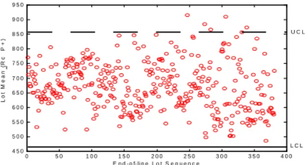
In this case study, the parameter Rc_P+ was
detected to be out of control limit around the
250
thlot. Fig. 2 illustrates the end-of-line control
chart of Rc_P+.
Key Node Screening: With the help of decision tree technique, the equipment in photo, etching, sputtering, and rapid thermal annealing process steps are quickly identified as the critical factors. Fig. 3 shows the decision tree
extracted from the data in week 15. As can be seen, it provides an easy comparison among the equipment mean effects and we can observe that ACON2 has a higher Rc-P+ effect than that of ACON3 (and ASPU6 > ASPU8, APHO4 > APHOG, AIMD1> AIMD2).
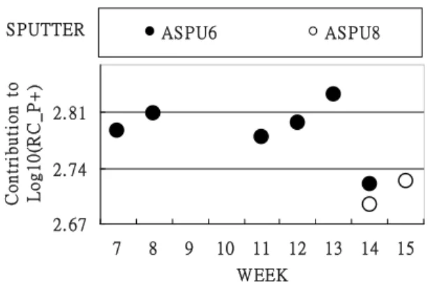
Linear Equipment Modeling: Then LEM technique is applied to the data set and the fitted regression model has a R-Square of 0.80. Fig. 4 is the observed vs. predicted plot. Graph Aided Interpretation: As shown in Fig. 5, the normal probability plot of the estimated mean effects clearly shows that there are many significant equipment mean effects. Fig. 6 illustrates the candidate LEM explanatory factors selected by the decision tree method and the estimated equipment mean effect in week 15. It clearly shows the contribution of “individual” equipment to the parametric lot mean, which is different from the “combinational” equipment effects as estimated in the decision tree method (Fig. 3). Fig. 7 and 8 also show the trend charts of these equipment mean effects from week 7 to week 15. They are useful for continuous monitoring purpose.
Based on the combined use of decision tree method and LEM technique, we were able to find out the root cause. As shown in Fig. 7, the equipment mean effect of Rc-P+ has an upward shift in week 11 at equipment ACON3 (etching tool). Also in Fig. 8 the equipment mean effect of Rc-P+ has an upward shift in week 11 at equipment ASPU6 (sputtering tool). To trace the root causes of “upward” shift of Rc_P+ contributed by ASPU6, we also plot the trend chart of in-line Ti measurements taken from ASPU6. As shown in Fig. 9, the in-line measurements of Ti thickness “drop” significantly in week 11. It is a surprise to us since this observation is in contrast to the physical rule that Rc_P+ should be proportional to the Ti thickness,
Rc_P+ = k˙hTi / w (2)
where hTi is the deposited Ti thickness, w is the contact
window size after etching inspection, and k represents the contribution from other terms.
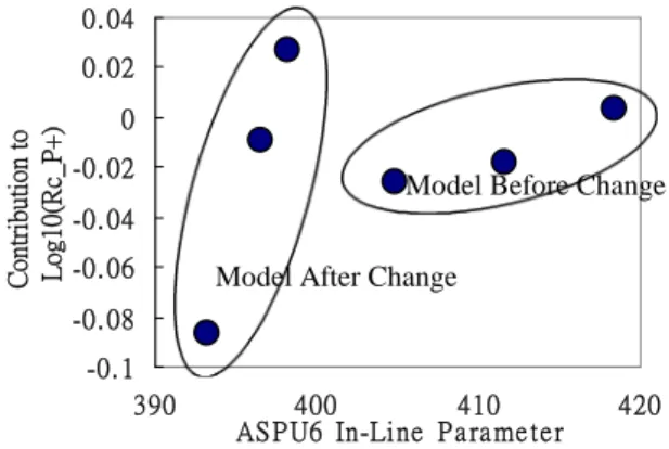
To explain the result, an investigation was performed. It was found that the upward shift of the mean effect of ACON3 was caused by a drop of contact window size. This change also changed the relationship between the in-line thickness and equipment effect of ASPU6. Fig. 10 shows the scatter plot between Ti thickness and Rc_P+ contributed by ASPU6. As can be seen, the model after the “upward” shift of equipment ACON3 had a larger slope compared to the slope before the change. As a result, we observed a higher ASPU6 mean effect even after the drop of the Ti thickness.
Control Policy Re-evaluation: Based on the observation in Fig. 10, reducing the upper specification limit of Ti layer thickness hTi at the sputtering tool, ASPU6, would be useful
in compensating for the upward shift occurred at the
previous etching tool, ACON3. CONCLUSIONS
The integrated parametric analysis scheme combining statistical control methods with modern data mining techniques is developed and studied using the fab data. It provides a new approach of continuous monitoring of in-line processing equipment from the viewpoint of process integration. More applications based on this scheme such as identification of equipment combination effects, yield prediction, robust feedback and feed-forward control, and knowledge base construction will be reported in the near future.
REFERENCES
[1] H. Tsuda, H. Shiri, O. Takagi and R. Take, “Yield analysis and improvement by reducing manufacturing fluctuation noise,” p249 – 251, ISSM 2000 proceedings.
[2] R. M. Gardner, J. Bieker, and S. Elwell, “Solving tough semiconductor manufacturing problems using data mining,” p46 – 55, ASMC 2000 proceedings. [3] R. Kittler and K. Wang, “The emerging role of data
mining,” Solid State Technology, p45-58, vol. 42(11), 1999.
[4] L.A. Seder, “Diagnosis with diagrams,” Industry Quality Control, vol. 6(4), 1950.
[5] C. Min, R. Guo, S. Chang, and J. Wei, “SHEWMA: an end-of-line SPC scheme using WAT data,” IEEE Trans. on Semiconductor Manufacturing, August 2000.
Regression/
ANOAV
Decision
Tree
Neural
network
Model
free
ˇ
ˇ
Robust to
outliers
ˇ
Physical
interpretation
ˇ
ˇ
Continuous
outputs
ˇ
ˇ
Discrete
outputs
ˇ
ˇ
ˇ
Device Variation Partition Key Node Screening
Linear Equipment Modeling
Graph Aided Interpretation Control Policy Evaluation
Manufacturing Process Hierarchical Variation Components Critical Process Equipment Mean Variance Effect Probability Plot Mean/Variance Plot Control Chart End-of-line Parametric & Manufacturing Data In-line SPEC/ Sampling Evaluation & Feedback/forward Control
Table 1: Comparison among data mining
techniques
Fig. 1: Integrated parametric analysis scheme
Fig. 2: End-of-line control chart of Rc_P+
0 5 0 1 0 0 1 5 0 2 0 0 2 5 0 3 0 0 3 5 0 4 0 0 4 5 0 5 0 0 5 5 0 6 0 0 6 5 0 7 0 0 7 5 0 8 0 0 8 5 0 9 0 0 9 5 0 E n d - o f- l i n e L o t S e q u e n c e Lo t M e an ( R c P + ) U C L L C L
Fig. 3: Decision tree of Rc_P+
Fig. 4: The observed-vs.-predicted plot of Rc_P+
2 . 6 5 2 . 7 2 . 7 5 2 . 8 2 . 8 5 2 . 9 2 . 9 5 3 3 . 0 5 0 . 0 0 1 0 . 0 0 3 0 . 0 1 0 . 0 2 0 . 0 5 0 . 1 0 0 . 2 5 0 . 5 0 0 . 7 5 0 . 9 0 0 . 9 5 0 . 9 8 E q u ip m e n t M e a n E ffe c t P ro b a b il it y S p u t t e r A S P U 6 8 2 6 E t c h i n g 4 . 4 2 P h o t o A C O N 2 2 A P H O 4 8 1 0 . 6 2 8 3 2 . 4 4 1 0 . 3 6 S p u t t e r 2 8 . 0 2 5 A S P U 8 2 8 0 0 . 3 7 5 0 . 7 5 P h o t o 3 A P H O G 7 3 6 . 3 1 # 1 R c _ P + P h o t o L o t M e a n A P H O 4 W e e k 1 5 5 9 1 . 6 4 S p u t t e r 1 0 . 2 1 A S P U 6 2 5 8 0 . 1 3 1 8 . 2 9 P h o t o 3 A P H O G 5 5 7 . 1 1 # R T A E t c h i n g 1 A I M D 1 A C O N 3 6 0 7 . 3 7 5 5 9 . 4 3 P h o t o # 3 2 . 2 4 A P H O 4 1 1 0 5 7 3 . 6 2 2 6 . 6 9 R T A 4 A I M D 2 5 6 2 . 2 7 S p u t t e r 2 0 . 8 5 A S P U 8 3 5 5 0 . 5 5 3 5 . 6 2 R T A 7 A I M D 1 5 2 4 . 7 9 P h o t o 2 1 . 3 8 A P H O G 2 5 1 9 . 8 1 8 . 8 3 R T A 3 A I M D 2 5 0 9 . 8 1 # 1 Node Definition Step Name Equipment ID Mean Value Standard Deviation Number of Lot
Fig. 5: Probability plot of equipment mean effect
Fig. 6: Rc_P+ equipment mean effect
Fig. 7: Etching equipment mean effect ETCHING 2. 81 2. 88 2. 95 7 8 9 10 11 12 13 14 15 WEEK C o n tr ib u ti o n t o L o g1 0( R C _ P + ) ACON 3 ACON 2 S PUTTER 2. 67 2. 74 2. 81 7 8 9 10 11 12 13 14 15 WEEK C o n tr ib u ti o n t o L o g1 0( R C _ P + ) AS PU6 AS PU8 M ea n E ff ec t o n L o g 1 0 (R c_ P + ) 550.0 676.3 802.6 A P H O 4 A P H O G A C O N 2 A C O N 3 A S P U 6 A S P U 8 A IMD 1 A IMD 2
Fig. 8: Sputtering equipment mean effect
Fig. 9: Trend chart of ASPU6 Ti thickness measurements
Fig. 10: Scatter plot of in-line Ti thickness and the contribution of ASPU6 on Rc_P+ mean 385 400 415 9 9 10 10 11 11 12 13 13 14 14 15 WEEK A S P U 6 I n-L ine P a ra m e te r -0. 1 -0. 08 -0. 06 -0. 04 -0. 02 0 0. 02 0. 04 390 400 410 420 AS P U6 In-Line P a ra me te r Contribution to Log10(Rc_P+)
Model Before Change