Single-Stage Push–Pull Boost Converter
With Integrated Magnetics and Input
Current Shaping Technique
Rong-Tai Chen and Yung-Yaw Chen
Abstract—This paper presents a novel single-stage push–pull
boost converter with improved integrated magnetics and a better low-ripple input current. Most of the reported single-stage power factor corrected (PFC) rectifiers cascade a boost-type converter with a dc–dc converter. It is found that the push–pull converter, when the duty cycles are greater than 50%, can simplify the front end of the boost-type converter to a novel single-stage converter. Coupled inductor techniques provide a method to reduce the converter size and weight and to achieve a ripple-free current. All the magnetic components including the input filter inductor and the step-down transformer are integrated into a single EI core. The proposed integrated magnetic structure has a simple core structure, a small leakage inductance, and low core losses. The prototype is built to demonstrate the theoretical prediction.
Index Terms—Integrated magnetics, push–pull boost converter,
ripple-free, single-stage.
I. INTRODUCTION
I
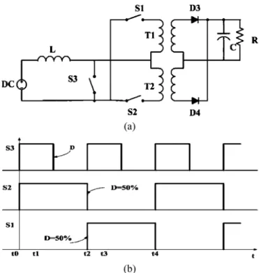
N RECENT years, a number of single-stage input current shaping converters have been introduced in [1]–[5]. It is found that many of these topologies can be implemented by combining a two-terminal or three-terminal boost input current shaper cell with dc–dc converter along with an energy storage capacitor in between [6], [7]. This capacitor must be realized by a conventional power component with high current stress. The major disadvantages of the conventional two-stage conver-sion approach are the added cost, the high current stress, and the complexity of the two-control loop two-power-stage nature. The single-stage power factor corrected (PFC) ac/dc converters integrated the two power stages into one, thus reducing signifi-cantly the component count and cost and gaining much attention in many low-power applications during the past ten years.Fig. 1(a) shows the preregulated dc–dc boost converter with a parallel dc transformer. The switching power circuit (SPC) uses three main switch elements. The two converters are con-trolled independently to achieve output voltage regulation. The duty cycles of the switches , , and are 50%, 50%, and , respectively. The duty ratio may be larger or less than 50%. Fig. 1(b) shows the switching sequence of the three main-switches. In a general sense, the two main switches of the tra-ditional push–pull converter operate alternately, with
conduc-Manuscript received July 28, 2004; revised May 11, 2005. This work was presented at the 35th IEEE Power Electronics Specialists Conference, Aachen, Germany, June, 2004. Recommended by Associate Editor Y.-F. Liu.
The authors are with the Department of Electrical Engineering, National Taiwan University, Taipei 106, Taiwan, R.O.C. (e-mail: rtchen@ipmc.ee.ntu. edu.tw).
Digital Object Identifier 10.1109/TPEL.2006.880353
Fig. 1. Preregulated dc–dc boost converter. (a) Power circuit. (b) Switching sequences withS1 and S2 duty ratio equal to 50%.
tion duty cycles of 50% during one complete switching cycle. These switching actions generate a symmetrical and alternating voltage across the primary of transformer. It is found that the push–pull converter, when the duty cycles greater than 50%, leads to conduct overlap intervals. Conduction overlap of pri-mary switches causes high current spikes during such intervals. If the transformer is supplied from a voltage source and both switches are ON simultaneously, there is very little impedance to limit the switch current amplitudes and the switches could very well be damaged or destroyed as a result. A boost converter is added to the front end of the conventional push–pull converter for PFC as shown in Fig. 1(a). Thus, the possibility of damage is removed. The energy stored in the input inductor follows any overlap interval of two switches. At the next interval, the en-ergy is delivered to the output network. One of the advantages of the overlapping primary switch conduction is the equal divi-sion of the inductor current in two switches, thus reducing their average and rms current levels as well as the primary winding rms current magnitude. When MOSFET devices are used as the switch elements, a significant improvement in conversion effi-ciency can be achieved.
An application of the zero-ripple technique to converter struc-ture is described in [8]. In this paper, the zero-ripple technique is applied to the proposed push–pull converter. For basic consider-ation, it seems to be perfect that only by extending a basic con-verter structure by a defined magnetic coupling of the input and filter inductors can a complete elimination of the input current ripple be obtained. It is shown that the ripple suppression can be achieved only on the input side or on the output side. A cir-cuit consisting of passive elements cannot have an infinite high effective input inductance for all frequencies. The impossibility of a complete suppression of the input current ripple of the con-verter becomes clearly understandable. Therefore, the system should be labeled better low-ripple boost converter and not zero-ripple boost converter. In addition, coupled inductor techniques supply a method to reduce the converter size and weight and to achieve ripple-free current. In order to improve efficiency and reduce size, this paper proposes an improved push–pull boost converter with integrated magnetics. In this structure, all the magnetic components including input inductor, input filter in-ductor, and step-down transformer are integrated into a single EI core. The proposed integrated magnetic structure has a simple core structure, a small leakage inductance and low core losses. The prototype is built to demonstrate the theoretical prediction. This paper is organized as follows. Section I introduces the research background and the motivation of this work. Section II briefly reviews basics considerations. Section III proposes an improved push–pull boost converter with integrated magnetics. Section IV provides experimental results.
II. PRELIMINARYCONSIDERATION
In order to clearly explain the proposed converter, we want to consider the primary concepts in the following.
A. Single-Stage
There are several interesting state-of-the-art single-stage so-lutions [1]–[5]. Single-stage soso-lutions supply the load with a constant and fast-regulated dc voltage, while in most cases the line current is not sinusoidal. The pulsed current deteriorates the line voltage, produces radiated and conducted electromagnetic interference, and leads to poor utilization of the capacity of the power sources. For single-phase electronics applications, pas-sive power filters, active one and two-stage PFC rectifiers are typical approaches used to achieve high power factor and low total-harmonic distortion (THD). Compared with the two-stage approach, many strategies have been developed to reduce the size and the cost and to improve the efficiency.
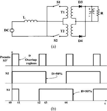
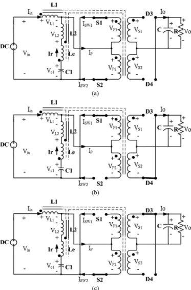
In this paper, an improved boost-derived push–pull converter is proposed as shown in Fig. 2(a). It is found that the push–pull converter, when the duty cycles are greater than 50%, can op-erate in an interesting condition. Therefore, it acts as a combi-nation of the front end of the boost-type converter and a novel single-stage converter.
If the duty cycles of and are made variable and always greater than 50%, and it can be eliminated, as shown in Fig. 2(a); i.e., if and have overlapping conduction interval, then is no longer needed. Fig. 2(b) shows the switching sequences of the two main switches and a pseudo switch . As a result, the proposed single-stage push–pull boost converter as shown in Fig. 3(a) integrates a ripple-free input current shaper and
Fig. 2. Improved boost-derived push–pull converter. (a) Power circuit. (b) Switching sequences withS1 and S2 duty ratio greater than 50%.
an isolated push–pull converter with two shared switches and controllers. One of the advantages of the overlapping primary switch conduction is the equal division of inductor current be-tween and , thus reducing the switch stress and improving conversion efficiency. The proposed push–pull boost converter in Fig. 3(a) with the duty cycles greater than 50% is a suitable approach for ripple-free input current. Fig. 3(b) shows the main typical waveforms of the converter in a switching cycle. This will be verified in the following sections.
B. Ripple-Free Input Current
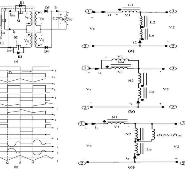
In order to explain the effect called zero-ripple phenomenon in Fig. 3(a) [8], we want to consider briefly the relationships given for magnetic coupling of the two ports networks shown in Fig. 4(a). The two ports network is part of Fig. 3(a), and the nodes are indicated by , , and . Fig. 4(b) is the equivalent circuit of Fig. 4(a) which is represented by an ideal transformer ( ) and a mutual inductance , where
under ideal conditions. The elimination of the ideal transformer from Fig. 4(b) results in the simple model of Fig. 4(c) by trans-formation from the primary to the secondary side. The sec-ondary equivalent inductance is . The following mathematical deriving from Fig. 4(c) is used to analyze the ripple cancellation [9], [11], [12].
Let us now make the assumption that it is possible to reduce the value of to zero in our model as shown in Fig. 4(c); and let us examine the circuit currents and voltages that result from our assumption. If is zero, then the ac voltage drop across must also be zero, as illustrated in Fig. 4(a). The voltage appearing across must therefore be equal to that of the sec-ondary voltage source, , reflected through the ideal transformer in the model. Also, the current through and must be equal to that produced by the secondary voltage,
Fig. 3. Proposed push–pull boost converter. (a) Power circuits. (b) Main typical waveforms.
. These conditions lead to the simplified circuit model of Fig. 3(c), where
(1)
(2)
(3)
The relationship between secondary leakage inductance and that of the core material set by (3) is important and worth dwelling on for a moment. First of all, recall that this equation was derived based on the premise that no input ripple current existed in our model and, if satisfied, must produce this con-dition. It is known that there are several advantages to having and wound on the same core. One viable method is to tightly wind primary and secondary turns together to reduce the leakage inductance of and to essentially zero, and then insert a small external trimming inductor in series with the secondary sides to emulate the desired value of .
Fig. 4. Two-port network of the magnetic coupling. (a) Proposed coupling in-ductor. (b) Equivalent circuit of (a). (c) Equivalent circuit of (b).
The initially analyzed basic principle of ripple elimination can now be applied to the proposed push pull converter. A cou-pling capacitor has to be provided in order to suppress the occurrence of a dc voltage component across . If the capaci-tance is selected sufficiently large, identical voltages across and will result. The zero-ripple phenomenon will be ob-tained only for the theoretical limiting . Therefore, the assumptions mentioned in Fig. 4 are present for suppressing the ripple of the input current by proper choice of the . For a practical system realization a capacity value as small as pos-sible is desired in order to minimize size and weight of the con-verter. The average value of the coupling capacitor is equal to the input voltages in the stationary case. That is, . Then, that follows for a small finite ripple of the input current 2 results. It acts like a low-pass filter lying at the converter input.
One has to point out that the low-pass filter is already an inte-gral part of the basic converter structure. Thus, it does not have to be realized by additional power components; however, for the conventional boost converter acts as an essential element of the energy transfer between the input and output sides. There-fore, the current stress on is basically different from that of a
Fig. 5. Discrete magnetics of the proposed push–pull converter
Fig. 6. Integrated magnetics of the proposed push–pull converter.
conventional filter capacitor. A circuit consisting of passive el-ements , , and cannot have an infinitely high effective input inductance for all frequencies. Thus, a complete suppres-sion of the input current ripple is impossible. The system shown in Fig. 3(a) should be labeled a better low-ripple converter and not a zero-ripple converter.
C. Integrate Magnetics
From Fig. 3(a), the magnetic core requires inductive elements like , , and transformer , . The SPC circuits of Fig. 5 are discreted magnetic versions of boost and push–pull topolo-gies with transformer isolation. Let us now see if we can for-mulate an easy way to synthesize an integrated magnetic ver-sion of Fig. 6, given the discrete-magnetic circuit arrangements as starting points. To begin, we must first reconstruct the cir-cuit schematics of Fig. 5 so as to detail the magnetic aspects of the transformer and inductor components. The schematics along with the result from this reconstruction process are illustrated in Fig. 6. Note that a flux direction within each magnetic compo-nent has also been assigned, based on winding polarities pro-duced by converter operation. Next, for each of the switching intervals of the converters, a set of equations defining the rate of change of flux in each magnetic component is established [12]. For this exercise, we can assume all semiconductors of the SPCs are ideal in order to simplify our work. Also, we will ig-nore potential leakage inductance effects between transformer windings for the same reason, and assume that fluxes are com-pletely contained within its core structure.
Thus, for the converter of Fig. 5 during interval I ( )
(4)
For the converter of Fig. 5 during interval II ( OFF) (5)
(6) From (5) and (6), we can combine them to eliminate the de-pendent variable, . Performing this combination gives
(7)
Note that the last term of (7) is of a form that could be con-sidered as defining a flux change in a magnetic medium that is dependent on the input voltage, , of the converter and the number of primary turns on the converter’s transformer, . Since our goal is to make the inductor a part of the same mag-netic assembly that contains the transformer component, it is logical to assume that should be made equal to , so that all of the flux change is contained within one magnetic path or leg of this assembly. Therefore, we arrive at an expression for
as
(8) We can interpret (8) as defining a magnetic assembly in which there are three major flux paths. It also tells us that the flux change in an input source-related path contributes to the change in another path associated with the inductor portion of the magnetic assembly , as well as to flux change in a third path . These general observations permit us to sketch out a magnetic path arrangement that satisfies the needs of (8). This is done in Fig. 6. It shows the flux distribution in the core. The transformer and the filter inductors in the push–pull boost converter can be integrated into a single magnetic core. Note that we have added a gap in the inductor path area because we expect this leg will have significant dc bias, just as a discrete inductor in a boost converter would experience.
In order to improve the core structure and to reduce the leakage inductance of the existing integrated magnetics, a novel magnetic integration approach is proposed in [10]. First, since the transformer’s primary winding is split between two outer legs, as shown in Fig. 6, interleaved windings can be used to minimize the leakage inductance of the integrated transformer. Second, the polarity of one set of windings is changed through different winding connections. Correspondingly, the direction of flux is changed as well. The air gap on the center leg prevents saturation of the core. The air gap will be the major factor in determining their winding inductance values, and increasing the air gap length will decrease the inductance of a magnetic material. Third, as shown in Fig. 6, auxiliary windings can be added to the center legs of the integrated magnetic converters to reduce input ripple current magnitudes. We can utilize the transformer equations of (3) to select the number of turns of this third winding so as to adjust the SPC’s input current ripple to essentially zero. The gap inductance (Lg) is much smaller than that of the ungapped outer legs of the magnetic structure. Both center leg winding are wound tightly together to maximize magnetic coupling between them and to minimize
parasitic leakage inductances. The addition of this second winding does not compromise the input-to-output voltage gain of the converter, and it is defined in the following.
III. PROPOSEDPUSH–PULLBOOSTCONVERTER
The proposed push–pull converter with integrated magnetics is studied in this section. It can achieve continuous or better low-ripple input current with duty cycle greater than 50%. This section mainly discusses the steady-state and integrated mag-netic properties of the proposed converter. It shows that the pro-posed boost converter has the same steady-state properties as the conventional boost converter. The prototype is built to demon-strate the theoretical prediction.
A. Principle of Operation
In boost-derived push–pull converters as shown in Fig. 3(a), switch duty cycle (D) is greater than 50% and a separate drive circuit will be necessary for each dc isolated switch element. The two switch elements have conduction duty cycles greater than 50%. Twice during each switching cycle, the two main switches are ON simultaneously. At the beginning of a switching cycle, and are ON. Inductor current therefore flows through and . Energy to sustain the output voltage load comes from the filter capacitor . When turns OFF and switch closes, it now allows the inductor current to flow through the primary of and to deliver its stored energy to the output of the converter. One conversion stage consists of switches , transformer , diode , and rectifier diode . The other one consists of switches , transformer , diode , and rectifier diode . In addition, a two-port magnetic coupling cell is used for the input filter. is the small leakage inductance of the coupled inductor. In order to prevent parasitic ringing and negative undershoots across and , caused by parasitic capacitance of and , low current stress diodes
and are used.
The switching sequences and theoretical waveforms of the proposed converter are illustrated in Fig. 3(b). As shown in Fig. 3(b), the switching sequence differs from that of universal push–pull converters. and are driven complementary with an overlap interval (mode 1). The output voltage can be regu-lated by varying this controllable interval as pulsewidth mod-ulation (PWM) with a constant switching frequency. The prin-ciple of operation in a steady-state condition is described with the following assumptions.
• All the switches and components are ideal. • Transformers and are identical.
• Inductance and are tightly coupled with each other. • The output voltage is assumed to be constant.
1) Mode 1 ( , ): With switches
and ON as shown in Fig. 7(a), the inductor is grounded. The input current, is increased, resulting in energy stored in . The current through , is increasing and then changes its direction. Diodes and are not conducting during this period. The voltage across inductor is the input voltage, , and the voltage across inductor is .
2) Mode 2 : With switch ON and
OFF as shown in Fig. 7(b), releases the energy stored in to the transformer . is still keeping its positive direction;
Fig. 7. Principle of operation circuits: (a) Mode 1, (b) Mode 2, and (c) Mode 3.
however, it is decreasing. The capacitor is charged by . The voltage across inductor is ( – ). The voltage across
inductor should be .
3) Mode 3 : With switch OFF and ON
as shown in Fig. 7(c), releases the energy stored in to the transformer . The converter action operates the same as mode 2.
As a result, the inductances and have the same voltage waveforms during the whole cycle. It is possible to couple them and to achieve a reduced component count, reducing the amount of material, increasing the energy density, and achieving ripple-free input current [8]. The voltage relationships of Fig. 6, along with the right choice of leakage inductances ( ) associated with the inductor windings, are the key factors in achieving zero-ripple current at the input of the proposed push–pull converter.
The meanings of variables in this paper are listed in Table I.
B. Steady State Analysis
1) Voltage Gain: According to the voltage-second balance
where
(10)
Thus, the following voltage gain can be derived
(11)
Considering the power balance , that is
(12)
The current gain is
(13)
2) DC Characteristics: From Fig. 6, the average current of
and can be derived as follows:
(14)
(15)
It can be seen that the presence of the capacitor implies that 0 in steady state. and are defined as follows:
(16)
(17)
The output average current flows in mode2 and mode3, i.e., when the diode is conducting. Therefore
(18)
Using the assumption of 100% efficiency, the average input current can be derived
(19)
Summing and
(20)
An interesting equation can be derived
(21)
This means that the averaged input current is equal to the sum of the currents through the two inductors.
Qualitatively, this must be true since 0.
3) Boundary Condition: Considering the power balance
again, where
(22) (23) Thus
(24)
then substituting (17) into (24), that is
(25)
It can be seen that continuous current mode can be achieved in the proposed topology. The boundary conditions are
(26)
(27) (28)
4) Semiconductor Devices Stress: The switch average
cur-rent is
(29)
The diode average current is
(30)
The switch peak current is
(31)
According the previous analysis, Fig. 8 shows some charac-teristics curves for the proposed converter. It is operated in duty ratio greater than 50% and satisfies the typical boost converter characteristics.
C. Derivation of the Integrated Magnetics
A novel magnetic integration approach is proposed for the push–pull boost converter as follows. The flux directions are de-termined by using the right-hand rule as shown in Fig. 6. The current directions are defined as in the equivalent electrical cir-cuit shown in Fig. 9. In the proposed structure, the polarity of one set of windings is changed and consequently, the direction of ac flux in one of the two outer legs is also changed. Therefore, the ac fluxes are canceled in the center leg. With the reduction of the magnitude of ac flux in the center leg, the proposed struc-ture has a lower core loss in the center leg. Fig. 10 shows the ac flux distribution in the core for the proposed structure by using
TABLE I PRINCIPLESYMBOLSUSED
Ansoft simulations. The outer legs are averaging distributed in the core and larger than the center leg. It satisfies the former description.
From Fig. 6 we assume that the double transformer number of turns of the primary and secondary are the same. That is,
, and . And the current
may be the same in an ideal situation. That is,
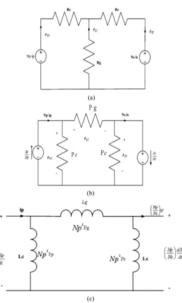
; . Fig. 9(a) shows the reluctance model for the proposed magnetic circuit. The electrical circuit model can be derived from the reluctance model by using the principle of duality, as shown in Fig. 9(b). The circuit of Fig. 9(c) results from scaling step with designated as the reference winding. The scaled permeances are then replaced by inductances. From the reluctance circuit shown in Fig. 9(a), the fluxes in the cores
can be derived in the form of reluctances and MMF sources, as follows:
(32)
(33)
where and represent the reluctances of the outer and center legs, and and are the total winding currents reflected to the primary and secondary of the transformer, respectively. According to Farady’s Law, and that the mutual inductance be-tween and is , and the coupling coefficient is k; the
re-Fig. 8. Characteristic curves for the proposed converter.
Fig. 9. (a) Reluctance model of proposed magnetic circuit. (b) Model (a) by using the principle of duality. (c) Model (b) of scaling step with Np designated as the reference winding.
Fig. 10. Flux distribution of the proposed structure by Ansoft simulation.
lationship between inductances and reluctances can be derived as follows:
(34)
(35)
(36)
(37)
Similarly, from the reluctance circuit shown in Fig. 9(c)
(38)
(39)
Since the reluctances from the magnetic material are much smaller than that of the air gap, the reluctance in the center leg is much larger than those of the outer legs , (34)–(37) can be simplified as follows:
(40)
(41)
(42) (43) Similarly, , (38)–(39) can be simplified as follows:
(44)
As can be seen from (35) to (37), in the proposed integrated magnetic structure, the coupling coefficient for the transformer is close to one. Two coupled windings still have a certain amount of leakage inductance. In practice, the reluctances from the mag-netic material influence the value of and . We now have an
Fig. 11. Equivalent electrical circuit for the proposed integrated magnetic circuits.
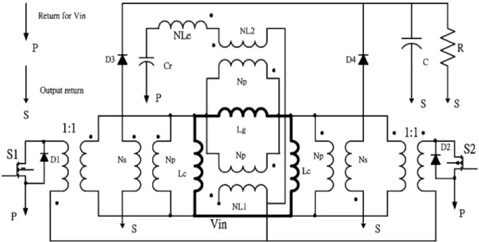
electrical model for the magnetic circuit as shown in Fig. 9(c). Substituting this model into the proposed converter of Fig. 6, re-sults in the equivalent SPC circuit shown in Fig. 11. Note that, in making this substitution, we have moved the inductance to the secondary side of the ideal transformer of turns ratio, : ( , or ). The two unit ideal transformers 1:1 are used for connecting the switch to the magnetic circuits for equivalent action.
D. Comparison of the Realization Variants
This section attempts to answer the question of how the appli-cation of a “zero” (or low)-ripple current technique for the pro-posed push–pull boost converter can be judged in comparison to a conventional passive filtering of the converter input current. Advantages of the converter structure according to Fig. 3(a) are as follows: i) only one magnetic core is required for the realiza-tion of the filter inductor and of the input inductor of the con-verter and ii) only a current ripple flows through inductor and not, as for conventional filtering, the full load current. This results in a relatively small rated power of the magnetic core and in low ohmic losses in the winding. Overall, a relatively small realization effort and a relatively high power density
are given.
On the other hand, the following disadvantages have to be mentioned: i) a defined, reproducible value of the coupling be-tween and can be guaranteed regarding manufacturing possibly only by an external balancing inductor lying in series to . The balancing of the winding turns ratios is connected with a relatively high manufacturing effort. ii) the magnetic integra-tion of and leads possibly to a higher parasitic coupling capacitance of the windings and to a less efficient suppression of high-frequency electromagnetic influences. The arrangement of and has to be realized.
In summary, the decision between different realization vari-ants of a “zero”-ripple boost converter has to be made, espe-cially on the basis of manufacturing points of view. This paper
Fig. 12. Measured MOSFET gate voltage (V g1, V g2) waveforms.
presents a novel single-stage push–pull boost converter with an improved integrated magnetics and better low-ripple input current.
IV. EXPERIMENTRESULT
The new push–pull boost converter was implemented, with the following specifications: nominal output power
150 W; output voltage 48 V; input voltage
110–120 V; switching frequency 150 KHz. The power stage consists of the following parameter: Switches and : power MOSFET’s IRF 740; Diodes and : HFA08TB60; Diodes and : HFA15TB40; Capacitor : 10 F; Couple
inductor 6.3 H; Extra inductor 1.3 H;
Core: TDK EI 35; 96 turns;
48 turns; 36 turns; 10 turns; Load R:
10 ; and Output capacitor C: 1000 F.
The switch conduction sequences of the proposed converter are shown in Fig. 12. It shows that the duty cycles greater than 50%. Thus, the proposed push–pull converter work in symmet-rical continuous conduction boost mode. Fig. 13 shows the input voltage waves and input current waveforms with and without
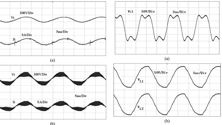
Fig. 13. Measured the input voltage (V t) and line current (It) waveform: (a) with input current shaper and (b) without input current shaper.
Fig. 14. Experiment results: the voltage across primary transformer (Vp).
input current shaper (ICS). The line current ( ) and line voltage ( ) of the proposed converter are shown in Fig. 13(a). It can be seen that the power factor is almost one. The ICS achieves a PFC and low ripple in this situation. And Fig. 13(b) shows the distortion input voltage waves for without ICS, where the ripple variation is very large. The voltage across primary transformer is shown in Fig. 14. The results are consistent with the typical waveforms in Fig. 3(b). Fig. 15(a) shows the voltage across ca-pacitor in the proposed topology. It can be seen that the voltage is the variation of . And the voltages across inductor , are shown in Fig. 15(b). It has the same wave and satis-fied the theoretical prediction. In order to demonstrate the theo-retical prediction, the proposed integrated magnetic converters with and without ICS and another discrete magnetic converter with ICS are implemented. The corresponding line-current har-monics are shown in Fig. 16 for three different cases. The odd order harmonics of input currents are expressed as a ratio
Fig. 15. Experiment results: (a) voltage across capacitorC1 and (b) the voltage across inductorL1, L2.
Fig. 16. Comparison of the corresponding line-current harmonics.
Fig. 17. Comparison of the efficiency.
of the fundamental current . The harmonic of the converter without ICS is the worst case. However, the harmonics of the proposed converter with integrated and discrete magnetic are approximately the same. It satisfies the better low-ripple condi-tion. Finally, the efficiency of the power stage of the three dif-ferent converters is shown in Fig. 17. The maximum value at full load is about 90%, and the converter without ICS filter is the worst case.
V. CONCLUSION
A novel simple single-stage push–pull ac–dc converter has been introduced. This converter can achieve small converter size and near zero-input current using coupled inductor techniques. The proposed circuit consists of a simple topology and con-trol strategy. It has several advantages such as lower switch and diode stress and lower stresses on capacitor . This makes the conduction and switching losses low and may result in a high efficiency. In this paper, a small capacitor is normally used as the input filter in the proposed topology, while a significant low-pass filter is used in the conventional boost converter. It has been proven that the proposed boost converter has the same steady-state properties as the conventional boost converter. Blending of the inductors and transformers of SPCs into single magnetic systems can be very advantageous, often resulting in converter designs of lower cost, weight, and size than their discrete mag-netic counterparts. Finally, conversion performance can also be improved and component stresses reduced, provided the inte-gration process is well thought out and executed properly.
REFERENCES
[1] C. Qiao and K. M. Smedley, “A topology survey of single-stage power factor corrector with a boost type input-current shaper,” IEEE Trans. Power Electron, vol. 16, no. 3, pp. 360–368, May 2001.
[2] O. García, J. A. Cobos, P. Alou, and J. Uceda, “A simple single-switch single-stage AC/DC Converter with fast output voltage regulation,” IEEE Trans. Power Electron, vol. 17, no. 2, pp. 163–171, Mar. 2002. [3] L. Huber and M. M. Jovanovic’, “Single-stage single-switch
input-current-shaping technique with fast-output-voltage regulation,” IEEE Trans. Power Electron, vol. 13, no. 3, pp. 476–486, May 1998. [4] Q. Zhao, F. C. Lee, and F. Tsai, “Voltage and current stress reduction
in single-stage power factor correction AC/DC converters with bulk capacitor voltage feedback,” IEEE Trans. Power Electron, vol. 17, no. 4, pp. 477–484, Jul. 2002.
[5] L. Huber, J. Zhang, M. M. Jovanovic’, and F. C. Lee, “Generalized topologies of single-stage input-current-shaping circuits,” IEEE Trans. Power Electron, vol. 16, no. 4, pp. 508–513, Jul. 2001.
[6] S. Hamada and M. Nakaoka, “A novel zero-voltage and zero-current switching PWM dc–dc converter with reduced conduction losses,” IEEE Trans. Power Electron, vol. 17, no. 3, pp. 413–419, May 2002.
[7] C. M. Duarte and I. Barbi, “An improved family of ZVS-PWM active-clamping DC-to-DC converters,” IEEE Trans. Power Electron, vol. 17, no. 1, pp. 684–691, Jan. 2002.
[8] J. Wang, W. G. Dunford, and K. Mauch, “Analysis of a ripple-free input-current boost converter with discontinuous conduction character-istics,” IEEE Trans. Power Electron, vol. 12, no. 4, pp. 684–694, Jul. 1997.
[9] J. Abu-Qahouq and I. Batarseh, “Unified steady-state analysis of soft-switching dc–dc converters,” IEEE Trans. Power Electron, vol. 17, no. 5, pp. 684–691, Sep. 2002.
[10] P. Xu, M. Ye, P. L. Wong, and F. C. Lee, “Design of 48 V voltage reg-ulator modules with a novel integrated magnetics,” IEEE Trans. Power Electron, vol. 17, no. 6, pp. 990–998, Nov. 2002.
[11] B. K. Bose, Power Electronics and AC Drives. Englewood Cliffs, NJ: Prentice-Hall, 1986.
[12] R. Severns and G. Bloom, Modern DC–DC Switchmode Power Con-verter Circuits. New York: Van Nostrand Reinhold, 1985.
Rong-Tai Chen was born in Kaohsiung, Taiwan,
R.O.C., on October 7, 1962. He received the M.S. degree in electrical engineering from National Tsing Hua University, Hsinchu, Taiwan, R.O.C., in 1993 and the Ph.D. degree in electrical engineering from National Taiwan University, Taipei, Taiwan, R.O.C., in 2005.
His current research interests include power elec-tronics, energy conversion, and intelligent control.
Yung-Yaw Chen received the B.S. degree in
elec-trical engineering from National Taiwan University, Taipei, Taiwan, R.O.C., in 1981, and the Ph.D. degree in electrical engineering and computer science from the University of California, Berkeley, in 1989.
He was with the Artificial Intelligence Branch, NASA, Ames, IA, in 1989. From 1993 to 1994, he was a Visiting Scholar at the University of California, Berkeley. He has been with the Depart-ment of Electrical Engineering, National Taiwan University, since 1989 and is currently a Professor and Vice Chairman. His research interests include intelligent fuzzy control systems, precision motion control, biomimetic systems, power electronics, and ultrasound hyperthermia.
Dr. Chen received nine NSC awards from 1990 to 2003 and the NTU Fu S-Nien Award in 2005.