252 IEEE ELECTRON DEVICE LETTERS, VOL. 27, NO. 4, APRIL 2006
Electroluminescence From the Ge Quantum
Dot MOS Tunneling Diodes
M. H. Liao, C.-Y. Yu, T.-H. Guo, C.-H. Lin, and C. W. Liu, Senior Member, IEEE
Abstract—A Ge quantum dot (QD) light-emitting diode (LED) is demonstrated using a MOS tunneling structure for the first time. The oxide film was grown by liquid phase deposition at 50 ◦C to reduce the thermal budget. The infrared emission of ∼ 1.5 µm was observed from Ge QD MOS LEDs, similar to the p-type–intrinsic–n-type structure reported previously. At the negative gate bias, the electrons in the Al gate electrode tunnel to the Ge QD through the ultrathin oxide and recombine radiatively with holes to emit the ∼ 1.5-µm infrared. The electrons also recombine with holes in the Si cap, and the band edge emission from Si is also observed.
Index Terms—Ge quantum dot (QD) light-emitting diodes (LEDs), MOS tunneling diode.
I. INTRODUCTION
I
T IS a long-sought goal to integrate ultralarge-scale inte-grated (ULSI) circuits with electrooptics to possibly over-come the speed limitation of electrical interconnects and to add extra functionalities on Si chip. Light-emitting diodes (LEDs) and detectors are essential devices to achieve this goal. The Si MOS LED has been demonstrated [1] to emit the 1.1-µm infrared at the Si band edge. The addition of Ge quantum dot (QD) into Si can tune the optical characteristic to longer wavelength, and the Ge QD MOS detector [2], [3] was reported to detect 1.3- and 1.5-µm infrared signals. The ∼ 1.5-µm infrared light emission was also observed in a previous study of electroluminescence (EL) from the Ge QD p-type–intrinsic– n-type (p-i-n) diodes [4]. However, the p-i-n structure is not fully compatible with the ULSI process. The building device in ULSI is the MOS structure. In this letter, we report that the Ge QD MOS tunneling diode can emit both the∼ 1.5-µm infrared from the Ge QD and the∼ 1.1-µm infrared from Si. The MOS tunneling diode reported here has the same structure used in the ULSI circuits, whereas the oxide is thin enough to have significant tunneling current from the metal to theManuscript received December 2, 2005; revised January 16, 2006. This work was supported by the National Science Council of Taiwan, R.O.C. under Contracts 93-2215-E-002-003, 93-2215-E-002-017, 94-2215-E-002-040, and 94-2215-E-002-041, and the Asian Office of Aerospace Research and Development (AOARD), U.S. Airforce. The review of this letter was arranged by Editor P. Yu.
M. H. Liao and T.-H. Guo are with the Department of Electrical Engineering and the Graduate Institute of Electro-Optical Engineering, National Taiwan University, Taipei 106, Taiwan, R.O.C.
C.-Y. Yu and C.-H. Lin are with the Department of Electrical Engineering and the Graduate Institute of Electronics Engineering, National Taiwan Univer-sity, Taipei 106, Taiwan, R.O.C. (e-mail: [email protected]).
C. W. Liu is with the Department of Electrical Engineering and the Graduate Institute of Electro-Optical Engineering and the Department of Electrical Engineering and the Graduate Institute of Electronics Engineering, National Taiwan University, Taipei 106, Taiwan, R.O.C.
Digital Object Identifier 10.1109/LED.2006.870416
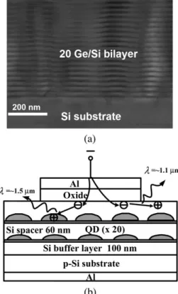
Fig. 1. (a) Cross-sectional TEM micrograph of the self-assembled Ge QD structure. (b) Schematic diagram of the Ge QD MOS LED device structure.
substrate. The fabrication for MOS LED does not need the n-type doping in the ultrahigh-vacuum chemical vapor depo-sition (UHV/CVD).
II. DEVICEFABRICATION
The Si/Ge QDs are prepared by UHV/CVD on p-type Si (001) substrates with resistivities in the range of 15–25 Ω· cm. After an Si buffer layer of 100 nm was grown, 20 periods of Ge QD structure with base and height of ∼ 120 and
∼ 7 nm, respectively, were grown at a temperature of 600◦C
under the Stranski–Krastanov (SK) growth mode [5] as shown in Fig. 1(a). The Ge layers are separated by 60-nm Si spacer layers. The Ge dot fabricated by the SK growth mode can lead to an increase of the luminescence efficiency because of the localization of excitons in the dots [6] and the increase of hole concentration in the dots. The area density of Ge islands is about 4× 109cm−2. A 3-nm (nominal thickness) Si cap was deposited above the top layer of the self-assembled Ge layer as a cap layer for the subsequent deposition of liquid phase deposition (LPD) oxide. The undoped Si/Ge layers has a background hole concentration of ∼ 1 × 1016 cm−3. Al is
0741-3106/$20.00 © 2006 IEEE
LIAO et al.: ELECTROLUMINESCENCE FROM Ge QUANTUM DOT MOS TUNNELING DIODES 253
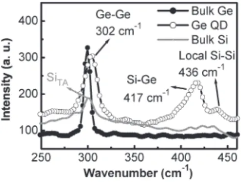
Fig. 2. Raman spectra of bulk Si, bulk Ge, and Ge QD. Ge/Ge, Si/Ge, and local Si/Si optical modes can be found at around 302, 417, and 436 cm−1, respectively.
used for the gate electrode and the back contact. Fig. 1(b) shows the device structure. To avoid material degradation such as strain relaxation and Ge out diffusion, the low-temperature oxide (LPD oxide) is used to reduce the thermal budget of the Si/Ge device process [3]. The tunneling current of electrons at the negative bias can cause electron–hole recombination at the oxide/Si interface and in the Ge QDs to emit ∼ 1.1- and
∼ 1.5-µm infrared, respectively. The momentum conservation
required by the indirect band gap can be achieved by Si/oxide roughness scattering, localized holes, and phonons scattering. Details were given in [7] and [8].
III. RESULTS ANDDISCUSSION
Fig. 2 shows Raman spectra excited by the 514-nm Ar laser for the Ge QD, bulk Ge, and bulk Si. In addition to the strong Si substrate signal at 520 cm−1, Ge-Ge, Si-Ge, and local Si-Si vibrational peaks were also observed at ∼ 302, ∼ 417, and
∼ 436 cm−1, respectively. The appearance of the Si-Ge and
the local Si-Si vibrational peaks implies the formation of Si-Ge alloy in the wetting layers [9]. On the other hand, the Ge-Ge peak is most possibly contributed by the islands [9]. As compared with the bulk Ge, the Raman shift of the Ge/Ge phonon frequency of the Ge QD with respect to the bulk Ge peak can be determined (∼ 2 cm−1). The possible factors responsible for this frequency shift are the alloying of the Ge QDs with Si spacers [10], the phonon confinement effect in the QDs, and the effects of compressive strain [11]. The first two factors reduce the phonon frequency, but the last mechanism increases the phonon frequency. Energy dispersion spectrometry shows the Ge dots transform into Si0.46Ge0.54 dots due to Si/Ge interdiffusion at the growth temperature of 600◦C.
Fig. 3 shows the photoluminescence (PL) spectra at different temperatures from the Ge QD before the fabrication of the MOS LED device at a pump power of 60 W/cm2. There are two PL peaks located at ∼ 1.1 and ∼ 0.85 eV. These two peaks are most likely from the optical transitions related to the Si substrate and the Ge QD [12]. Fig. 4 shows the EL spectra at different temperatures from the Ge QD MOS LED samples with a device size of 4× 10⁻⁴ cm2. The drive current is 100 mA at a gate voltage of −8 V. Device temperatures of
∼ 340, ∼ 250, ∼ 160, and ∼ 110 K are obtained from the
fitting of the EL line shapes from the Si signal with the
Fig. 3. PL spectra of the Ge QD at different temperatures. The infrared emission of∼ 1.1- and ∼ 1.5 µm was observed from the transition of Si and the Ge QD.
Fig. 4. EL spectra of the Ge QD MOS LED at different temperatures. The inset shows the energy band diagram of the Ge QD MOS LED at the accumulation bias. The EL spectra of the Ge QD p-i-n diode are also shown for reference.
electron–hole–plasma recombination model [1], [7], whereas the temperatures of the cold finger in the EL measurement are 300, 200, 100, and 10 K, respectively. The temperature differ-ence is due to the device heating. Because our Ge dot has a wide base (∼ 120 nm) and a short height (∼ 7 nm), the QD can be approximated by the quantum well in the electron–hole–plasma recombination model [13]. The band diagram of the Ge QD MOS LED at the accumulation condition is shown in the inset of Fig. 4. The traps in the LPD oxide and the small thickness (∼ 2 nm) allow the significant tunneling electrons to inject from the Al electrode into the semiconductor. At a negative bias, the electrons tunnel from the Al gate to the substrate. Meanwhile, the negative gate bias also attracts holes in the p-type semiconductor and QDs, and the tunneling electrons can recombine with holes at the oxide/Si interface and in the Ge QD to emit∼ 1.1- and ∼ 1.5-µm infrared, respectively [Fig. 1(b)]. The EL spectra of similar Ge QD p-i-n diode are also shown for reference. The infrared emission of ∼ 1.5 µm observed from the Ge QD MOS LED is similar to the p-i-n structure reported previously [4]. The external quantum efficiency for ∼ 1.5-µm light emission at∼ 110 K (∼ 340 K) from the Ge MOS LED was observed to be∼ 4 × 10⁻⁵(∼ 6 × 10⁻⁶), as compared to
∼ 9.5 × 10⁻⁵(∼ 1.2 × 10⁻⁵) for the Ge QD p-i-n diode. Note
that in our quantum efficiency measurement, we cannot collect all the light from the device, and the number presented here
254 IEEE ELECTRON DEVICE LETTERS, VOL. 27, NO. 4, APRIL 2006
is a lower bound of the true quantum efficiency. The efficiency is too low to have product applications, but the EL of the MOS structure is a good characterization tool for material quality and can be used in the in-line inspection in the industry. Note that the MOS structure is much simpler than the p-i-n structure to measure the EL spectra.
IV. CONCLUSION
The∼ 1.5-µm Ge QD MOS LED, which is fully compatible with the ULSI process, is reported for the first time. The origin of the emission is due to the radiative recombination between the electrons and the holes confined in the Ge QD. The electrons also recombined with the holes at the Si/oxide interface, and the band edge light emission from Si is also observed.
ACKNOWLEDGMENT
The authors would like to thank Prof. S. T. Chang and Prof. C.-T. Chia for helpful discussion.
REFERENCES
[1] C. W. Liu, M. H. Lee, M.-J. Chen, I. C. Lin, and C.-F. Lin, “Room-temperature electroluminescence from electron–hole plasmas in the metal oxide silicon tunneling diodes,” Appl. Phys. Lett., vol. 76, no. 12, pp. 1516–1518, Mar. 2000.
[2] B.-C. Hsu, S. T. Chang, T. C. Chen, P.-S. Kuo, P. S. Chen, Z. Pei, and C. W. Liu, “A high efficient 820 nm MOS Ge quantum dot photodetector,” IEEE Electron Device Lett., vol. 24, no. 5, pp. 318–320, May 2003.
[3] B.-C. Hsu, S. T. Chang, C.-R. Shie, C.-C. Lai, P. S. Chen, and C. W. Liu, “High efficient 820 nm MOS Ge quantum dot photodetectors for short-reach integrated optical receivers with 1300 and 1500 nm sensitivity,” in IEDM Tech. Dig., San Francisco, CA, 2002, pp. 91–94.
[4] Y. H. Peng, C.-H. Hsu, C. H. Kuan, C. W. Liu, P. S. Chen, M.-J. Tsai, and Y. W. Suen, “The evolution of electroluminescence in Ge quantum-dot diodes with the fold number,” Appl. Phys. Lett., vol. 85, no. 25, pp. 6107–6109, Dec. 2004.
[5] T. I. Kamins, D. A. A. Ohlberg, R. S. Williams, W. Zhang, and S. Y. Chou, “Positioning of self-assembled, single-crystal, germanium islands by silicon nanoimprinting,” Appl. Phys. Lett., vol. 74, no. 12, pp. 1773–1775, Mar. 1999.
[6] R. Apetz, L. Vescan, A. Hartman, C. Dieker, and H. Luth, “Photolumines-cence and electrolumines“Photolumines-cence of SiGe dots fabricated by island growth,” Appl. Phys. Lett., vol. 66, no. 4, pp. 445–447, Jan. 1995.
[7] C. W. Liu, M.-J. Chen, I. C. Lin, M. H. Lee, and C.-F. Lin, “Tempera-ture dependence of the electron–hole–plasma electroluminescence from metal–oxide–silicon tunneling diodes,” Appl. Phys. Lett., vol. 77, no. 8, pp. 1111–1113, Aug. 2000.
[8] C. W. Liu, M. H. Lee, M.-J. Chen, C.-F. Lin, and M. Y. Chern, “Roughness-enhanced electroluminescence from metal oxide silicon tunneling diodes,” IEEE Electron Device Lett., vol. 21, no. 12, pp. 601–603, Dec. 2000.
[9] J. L. Liu, Y. S. Tang, K. L. Wang, T. Radetic, and R. Gronsky, “Raman scattering from a self-organized Ge dot superlattice,” Appl. Phys. Lett., vol. 74, no. 13, pp. 1863–1865, Mar. 1999.
[10] W. J. Brya, “Raman scattering in Ge-Si alloys,” Solid State Commun., vol. 12, no. 4, pp. 253–257, Feb. 1973.
[11] F. Cerdeira, A. Pinczuk, J. C. Bean, B. Batlogg, and B. A. Wilson, “Raman scattering from GexSi1−x/Si strained-layer superlattices,” Appl. Phys. Lett., vol. 45, no. 10, pp. 1138–1140, Nov. 1984.
[12] L. P. Rokhinson, D. C. Tsui, J. L. Benton, and Y.-H. Xie, “Infrared and photoluminescence spectroscopy of p-doped self-assembled Ge dots on Si,” Appl. Phys. Lett., vol. 75, no. 16, pp. 2413–2415, Oct. 1999. [13] K. Eberl, O. G. Schmidt, O. Kienzle, and F. Ernst, “Preparation and optical
properties of Ge and C-induced Ge quantum dots on Si,” Thin Solid Films, vol. 373, no. 1–2, pp. 164–169, Sep. 2000.