新穎製程及新穎結構的複晶矽薄膜電晶體之可靠度研究
73
0
0
全文
(2) 新穎結構及新穎製程的複晶矽薄膜電晶體之可靠 度研究分析 研究生:馮立偉. 指導教授:張俊彥 博士. 國立交通大學 電子工程學系電子研究所. 摘要 本論文主要分為兩大部分 一、新穎抗衰退複晶矽薄膜電晶體元件之製作 二、新穎高性能複晶矽薄膜電晶體元件結構之改良. 在第一部份,我們提出了將氟離子藉由沈積間隙壁的過程中一同參雜其中,即 沈積氟矽玻璃來當間隙壁(Spacer)的輕量參雜結構(Light Doped Drain)薄膜複晶矽結 構,來探討此元件與一般 LDD 結構的可靠度分析。發現此新結構具除了有較少的 扭曲效應(Kink effect)外,在外加裂化時有較好的抗臨界電壓、驅動電流以及傳導電 導的劣化能力,主要是因為複晶矽介面與含氟的間隙壁之間而外產生較強的矽氟鍵 鍵結,不但修補掉複晶矽表面的懸浮鍵,而減少缺陷數目外,還因為矽氟鍵的鍵能 較一般矽氫鍵鍵能強兩倍,更能抵抗電流離子化的撞擊而更穩定。 I.
(3) 另一部份,我們提出了多重奈米通道結構的薄膜電晶體,發現其本身的電性效 能,在電流開關比(on/off ratio)、汲極引致通道能障底落(Drain Induce Barrier Lowing)、 和次臨界電導斜率(subthreshold slope)方面,較單條通道但卻具有近乎等效通道寬度 的電晶體而言要好。 此外,在外加直流與交流的劣化條件下,其也在臨界電壓、驅動電流以及傳導 電導方面有著優越的表現。其原因可能是由於多重通道結構具有優越的三面閘極 (tri-gate)控制能力,而能減低橫向電場所導致降低通道間的位障能而使得汲極電流 上升而造成更嚴重的劣化;也可能因為由於多條通道會使得電流分流,而減低自我 加熱效應(Self-Heating Effect),此外也可能因為本身結構所鈍化曝出的表面積較多及 移動率低,而降低表面缺陷和電子加速能量而使得抗劣化效果好。. II.
(4) Reliability Study of Novel Process and Novel Structure in Poly-Silicon Thin-Film Transistors. Student: Li-Wei Feng. Advisor: Dr. Chun-Yen Chang. Department of Electronics Engineering & Institute of Electronics National Chiao Tung University National Chiao Tung University Hsinchu, Taiwan, R.O.C.. Abstract. This thesis can be divided into two major parts: (1) Reliability study of novel fluorinated spacers process Poly-Si TFTs (2) Reliability study of novel multiple nanowire channels structure Poly-Si TFTs In the first part, high reliability polycrystalline silicon thin-film transistors (poly-Si TFTs) with lightly-doped drain (LDD) structure were obtained by using a self-aligned fluorinated silica glass (FSG) spacer technique. The output characteristics of FSG spacer show the superior immunity to kink effect. It is also found that the degradations in Vth shifting, drain current and trans-conductance of FSG spacer after DC stress are improved. III.
(5) This is attributed to the passivation of fluorine ions reduces the trap states in the LDD region. Additionally, the stronger Si-F bonds also reduce the bonds broken by impact ionization. In the second part, the experiment results reveal that the novel multiple nanowire structure poly-Si TFTs has a lower DIBL, a lower SS and a higher on/off ratio than the single-channel TFT. In static and dynamic stress reliability experiments, the multiple nanowire poly-Si TFTs reduces the degradation of Vth, SS, Ion, and On/OFF ratio, compared to single-channel TFT. These high reliability results of multiple nanowire poly-Si TFTs can be explained by its robust tri-gate control and its superior channel NH3 passivation for reducing the poly-Si grain boundary defects.. IV.
(6) 誌謝 終於,兩年的碩士班研究生活,以此論文之告成,即將告一段落。在這兩年裡 首先要感謝張俊彥老師與張鼎張老師的細心指導實驗研究與論文上給予充分詳實的 指導與鼓勵,此外也讓我學到很多寶貴的知識和學問,也學到處理事情的態度和方 法,使我有想法與啟發。感謝我的家人,尤其是我的父親與母親,能在我求學的階 段提供給我莫大的幫助與鼓勵,讓我能無後顧之憂地順利完成學業。. 此外也很感學實驗室各學長吳師道、陳經緯、楊中熹、彭辭修、王丁勇、羅文 政、陳漢譽、吳永俊、涂峻豪、蔡宗鳴、顏碩廷、陳致宏、楊富明、黃聖懿、胡佳 欣、胡心卉、陳怡誠、吳興華、張保安、張家榮、郭柏儀、楊政桓、吳元均、黃子 軒、陳稚軒、林泩宏等的帶領與指教,特別感謝吳永俊學長等在我的論文寫作與口 試報告等方面的教導,以及電腦軟體使用與量測分析的傳授;及涂俊豪學長、吳興 華學長、張保安學長等在儀器與實驗方面的傳授教導;另外也感謝實驗上的同伴鄭 兆欽、馮立偉、楊哲育、楊道彥、何武凌、張智超、翁崎峰、許雁雅、等在實驗上 的幫忙。感謝以上的所有人,讓我能順利的在這碩士期間完成實驗與論文。 其次感謝國家奈米元件實驗室的員工巫振榮、蔣秋芬、楊君慧、楊明瑞、洪鵬 飛…等,在實驗中給予我種種的支援,讓我得以順利完成我的實驗。女朋友在背後 默默的支持,讓我得以完成我的學業。再次衷心的感謝上述諸位由於各位的幫忙此 論文得以如期完成。. V.
(7) Contents Chinese Abstract. I. English Abstract. III. Acknowledgement (Chinese). V. Contents. VI. Figure Captions. VIII. Table Captions. XI. Chapter 1. Introduction. 1. 1-1. Overview of polysilicon thin-film transistors technology 1 1-2. Motivation. 4. 1-3. Thesis outline. 6. Chapter 2. Poly-Si TFT conduction mechanism and reliability after static and dynamic stress. 8. 2-1. TFT transportation mechanism. 8. 2-2. Method of Device Parameter Extraction. 11. 2-2-1. Determination of the threshold voltage. 12. 2-2-2. Determination of the subthreshold swing. 12. 2-2-3. Determination of On/Off Current Ratio. 12. 2-2-4. Determination of the field-effect mobility. 13. 2-3. Stress mechanism. 14. 2-3-1. Static Hot-Carrier Stress. 14. 2-3-2. Dynamic Hot-carrier Stress. 16. Chapter 3.. Device structure and Fabrication. 19. Part I. Poly-Si TFT with Self-aligned Fluorinated Silica Glass (FSG) Spacers 3-1. Fluorinated Silica Glass (FSG) Spacers Device Structure 19 3-2. FSG Spacers Device Fabrication Process 19 Part II. Novel Multiple Nanowire Channels Poly-Si Thin-Film Transistors 3-3. Multiple Nanowire Channels Device Structure 22 3-4. Multiple Channels Device Fabrication Process 23 Chapter 4. Experiment results and discussion 30 Part I. Poly-Si TFT with Self-aligned Fluorinated Silica Glass (FSG) Spacers VI.
(8) 4-1. Performance of Fluorinated and TEOS Spacers Poly-Si TFTs and width effect 4-2. Reliability after DC stress of Fluorinated and TEOS Spacers Poly-Si TFTs Part II. Novel Multiple Nanowire Channels Poly-Si TFTs 4-3. Performance of Novel Multiple Nanowire Channels Poly-Si TFTs 4-4. Reliability after DC and AC stress of Novel Multiple Nanowire Channels Poly-Si TFTs Chapter 5. Conclusion. 36 55. References. 57. VII. 30 31. 34.
(9) Figure captions. Chapter 2 Fig. 2-1 Sketch of the band diagram of the polycrystalline silicon films Fig. 2-2 A schematic MOSFET cross section, showing the axes of coordinates and the bias voltages at the four terminals for the drain-current model. Fig. 2-3 Kink effect is due to the holes injected and stored in a floating body to cause the reduction of the threshold voltage and a parasitic bipolar element is resulting in positive-feedback effect to enhance the generation of the hot-carriers.. Chapter 3 Fig. 3-1 The cross section view of the Fluorinated Silica Glass (FSG) Spacers Device Structure. Fig. 3-2. (a) Schematic diagram of M10 poly-Si TFT. (b) Cross-section view of Fig. 1a AA’ direction, as a conventional top-gate LDD MOSFET structure. (c) One of channel cross-section view of Fig. 1a BB’ direction, as a tri-gate structure. Active layer, gate oxide, and poly-gate thickness are 50 nm, 26 nm and 150 nm, respectively t.. Fig. 3-3. Simulation results of potential contour plots and electrical field lines of (a) single-top-gate TFT (b) tri-gate TFT with L = 0.5 um, gate oxide = 26 nm, channel thickness = 50 nm at Vg = 0 V, Vd = 2 V.. Fig. 3-4. (a) Scanning electron microscopy (SEM) photography of active pattern with the source, the drain and multiple nano-wire channels of M10 TFT. (b) Magnified area of multiple nano-wire channels. The each nano-wire width is. VIII.
(10) 67 nm. (c) Transmission electron microscopy (TEM) photography of poly-Si grains by solid phase crystallization. The average poly-Si grain size is about 30 nm.. Chapter 4 Fig. 4-1 FTIR Spectra of FSG film and TEOS film between 2000cm-1 and 400 cm-1. Fig. 4-2(a) Comparsion of Id-Vg characteristics of FSG spacer TFT and TEOS spacer TFT for Vd=0.1 V (W/L=10um/5um). Fig. 4-2(b) Comparsion of output characteristics for FSG spacer and TEOS spacer TFT, W/L=10um/5um, VG-Vth= 0,1,2,3,4 V. Fig. 4-3(a) The degradation of drain current and trans-conductance by static stress in TEOS spacer structure. Fig. 4-3(b) The degradation of drain current and trans-conductance by static stress in SiOF spacer structure Fig. 4-4 Comparsion of ∆Gm/Gm characteristics of SiOF spacer TFT and TEOS spacer TFT for Vd=0.1V (W/L=10um/3um). Fig. 4-5 Comparsion of ∆Ion characteristics of SiOF spacer TFT and TEOS spacer TFT for Vd=5V (W/L=10um/3um). Fig. 4-6 Comparsion of ∆Vth characteristics of FSG spacer TFT and TEOS spacer TFT for Vd=0.1V (W/L=10um/3um). Fig. 4-7 Comparison of ∆SS characteristics of SiOF spacer TFT and TEOS spacer TFT for Vd=0.1V (W/L=10um/3um). Fig. 4-8 Comparison of Id-Vg transfer characteristics of multiple nano-wire channels (W/L = 67nm×10/0.5um) and single-channel (W/L = 1um/0.5um) polysilicon IX.
(11) TFTs. Fig. 4-9 Comparison of Id-Vd output characteristics of multiple nano-wire channels (W/L = 67nm×10/0.5um) and single-channel (W/L = 1um/0.5um) polysilicon TFTs. Fig. 4-10 Effective trap state density of multiple nano-wire channels (W/L = 67nm× 10/0.5um) and single-channel (W/L = 1um/0.5um) polysilicon TFTs. Fig. 4-11 The AC stress waveform of the pulse train. Fig. 4-12(a) Typical M10 poly-Si TFT Id-Vg curves before and after DC hot carrier stress at 10000 second. Fig. 4-12(b) Typical S1 poly-Si TFT Id-Vg curves before and after DC hot carrier stress at 10000 second. Fig. 4-13 Transconductance degradation of S1 and M10 TFT as a function of the stress time with different frequencies (DC, f = 1K Hz, and f = 1M Hz). Fig. 4-14 Teshold voltage of S1 and M10 TFT as a function of the stress time with different frequencies. Fig. 4-15 Subthreshold swing variation of S1 and M10 TFT as a function of the stress time with different frequencies. Fig. 4-16 ON current (ION) variation of S1 and M10 TFT as a function of the stress time with different frequencies. Fig. 4-17 ON/OFF ratio of S1 and M10 TFT as a function of the stress time with different frequencies. Fig. 4-18 Gm degradation of S1 and M10 TFT as a function of the stress time with different rising time (Tr) and falling time (Tf) under the frequency of 1 KHz. Fig. 4-19 Dependence of emission intensity on (a) pulse rise time and (b) pulse fall time. Emission intensity is independent of the pulse rise time. However,. X.
(12) we have found that it strongly depends on the fall time. Fig. 4-20 Vth variation of S1 and M10 TFT as a function of the stress time with different rising time (Tr) and falling time (Tf) under the frequency of 1 KHz. Fig. 4-21 ON current (Ion) degradation of S1 and M10 TFT as a function of the stress time with different rising time (Tr) and falling time (Tf) under the frequency. Fig. 4-22 Gm degradation of S1 and M10 TFT as a function of the stress time with different subtract temperature with 250C, and 750C under the same frequency of 1 KHz. Fig. 4-23 Vth variation of S1 and M10 TFT as a function of the stress time with 250C, and 750C under the same frequency of 1 KHz. Fig. 4-24 ON current (Ion) degradation of S1 and M10 TFT as a function of the stress time with 250C, and 750C under the same frequency of 1 KHz.. Table captions Table 1. Variation of experimental electronic parameters and corresponding possible degradation mechanics.. Table II Device parameters of single-channel TFTs with L/W = 0.5um/1um, and multiple nano-wire channels TFTs with L/W = 0.5um/67nm×10. All parameters were extracted at Vd = 2V, except for the field-effect mobilities which were extracted at Vd = 0.05V.. XI.
(13) Chapter 1 Introduction. 1-1. Overview of polysilicon thin-film transistors technology The interest in polycrystalline silicon thin-film transistors (poly-Si TFTs) has drastically increased in recent years because of their widely applications on active matrix liquid crystal displays (AMLCDs)[1], and organic light-emitting displays (OLEDs)[2]. Except displays application, poly-Si TFTs also have been applied into some memory devices such as dynamic random access memories (DRAMs)[3], static random access memories (SRAMs)[4], electrical programming read only memories (EPROM)[5], electrical erasable programming read only memories (EEPROMs)[6], linear image sensor[7], thermal printer heads[8], photo-detector amplifier[9], scanner[10], neutral networks[10]. Recently, some superior performances of poly-Si TFTs also have been reported by scaling down device dimension or utilizing novel crystallization technologies to enhance poly-Si film quality [11.12]. This provides the chance for applying poly-Si TFTs into three-dimension (3-D) integrated circuit fabrication. Of course, the application in AMLCDs is the primary trend, which leads to rapid development of poly-Si TFT technology. Currently, the main application of poly-Si TFT processed at low temperature. 1.
(14) (below 6000C) is the AMLCDs and AMOLED. The electron mobility of a poly-Si TFTs ranged from few tens to several hundred cm2/Vs which are several orders of magnitude higher than in amorphous-Si (a-Si) TFT. That is enough to be used as peripheral-driving circuits including n- and p- channel devices. The fabrication of peripheral circuit can be integrated into the structure, i.e., peripheral circuits and switch pixel elements can be on the same glass substrate, and therefore, it reduces the size of the total panel[13]. In addition, for the dimension of the poly-Si TFTs can be made smaller compared to that of amorphous Si TFTs for high density, high resolution AMLCDs, and the aperture ratio in TFT array can be significantly improved by using poly-Si TFTs as pixel switching elements[14]. This is because the device channel width can be scaled down while achieving the same pixel driving requirements as in a-Si TFT AMLCDs. However, reliability of ploy-Si TFT is one of the main constraints toward this direction. In comparison with single-crystalline silicon, granular structure of poly-Si is rich in grain boundary defects arising from lattice discontinuities between different oriented grains as well as intra-grain defects. Moreover, a low process temperature, i.e. less than 600 0C, also produces numerous defects at the poly-Si\SiO2 interface and poly-silicon boundaries. Under the operation of high drain voltage and a relatively high gate voltage (hot-carrier condition), the defects acting as trapping centers lead to. 2.
(15) hot-carrier injection that generates trap states to trap carriers. Carriers trapped by these low energy traps can no longer contribute to conduction, which results in the formation of local depletion region and potential barriers in these grain boundaries. Thus, those trap states are strongly influenced the performance of poly-TFTs and causes severe device degradation. Large leakage current inducing the charge holding issue of AMLCDs is resulted from carrier generation from the poly-Si grain boundary defects. Also, the typical characteristics such as threshold voltage (Vth), subthreshold swing (SS), ON current (Ion), field effect mobility (µeff) and transconductance (Gm) of TFTs are inferior to those of devices fabricated on single crystal silicon film. The (Gm)max degradation and Vth variation during stress application which results in improper operation and circuit failure is of great importance for circuit designers in order to integrate TFTs in flat-panel displays or VLSI circuits. There are several approaches toward these obstructions. The main propose is modifying or eliminating these grain boundary traps associated with dangling bonds. One is the enlargement of poly-Si grains, which reduces the total length of the poly-Si grain boundaries in the channel area. However, this approach enhances the variation of TFT performance.. Another approach is the passivation of the grain boundary. traps. Generally, hydrogenation has been utilized for the passivation, but the hydrogenated TFT has poor immunity against the negative bias temperature stress.. 3.
(16) In this thesis, we apply novel process and novel structure to improve the poly-Si reliability. In the novel process of poly-Si TFT, a self-aligned fluorinated silica glass (FSG) spacers with Si-F bonds formation near the interface of source and drain is used due to its stronger dissociation energy of Si-F bonds. In the novel structure TFT, the multiple nano-wire channels with surrounding gate electrode is used due to the superior gate controllability. Two kinds of TFTs are introduced to achieve high reliability under static and/or dynamic stress.. 1-2. Motivation Although poly-Si TFTs have many superior advantages, the presence of a large number of grain boundaries in poly-Si TFTs contributes a large density of defects which cause the localized states in the energy gap and degrade performance. So the reliability issue is one of the most constraints toward the applications. There are many investigations about the improvement of the poly-Si TFTs reliability. It is reported about the reliability improvement in poly-Si TFTs by fluorine implantation. But it needs an extra implantation, which may cause the implantation damage in the active layer and shifts the threshold voltage. It is known that one of the degradation is caused by the energetic electrons generated by impact ionization near the drain. So we introduce the fluorinated spacer technique to generate the higher dissociation Si-F bonds adjust to the interface of the drain which is the largest lateral. 4.
(17) electric field region for light doped drain structure. This method needs not additional process step and also can achieve the improvement of reliability. In the structure aspect, according to CMOS technology, several high performance surrounding gate structures in silicon on insulator (SOI) MOSEFT, such that double-gate, gate-all-around, tri-gate[16], and FinFET[17], have been reported that they have superior gate control over channel than conventional single-gate MOSFET to reduce the non-ideal effects. Thus we employed multiple channels and LDD structure to investigate the reliability on the surrounding gate controllability. For devices with smaller dimension, the number of grain boundaries decreases since there are fewer grains within the channel region. Because the drain voltage drops mainly on the depletion regions located at grain boundaries, fewer grain boundaries represent larger voltage drop on each depletion region under the same drain voltage. Therefore, a large electric field will exist in small dimension TFTs to induce impact ionization effect. If the electric field exceeds 105 V/cm, the impact ionization effect will occur and the drain current will increase dramatically. To overcome this inherent disadvantage of small dimension of TFT, we apply the lightly-doped drain (LDD) structure to reduce the lateral electrical field in channel.. 5.
(18) 1-3. Thesis Outline Chapter 1. Introduction 1-1. Overview of polysilicon thin-film transistors technology 1-2. Motivation 1-3. Thesis outline Chapter 2. Poly-Si TFT conduction mechanism and reliability after static and dynamic stress 2-1. TFT transportation mechanism 2-2. Methods of device parameter extraction 2-2-1. Determination of the threshold voltage 2-2-2. Determination of the subthreshold slope 2-2-3. Determination of On/Off Current Ratio 2-2-4. Determination of the field-effect mobility 2-3. Stress mechanism 2-3-1. Static Hot-Carrier Stress 2-3-2. Dynamic Hot-carrier Stress Chapter 3 Device structure and Fabrication 3-1. Fluorinated Silica Glass (FSG) Spacers Device Structure 3-2. FSG Spacers Device Fabrication Process. 6.
(19) 3-3. Multiple Nanowire Channels Device Structure 3-4. Multiple Channels Device Fabrication Process Chapter 4 Experiment results and discussion 4-1. Performance of Fluorinated and TEOS Spacers Poly-Si TFTs 4-2. Reliability after DC stress of Fluorinated and TEOS Spacers Poly-Si TFTs 4-3. Performance of Novel Multiple Nanowire Channels Poly-Si TFTs 4-4. Reliability after DC and AC stress of Novel Multiple Nanowire Channels Poly-Si TFTs Chapter 5 Conclusion References. 7.
(20) Chapter 2 Poly-Si TFT conduction mechanism and reliability after static and dynamic stress. 2-1. TFT transportation mechanism As mentioned in section 1-1 and 1-2, the device characteristics of poly-Si TFTs are strongly influenced by the grain structure in poly-Si film. Even though the inversion channel region is also induced by the gate voltage as in MOSFETs, the existence of grain structure in channel layer bring large differences in carrier transport phenomenon. Many researches studying the electrical properties and the carrier transport in poly-Si TFTs have been reported. A simple grain boundary-trapping model has been described by many authors in details. In this model, it is assumed that the poly-Si material is composed of a linear chain of identical crystallite having a grain size Lg and the grain boundary trap density Nt. The charge trapped at grain boundaries is compensated by oppositely charged depletion regions surrounding the grain boundaries. From Poisson’s equation, the charge in the depletion regions causes curvature in the energy bands, leading to potential barriers that impede the movement of any remaining free carriers from one grain to another. When the dopant/carrier density n is small, the poly-Si grains will be fully depleted. The width of the grain. 8.
(21) boundary depletion region xd extends to be Lg/2 on each side of the boundary, and the barrier height VB can be expressed as qn 2 qnL g VB = xd = 2ε s 8ε s. 2. (1-1). As the dopant/carrier concentration is increased, more carriers are trapped at the grain boundary. The curvature of the energy band and the height of potential barrier increase, making carrier transport form one grain to another more difficult. When the dopant/carrier density increases to exceed a critical value N* = Nt / Lg, the poly-Si grains turn to be partially depleted and excess free carriers start to spear inside the grain region. The depletion width and the barrier height can be expressed as xd =. Nt 2n. (1-2) 2. qn N t 2 qN t VB = ( ) = 2ε s 2n 8ε s n. (1-3). The depletion width and the barrier hight turn to decrease with increasing dopant/carrier density, leading to improved conductivity in carrier transport. The carrier transport in fully depleted poly-Si film can be described by the thermionic emission over the barrier. Its’ current density can be written as 23. J = qnvc exp[−. q (V B − V )] kT. (1-4). where n is the free-carrier density, vc is the collection velocity ( vc = kT / 2πm ∗ ), VB. is the barrier height without applied bias, and Vg is the applied bias across the grain. 9.
(22) boundary region. For small applied biases, the applied voltage divided approximately uniformly between the two sides of a grain boundary. Therefore, the barrier in the forward-bias direction decreases by an amount of Vg/2. In the reserve-bias direction, the barrier increases by the same amount. The current density in these two directions then can be expressed as J F = qnvc exp[−. q 1 (VB − Vg ] kT 2. (1-5). J R = qnvc exp[−. q 1 (VB + Vg )] kT 2. (1-6). the net current density is then given by J = 2qnvc exp(−. qV g qVB ) sinh( ) kT 2kT. (1-7). at low applied voltages, the voltage drop across a grain boundary is small compared to the thermal voltage kT/q, Eq. (1.7) then can be simplified as J = 2qnvc exp(−. 2 qV B qV g q nv cV g qV ) = [exp(− B )] kT 2kT kT kT. (1-8). the average conductivity σ = J / Ε = JLg / Vg and the effective mobility µeff = σ / qn then can be obtained. σ=. q 2 nvc Lg. µ eff =. kT qvc L g kT. exp(−. qVB ) kT. (1-9). exp(−. qVB qV ) ≡ µ 0 exp(− B ) kT kT. (1-10). where µ0 represents the carrier mobility inside grain regions. It is found that the conduction in poly-Si is an activated process with activation energy of approximately qVB, which depends on the dopant/carrier concentration and the grain boundary trap. 10.
(23) density. Applying gradual channel approximation to poly-Si TFTs, which assumes that the variation of the electric field in the y-direction (along the channel) is much less than the corresponding variation in the y-direction (perpendicular to the channel), as shown Fig. 2-2. The carrier density n per unit area (cm-2) induced by the gate voltage can be expressed as n=. Cox (VG − VTH − V( y ) ). (1.11). qtch. I D = ∫∫ J .dx.dz = ∫∫ nq µeff . W. tch. 0. 0. = ∫ µeff dz ∫ nqdx.. dVy dy. dv y dy. .dx.dz. (1.12). = W µeff .Cox (Vg − Vth − Vy ). dVy dy. where tch is the thickness of the inversion layer. Therefore, the drain current ID of poly-Si TFT then can be given by. ∫. L. 0. 1 I D dy = W µ ff Cox ⎡⎣(Vg − Vth ) VD − VD 2 ⎤⎦ 2. ID =. W 1 µ ff Cox ⎡⎣(Vg − Vth ) VD − VD 2 ⎤⎦ L 2. (1-13). Obviously, this I-V characteristic is very similar to that in MOSFETs, except that the mobility is modified.. 2-2. Methods of device parameter extraction In order to clarify the possible mechanisms, the device electrical parameters are important. The methods of typical parameters extraction such as threshold voltage. 11.
(24) (Vth), subthreshold slope (SS), drain current ON/OFF ratio, field-effect mobility (µFE) are defined as followed: 2-2-1. Determination of the threshold voltage. Many ways are used to determinate the Vth which is the most important parameter of semiconductor devices. In poly-Si TFTs, the method to determinate the threshold voltage is constant drain current method. The gate voltage at a specific drain current IN value is taken as the threshold voltage. This technique is adopted in most studies of TFTs. Typically, the threshold current IN = ID / (Weff / Leff ) is specified 100 nA for Vd in saturation region in this thesis. 2-2-2. Determination of the subthreshold slope. Subthreshold slope SS (V/dec.) is a typical parameter to describe the gate control toward channel. The SS should be independent of drain voltage and gate voltage. However, in reality, SS might increase with drain voltage due to short-channel effects such as charge sharing, avalanche multiplication, and punchthrough-like effect. The SS is also related to gate voltage due to undesirable factors such as serial resistance and interface state. In this experiment, the SS is defined as one-half of the gate voltage required to decrease the threshold current by two orders of magnitude (from 10-8A to 10-9A). 2-2-3. Determination of On/Off Current Ratio. 12.
(25) Drain On/Off current ratio is another important factor of TFTs. High On/Off ratio represents not only large turn-on current but also small off current (leakage current). It affects gray levels (the bright to dark state number) of TFT AMLCD directly. There are many methods to specify the on and off current. The practical one is to define the maximum current as on current and the minimum leakage current as off current while drain voltage is in saturation region. 2-2-4. Determination of the field-effect mobility. The field-effect mobility (µFE) is determined from the transconductance (gm) at low drain voltage (Vd = 0.1V). The transfer I-V characteristics of poly-Si TFT can be expressed as I D = µ FE C ox. W 1 2 [(VG − VTH )V D − VD ] L 2. (3-1). where Cox is the gate oxide capacitance per unit area, W is channel width, L is channel length, VTH is the threshold voltage. If VD is much smaller than VG-VTH ( i.e. VD << VG-VTH ) and VG > VTH, the drain current can be approximated as: I D = µ FE C ox. W (VG − VTH )VD L. (3-2). 13.
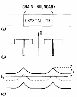
(26) The transconductance is defined as. gm =. ∂I D ∂VG. VD = const .. =. WC ox µ FE VD L. (3-3). Therefore, the field-effect mobility can be obtained by µ FE =. L gm C ox WV D. (3-4). 2-3. Stress mechanism 2-3-1 Static Hot-Carrier Stress It is reported that the ON-state stressing is the limiting instability condition in poly-TFTs[2-1] which is in contrast to hydrogenated amorphous silicon (a-Si:H) TFT’s, where the degrading rate depends only on the gate bias and is independent of drain bias[2-2]. During the operation of poly-TFTs with grain boundary defects and intra-grain defects in Poly-Si film and a large number of interface states at the SiO2/poly-Si interface, most of the applied voltage drops across the grain boundaries since they have much larger resistances than the grains. The lateral electric field in the grain boundaries will be much higher than in the grains, and at large drain voltages, impact ionization may occur. Then the generated hot-carriers will be injecting into the gate oxide and/or breaking the Si-H bonds and strained Si-O bonds[2-3]. Moreover, the poly-TFTs’ non-ideal effect, Kink effect, which is due to the holes injected and stored in a floating body to cause the reduction of the threshold voltage and a parasitic bipolar element is resulting in positive-feedback effect to enhance the generation of 14.
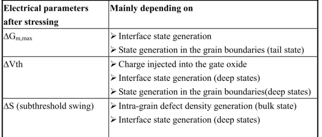
(27) the hot-carriers shown in fig.2-3[2-4]. This kink effect associated with float-body is especially dramatic for n-channel devices, because of the higher impact-ionization rate of electrons. Unlike to the fundamental MOSFETs theory, the poly-Si TFT electrical parameters such as threshold voltage (Vth), maximum transconductance (Gm,max), On current (Ion), and subthreshold slope (SS) could depend on grain, grain boundaries, and/or interface properties. The deep traps existing in grain boundaries have been demonstrated to affect mainly threshold voltage and much less Gm,max. On the other hand, tail states from grain regions in the interface and/or from grain boundaries mainly contribute to the decrease of (Gm)max [2-5][2-6]. The subthreshold slope depends mainly on intra-grain traps distributed uniformly inside the poly-Si film and also on the deep interface states [2-7]. Therefore, it is obvious that depending on the nature of state generation after stress, electrical parameters can provide useful information in order to clarify poly-Si TFTs degradation under hot carrier stress conditions. These points are summarized on the Table I. Self-heating effect is also another mechanism especially occurred in the wide-channel poly-Si TFTs that is because the temperature of poly-Si TFTs can reaches over 3500C during the operation in the high stress power(stress power = Vds × Id) condition to dissolute the weak Si-H bonds [2-8].. 15.
(28) 2-3-2 Dynamic Hot-carrier Stress Dynamic stress is closer to real operation condition than the static stress. It is reported that the reliability evaluation method proposed under the static stress conditions may not be suitable for the reliability evaluation under the dynamic stress [2-9].. The dynamic stress degrades the poly-Si TFT more seriously than the static. stress. The impact ionization generation hot electrons and hot holes near drain at ON state. However, as the device is changed from ON state to OFF state, the drain avalanche hot carrier (DAHC) will occur to cause serious degradation and generate more hot electrons and hot holes near drain [2-10].At the switching period, a transient current (I = C dV/dt) can be observed to damage the device [2-11]. According the pervious reports, the dynamic stress degradation mainly depend on the stress frequency (f), stress temperature, and falling time (Tf)[2-12].. 16.
(29) Fig. 2-1. Sketch of the band diagram of the polycrystalline silicon films. Vg z y. W. Vd. Gate. x. Gate oxide. Source N+. Drain. t. N+. L. 0. Fig. 2-2. A schematic MOSFET cross section, showing the axes of coordinates and the bias voltages at the four terminals for the drain-current model.. 17.
(30) Gate Impact ionization. electron injection. e-. e-. +. +. e-. eh+. Source h. h. e-. Drain. Hole accumulation/injection Fig. 2-3. Kink effect is due to the holes injected and stored in a floating body to cause the reduction of the threshold voltage and a parasitic bipolar element is resulting in positive-feedback effect to enhance the generation of the hot-carriers. Table 1 Variation of experimental electronic parameters and corresponding possible degradation mechanics. Electrical parameters after stressing. Mainly depending on. ∆Gm,max. ¾ Interface state generation ¾ State generation in the grain boundaries (tail state). ∆Vth. ¾ Charge injected into the gate oxide ¾ Interface state generation (deep states) ¾ State generation in the grain boundaries(deep states). ∆S (subthreshold swing). ¾ Intra-grain defect density generation (bulk state) ¾ Interface state generation (deep states). 18.
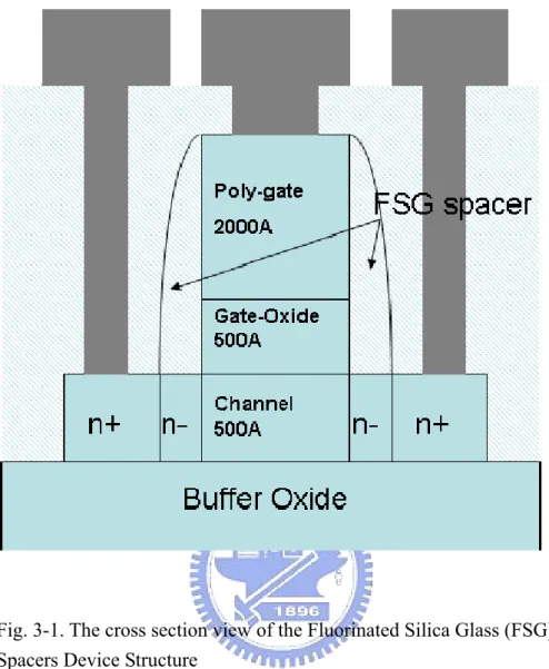
(31) Chapter 3 Device structure and Fabrication. In this thesis, the novel process TFT with self-aligned fluorinated silica glass (FSG) spacers mentioned and their fabrications are described in part I. The new structure TFT with multiple nanowire channels mentioned and their fabrications are described in part II.. Part I. Poly-Si TFT with Self-aligned Fluorinated Silica Glass (FSG) Spacers 3-1. Fluorinated Silica Glass (FSG) Spacers Device Structure We fabricate the conventional top-gate Light Doped Drain (LDD) polysilicon TFT structure incorporated with fluorinated silica glass (FSG) spacer and conventional TEOS silicon dioxide spacer. The schematic cross section view of devices is shown in Fig. 3-1. The devices used here have a gate width W=10 um and length L=3 um. In these devices, high reliability on FSG spacers of TFT can be observed.. 3-2. FSG Spacers Device Fabrication Process Step1. Substrate. 6-inch p-type single crystal silicon wafers with (100) orientation were used as the starting materials. After an RCA initial cleaning procedure. Si wafers were 19.
(32) coated with 550-nm-thick thermally grown SiO2 in steam oxygen ambient at 980°C. Step2. Active region formation. Uundoped 50nm-thick amorphous-Si layer were deposited by low-pressure chemical vapor deposition (LPCVD) on buried oxide by pyrolysis of silane (SiH4) at 550°C. The amorphous-Si films were recrystallized by solid phase crystallization (SPC) method at 600°C for 24 hrs in N2. The active islands (mask1), including source, drain and channel with different dimension, were patterned and transferred by reactive ion etching (RIE) (transformer couple plasma) using the mixture of Cl2 and HBr. Step3. Gate oxide formation. After defining the active region, the wafers were boiled in H2SO4 + H2O2 to ensure cleanliness of the wafers before deposition. A buffered HF dip was performed to remove the native oxide on the silicon surface. Soon, the gate insulator was deposited in a horizontal furnace using TEOS and O2 gases at 700°C. The thickness of the TEOS oxide thin film is 50nm. Step4. Gate electrode formation. After deposition of gate oxide, 200nm-thick undoped poly-Si films were deposited immediately on the gate oxide by LPCVD at 620°C. The poly-Si layers were patterned and transferred by RIE (transformer couple plasma) to define the gate electrode and to be the mask for self-aligned implantation. Step5. Self-aligned LDD N- implantation and annealing . After gate electrode formation, phosphorus ions at a dose of 5×1013 cm-2 and an energy of 17keV were implanted to form the light doped source/drain regions. Then all wafers were subjected to a rapid thermal anneal (RTA) at 820°C for 20.
(33) 20seconds for dopants activation. Step6. fluorine doped TEOS oxide spacer formation. After n- implantation and dilute HF dip to remove the native oxide, the wafer was loaded into a plasma enhanced chemical vapor deposition (PECVD) system using the mixture gases of CF4 and TEOS at 300 °C to grow a 300nm-thick fluorine doped TEOS oxide (FSG) on the exposed gate and source/drain regions. For comparison, wafer with conventional TFTs were also processed on the same run by deliberately depositing only the TEOS oxide without fluorine dopants. Then the FSG layers and the conventional TEOS oxide were anisotropically etched by RIE (metal ether) to form the sidewall spacer abutting the poly-Si gate without additional mask. Step7. Self-aligned Source/drain N+ implantation and annealing . Phosphorus ions at a dose of 5×1015 cm-2 and an energy of 17keV were implanted to form the n+ gate, source/drain regions and were activated by rapid thermal anneal (RTA) at 820°C for 20seconds also. Step8. Metallization. .. The 500nm-thick TEOS oxide were deposited as passivation layer and patterned into the source/drain/gate contact holes. The 500nm-thick aluminum (Al) layer was deposited by physical vapor deposition (PVD) and patterned for source, drain and gate metal pads. Finally, the finished devices were sintered at 400°C for 30 minutes in an N2 ambient.. Part II. Novel Multiple Nanowire Channels Poly-Si Thin-Film Transistors 21.
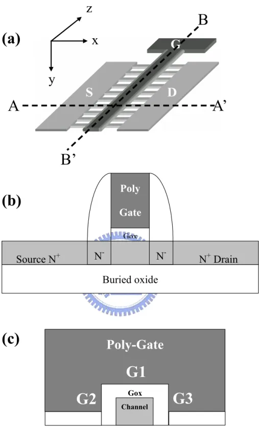
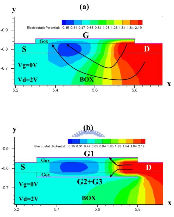
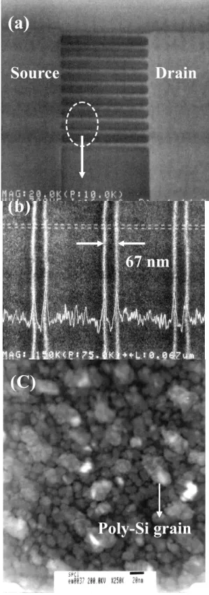
(34) 3-3. Multiple Nanowire Channels Device Structure The TFTs, with a gate length of 0.5 um, consisting of ten strips of multiple 67 nm wire channels (M10) TFT, and a single-channel structure (S1) with W = 1 um TFT, were fabricated. Figure 2a presents the structure of the M10 TFT. Figure 2b presents the cross-section of the M10 TFT perpendicular to the AA’ direction. This M10 TFT has a conventional top-gate LDD MOSFET structure. Figure 2c presents cross-section of the M10 TFT perpendicular to the BB’ direction, in which the channels were surrounded by the gate electrode as tri-gate structure. Figure 3 presents device electrical characteristics simulation results using the DESSIS software package from ISE. The double-gate TFT simulation results serve to tri-gate TFT due to the similar dimension. Figure 3a shows the encroachment of electrical field from drain side of S1 TFT. However, in Fig. 3b, M10 TFT can confine the electrical field due to its superior tri-gate control. Therefore, it is expected that the M10 TFT tri-gate structure can suppress effectively short channel effects. Figure 4a and 4b present the scanning electron microscope (SEM) photograph of the poly-Si active region of the M10 TFT, and the 67-nm-wide multiple nano-wire channels in the M10 TFT, respectively. Figure 4c presents a plane view of transmission electron micrograph (TEM) photograph of the active region of the proposed TFTs. The average grain size in the polysilicon channel formed by solid phase crystallization is approximately 30 nm.. 22.
(35) 3- 4. Multiple Channels Device Fabrication Process Step1. Substrate. 6-inch p-type single-crystal silicon wafers with (100) orientation were used as the starting substrate. After a standard cleaning procedure, silicon wafers were coated with 400-nm-thick thermally grown SiO2 in steam oxygen ambient at 1000ºC Step2. Poly-Si thin film formation . Undoped 50-nm-thick amorphous-Si layers were deposited by low pressure chemical vapor deposition (LPCVD) at 550ºC. The amorphous-Si films were recrystallized by solid phase crystallization (SPC) method at 600ºC for 24hrs in N2 ambient. After Ebeam direct writing and transformer couple plasma (TCP) etching, the device active region source, drain and multiple channels were formed. Step3. Gate oxide formation. After defining the active region, the wafers were cleaned in H2SO4/H2O2 and NH4OH/H2O2 solution to remove residue of polymer before gate oxide deposition. A buffered HF dip was performed to remove the native oxide on the silicon surface. Then, a 26-nm-thick layer of tetra-ethyl-ortho-silicate (TEOS) gate oxide was deposited by LPCVD at 7000C. The thickness of gate oxide was determined by N&K optical analyzer. Step4. Gate electrode formation.. 23.
(36) After deposition of gate insulators, 150-nm-thick poly-silicon films were formed immediately on the gate insulators by LPCVD at 620°C. The second poly-Si layers were patterned by EBeam lithography and transformer couple plasma (TCP) etching to define the gate electrode and to be the mask for self-aligned implantation. Step5. LDD and source/drain formation. After the gate definition, the implantation for lightly-doping source and drain was performed by phosphorous ions at a dosage of 5×1013 cm-2. A 200nm-thick TEOS was then deposited by LPCVD, and anisotropically etched by reactive ion etching (RIE) to form a sidewall spacer abutting the poly-Si gate. Next, the self-aligned source and drain regions were formed by phosphorous ions implantation at a dosage of 5×1015 cm-2. After the source and drain formation, doping activation was performed by rapid thermal anneal (RTA). Step6. Passivation layer and contact hole formation. After doping activation, a 300-nm-thick TEOS oxide layer was deposited by 2. LPCVD as the passivation layer. The 5×5 um contact holes were patterned by reactive ion etching (RIE) subsequently. Step7. Metallization. The 300-nm-thick aluminum layers were deposited by physical vapor deposition (PVD) and then patterned to form the gate, source and drain contact metal pads.. 24.
(37) Finally, the devices were sintered at 400°C in hydrogen ambient for 30 min. Step8. Passivation. It is well known that grain boundary passivation is very effective in improving the performance of poly-Si TFTs. Therefore, to reduce trap density and improve interface quality, wafers were immured in an NH3 plasma generated by plasma enhanced CVD (PECVD) for 1 hr.. 25.
(38) Fig. 3-1. The cross section view of the Fluorinated Silica Glass (FSG) Spacers Device Structure. 26.
(39) z. (a). B. x y. A’. A B’ Poly. (b). Gate Gox. Source N+. N-. N-. N+ Drain. Buried oxide. (c). Poly-Gate. G1 G2. Gox Channel. G3. Fig. 3-2. (a) Schematic diagram of M10 poly-Si TFT. (b) Cross-section view of Fig. 1a AA’ direction, as a conventional top-gate LDD MOSFET structure. (c) One of channel cross-section view of Fig. 1a BB’ direction, as a tri-gate structure. Active layer, gate oxide, and poly-gate thickness are 50 nm, 26 nm and 150 nm, respectively.. 27.
(40) (a). y. Gox. G D. S Vg=0V BOX. Vd=2V. x. (b). y S. S. Gox Gox. G1 D. Vg=0V. G2+G3. Vd=2V. BOX. x. Fig. 3-3. Simulation results of potential contour plots and electrical field lines of (a) single-top-gate TFT (b) tri-gate TFT with L = 0.5 um, gate oxide = 26 nm, channel thickness = 50 nm at Vg = 0 V, Vd = 2 V.. 28.
(41) (a) Source. Drain. (b) 67 nm. (C). W=67n. Poly-Si grain. Fig. 3-4. (a) Scanning electron microscopy (SEM) photography of active pattern with the source, the drain and multiple nano-wire channels of M10 TFT. (b) Magnified area of multiple nano-wire channels. The each nano-wire width is 67 nm. (c) Transmission electron microscopy (TEM) photography of poly-Si grains by solid phase crystallization. The average poly-Si grain size is about 30 nm.. 29.
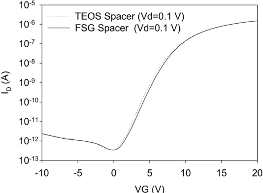
(42) Chapter 4 Experiment results and discussion In this chapter, the Poly-Si TFT with Self-aligned Fluorinated Silica Glass (FSG) Spacers is discussed in part I and the novel multiple nanowire Channels Poly-Si Thin-Film Transistors part is discussed in II.. Part I. Poly-Si TFT with Self-aligned Fluorinated Silica Glass (FSG) Spacers 4-1. Performance of Fluorinated and TEOS Spacers Poly-Si TFTs Figure 1 shows the Fourier transform infrared (FTIR) spectra of undoped SiO2 and FSG films between 400 cm-1 and 2000 cm-1. The FTIR spectra were measured from an unpatterned wafer with undoped SiO2 and FSG layer respectively. The main peak of function group Si-F is around 930 cm-1. The signal of Si-F bonds is clearly observed in the FSG film. Figures 4.2 (a) and 4.2 (b) show the comparison of transfers and output curves for poly-Si TFTs with TEOS and SiOF spacer. It is found the Id-Vg characteristics for Vd= 0.1 V of W/L=10um/5um in both types of poly-Si TFTs were nearly the same. This indicates the introduction of FSG spacer in poly-Si TFT device does not degrade electrical performance. In Id-Vd characteristics for Vg-Vth = 0,1,2,3,4 V, it is found that the kink effect 30.
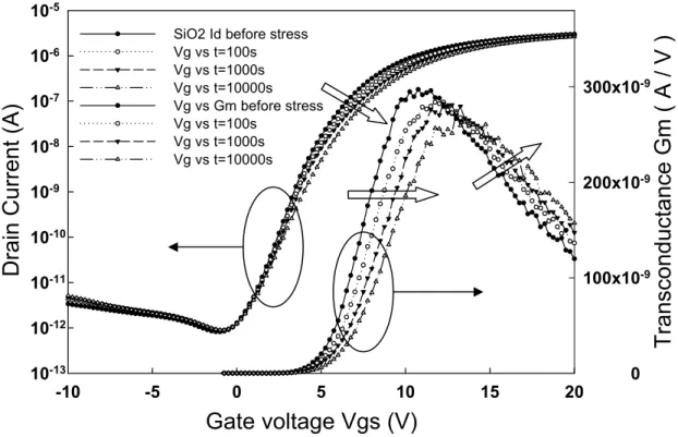
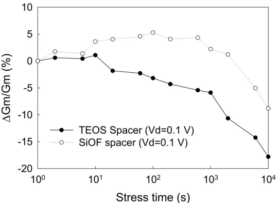
(43) occurs in both poly-Si TFTs. However, the drain current in the saturation region of TEOS spacer TFT is increasing more seriously than SiOF spacer TFT, especially at high gate voltages. The kink effect in poly-Si TFTs is attributed to channel avalanche multiplication occurred in the high fields near drain side, associated with the floating body effect. The suppression of kink effect for the poly-Si TFT with FSG spacers is more significant than the TEOS spacer poly-Si TFT. The fluorine ions in the sideward spacer near drain side strongly passivate the Si dangling bonds to avoid the occurrence of hot carriers.. 4-2. Reliability after DC stress of Fluorinated and TEOS Spacers Poly-Si TFTs In this work, the static stress is used to degrade the poly-Si TFT. The stressing bias of the gate potential Vgs and the drain potential Vds are fixed at 15V, and 30V, respectively. Figures 4.3(a) and 4.3(b) show the different degradation behaviors of drain current and trans-conductance between TEOS and FSG spacer under static stress, respectively. For TEOS spacer, the curve of the trans-conductance decreases monotonically and shows a parallel shift in the positive direction with the increase of the stress time. For FSG spacer, Gm,max is initially increased and then it starts to decrease after 1000 seconds stressing, while remains unchanged for Vgs > 17V. Figure 4.4 shows the degradation of the maximum trans-conductance defined as. 31.
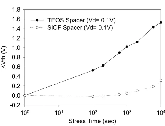
(44) ∆Gm,max/Gm,max0, where ∆Gm,max= Gm,max- Gm,max0, Gm,max0 is the initial transconductance and Gm,max is the transconductance after stress. Figure 4.5 shows the degradation of drain current at Vds=5V. The more serious degradation of TEOS spacer TFT in both Gm and Ion is found. This is due to the reducing of potential barrier in the channel by passivating the dangling bonds and traps in grain boundaries by fluorine ions. Figure 4.6 shows the threshold voltage variations (∆Vth) after stressing. In contrast with the large Vth shift for the TEOS spacer TFT, Vth shift for the SiOF spacer TFT was smaller. Vth is strongly dependent on the deep trap states which originate from the dangling bonds in the grain boundaries of the sideward channel [4-1]. The degradation of TEOS spacer TFT is due to deep states generated in the grain boundaries and at the gate oxide/channel interface with stress duration by breaking the weak and/or strained Si-H, Si-O bonds and even the strong Si-Si bonds[]. However, for SiOF spacer TFT, the superior reliability is due to the passivation of dangling bonds by fluorine ions near drain side. Since the dissociation energy of Si-F bonds is about twice of the Si-H bonds, Si-F is hardly broken by the stressing and thus generation of positive fixed charges in the gate oxide is suppressed[]. Moreover, the suppression of kink effect for the poly-Si TFT with FSG spacers also reduces the degree of degradation under the same stress condition.. 32.
(45) Figure 4.7 shows the comparison of the sub-threshold slope variation ∆SS characteristics of TEOS spacer TFT and SiOF spacer TFT for Vd= 0.1 V where ∆SS=SS - S0, S0 is the initial sub-threshold slope and S is the sub-threshold slope for each stress time. Initially, the ∆SS of SiOF spacer TFT is smaller than in the TEOS spacer TFT, but ∆SS is then rapidly degraded to approach the curve of TEOS spacer TFT after 6000 second. The sub-threshold swing varies with stress is also associated with the interface deep state generation, so less degradation in SiOF spacer TFT is due to the SiOF spacer TFT with better interface property at spacer regions near drain can reduce the variation of SS. But when the Si-F bonds formed only under sidewall spacers were broken in long term stress, SiOF spacer TFT loses the advantage of stronger passivation.. 33.
(46) Part II. Novel Multiple Nanowire Channels Poly-Si TFTs 4-3. Performance of Novel Multiple Nanowire Channels Poly-Si TFTs Figure 4.8 plots a typical normalized transfer curve and the field effect mobility of TFT devices with a single-channel and multiple nanowire channels, respectively. The transfer characteristics imply that the ON-state current of multiple nanowire channel TFTs is approximately similar to that of single-channel TFTs. This fact suggests that the single-channel and multiple nanowire channel TFTs can yield almost the same carrier mobility, indicating that the carrier mobility is not degraded in multiple nano-wire channel TFTs. Additionally, the leakage current of multiple nano-wire channels TFTs is reduced significantly as gate voltage (Vg) becomes more negative at Vd = 2 V, compared to the single-channel TFTs. The multiple nano-wire channels TFTs therefore has a higher current ON/OFF ratio (>108) than single-channel TFTs. Also, multiple nano-wire channel TFTs has a smaller subthreshold slope (SS), and is free of drain induced barrier lowering (DIBL), because they exhibit better gate control ability. The electrical characteristics of multiple nano-wire channel TFTs are also better because the width of each nano-wire channel is close to the size of a polysilicon grain, approximately 30 nm, as presented in Fig. 1c. Therefore, multiple nano-wire channels has fewer effective grain boundary defects than single-channel. 34.
(47) TFTs. Moreover, the effect of NH3-plasma passivation more efficiently affects multiple nano-wire channel TFTs than it does in single-channel TFTs, because the former has split nano-wire structures that are mostly exposed to NH3 plasma. Figure 3 depicts the output characteristics of single-channel TFTs with channel length (L) of 0.5 µm and width (W) of 1 um, as well as those of multiple nano-wire channel TFTs with channel length (L) of 0.5 µm and width (W) of 67nm×10 = 0.67 µm. The applied gate voltage was maintained at a constant value of Vg - Vth = 0.5, 1.0 and 1.5 V, to avoid that threshold voltages were different. The suppressed kink-effect was observed for multiple nano-wire channel TFTs, because they had fewer polysilicon grain boundary defects and exhibited more efficient NH3 plasma passivation. Table II lists the electrical parameters of the TFTs, including threshold voltage (Vth), subthreshold slope (SS), ON/OFF ratio and DIBL. Vth is defined as the gate voltage required to achieve a normalized drain current of Id = (W/L) × 10-7 A at Vd = 2 V. DIBL is defined as ∆Vg / ∆Vd at Id = 10-10 A. The effective trap state density (Nt) were extracted from the slope of ln ( Id / Vg ) versus (1 / Vg ) characteristics9 for devices with multiple and single-channel TFTs , to elucidate the effect of grain boundary defects on the performance of such TFT devices. In Fig. 4.10, multiple nano-wire channel TFTs exhibited a lower slope, indicating a lower effective trap state density (Nt ~ 1.81 × 10¹¹) than single-channel TFTs (Nt ~. 35.
(48) 2.12 × 10¹¹). This result is also consistent with the aforementioned comparison of the performance of multiple nano-wire channels with that of single-channel TFTs.. 4-4. Reliability after DC and AC stress of Novel Multiple Nanowire Channels Poly-Si TFTs The static hot carrier stress condition is determined at kink-effect occurrence, Vd = 6 V and Vg = 3V, and the source potential is common. The dynamic pulse train stress is defined at constant Vd = 6 V and dynamic Vg = 3V (high), 0V (low) with the duty cycle of 50%, and the source potential is common. The waveform of the pulse train is shown in Fig.4.11. In this section, we discuss the deceive reliability after a series of stress frequency (f), rising time (tr), falling time (tf) and substrate temperature conditions. Fig. 4-12 (a) depicts typical M10 poly-Si TFT Id-Vg curves before and after DC hot carrier stress at 10000 second. Fig.4.12 (b) depicts typical S1 poly-Si TFT Id-Vg curves before and after DC hot carrier stress at 10000 second. Figure 4-13 depicts trans-conductance degradation of S1 and M10 TFT as a function of the stress time with different frequencies (DC, f = 1K Hz, and f = 1M Hz). The S1 and M10 TFT show the similar Gm degradation. These results reveal that the S1 and M10 have similar tail state generation. Figure 4-14 and 4-15 depict the threshold voltage and subthreshold swing. 36.
(49) variation of S1 and M10 TFT as a function of the stress time with different frequencies, respectively. For M10 TFT the Vth and SS variation is much lower than the S1 TFT. The results indicate that the M10 TFT has less deep states. Firstly, the M10 TFT has more effective NH3 plasma passivation than that of S1 TFT due to the ten split nanowire channels of M10 TFT has wide NH3 plasma passivation area. Secondly, M10 TFT has robust tri-gate control, thus the additional two side-gate surface scattering (Fig. 3b) reduce the hot carrier effect. Therefore, the deep states generation of M10 TFT by the hot carrier impaction is lower than which of S1 TFT. Notably, for S1 TFT, the Vth and SS variation increase with the frequency increasing from 1 K Hz to 1 MHz. These results reveal that the device reliability is strongly dependent on the transient current Id (displace current). dVg ≈ Cox ⋅ f ⋅ Vg dt where f is frequency, Vg is average gate voltage. I d = Cox ⋅. Thus, the transient current induced hot carrier is dependent on the frequency. Figure 4-16 and 4-17 depict the ON current (ION) variation and ON/OFF ratio of S1 and M10 TFT as a function of the stress time with different frequencies, respectively. The M10 TFT shows lower ION variation than S1 TFT. These results reveal that the S1 TFT has high Vth variation and increase with the frequency increasing. Thus, the ION of S1 TFT is much lowering than that of M10 TFT. For the ON/OFF ratio, although the S1 and M10 TFT have the similar degradation behavior, 37.
(50) the ON/OFF ratio of M10 still remains exceed 108, under different frequencies. Figure 4-18 depicts Gm degradation of S1 and M10 TFT as a function of the stress time with different rising time (Tr) and falling time (Tf) under the frequency of 1 KHz. For S1 TFT (dash-line) with the same falling time of 100 ns, the S1 TFT has the similar Gm degradation. However, for the same rising time of 100 ns, as the falling time increasing from 100 ns to 1 us, the Gm degradation is reduced from 40% to 20% at the stress time at 1000 second. These results reveal that the device reliability is strongly dependent on the transient current. According to the Uraoka et al. report [4-2], only the transient current induced by the falling period would cause more damage near the drain. Figure. indicates clearly that the amount of the hot carriers. generated depends on the pulse falling time. Therefore, using the dynamic stress with longer falling time will be helpful for the reliability improvement in the poly-Si TFTs. On the other hand, for M10 TFT, however the Gm degradation dependent on falling time is not significant. These results indicate that M10 TFT has highly effective NH3 plasma passivation and robust tri-gate control to screen the transient current hot carrier effect, which induced by the falling period. Figure 4-20 and 4-21 depicts Vth variation and ON current (Ion) degradation of S1 and M10 TFT as a function of the stress time with different rising time (Tr) and falling time (Tf) under the frequency of 1 KHz. For the same reason, the Vth variation. 38.
(51) and ON current (Ion) degradation of S1 TFT (dash-line) is highly dependent on the falling time rather than rising time. As the falling time increasing from 100 ns to 1 us, the Vth variation and ON current (Ion) degradation are reduced. Again, M10 TFT has highly effective NH3 plasma passivation and robust tri-gate control to screen the transient current hot carrier effect, which induced by the falling period. Figure 4-22 depicts Gm degradation of S1 and M10 TFT as a function of the stress time with different subtract temperature with 250C, and 750C under the same frequency of 1 KHz, and the same Tr = Tf =100 ns. For both S1 and M10 TFT, the Gm degradation is reduced with the temperature increasing from 250C to 750C. These results reveal that hot carrier effect is reduced with the temperature increasing. As the temperature increasing, the mean free path (λ) [4-3] is decreasing.. λ = λ0 ⋅ tanh(. EP ) 2kT. Thus, that hot carrier energy is reduced as the mean free path (λ) is decreasing. Figure 4-23 and 4-24 depicts Vth variation and ON current (Ion) degradation of S1 and M10 TFT as a function of the stress time with 250C, and 750C under the same frequency of 1 KHz, and the same Tr = Tf =100 ns. For both S1 and M10 TFT, the Vth variation and ON current (Ion) degradation is reduced with the temperature increasing from 250C to 750C. For the same reason, hot carrier effect is reduced with the temperature increasing as the mean free path (λ) decreasing.. 39.
(52) 0.30 TEOS FSG (CF4=600sccm). Absorbance (a.u). 0.25 0.20. Si-O. Si-F. 0.15 0.10 0.05 0.00 -0.05 400. 600. 800 1000 1200 1400 1600 1800 2000 Wavenumber (cm-1). Figure4.1 FTIR Spectra of FSG film and TEOS film between 2000cm-1 and 400 cm-1. 40.
(53) 10-5 10-6. TEOS Spacer (Vd=0.1 V) FSG Spacer (Vd=0.1 V). 10-7 ID (A). 10-8 10-9 10-10 10-11 10-12 10-13 -10. -5. 0. 5. 10. 15. 20. VG (V) Figure4.2 (a) Comparsion of Id-Vg characteristics of FSG spacer TFT and TEOS spacer TFT for Vd=0.1 V (W/L=10um/5um). 80 TEOS Spacer FSG Spacer. ID (µA). 60. 40. 20. 0 0. 5. 10 VD (V). 15. 20. Figure 4.2 (b) Comparsion of output characteristics for FSG spacer and TEOS spacer TFT, W/L=10um/5um, VG-Vth= 0,1,2,3,4 V 41.
(54) 10-5. Drain Current (A). 10-7 10-8. Transconductance Gm ( A / V ). SiO2 Id before stress Vg vs t=100s Vg vs t=1000s Vg vs t=10000s Vg vs Gm before stress Vg vs t=100s Vg vs t=1000s Vg vs t=10000s. 10-6. 300x10-9. 200x10-9. 10-9 10-10. 100x10-9. 10-11 10-12 10-13 -10. -5. 0. 5. 10. 15. 20. 0. Gate voltage Vgs (V) Fig4.3 (a) The degradation of drain current and trans-conductance by static stress in TEOS spacer structure. 10-5. 10-7 10-8. Transconductance Gm ( A / V ). 10-6. Drain Current (A). 400x10-9. siof Id before stress Vg vs t=100s Vg vs t=1000s Vg vs t=10000s Vg vs Gm before stress Vg vs t=100s Vg vs t=1000s Vg vs t=10000s. 300x10-9. 10-9. 200x10-9. 10-10 10-11. 100x10-9. 10-12 10-13 -10. -5. 0. 5. 10. 15. 20. 0. Gate voltage Vgs (V) Figure 4.3 (b) The degradation of drain current and trans-conductance by static stress in SiOF spacer structure. 42.
(55) 10. ∆Gm/Gm (%). 5 0 -5 -10 -15 -20 100. TEOS Spacer (Vd=0.1 V) SiOF spacer (Vd=0.1 V) 101. 102. 103. 104. Stress time (s) Figure 4.4 Comparsion of ∆Gm/Gm characteristics of SiOF spacer TFT and TEOS spacer TFT for Vd=0.1V (W/L=10um/3um). 10x10-6 0 -10x10-6 -20x10-6 -30x10-6 -40x10-6. TEOS Spacer (Vd=5 V) SiOF Spacer (Vd=5 V). -50x10-6 -60x10-6. 101. 102. 103. 104. stress time (s) Figure 4.5 Comparsion of ∆Ion characteristics of SiOF spacer TFT and TEOS spacer TFT for Vd=5V (W/L=10um/3um) 43.
(56) 1.8 1.6. TEOS Spacer (Vd= 0.1V) SiOF Spacer (Vd= 0.1V). 1.4 ∆Vth (V). 1.2 1.0 0.8 0.6 0.4 0.2 0.0 -0.2 100. 101. 102 Stress Time (sec). 103. 104. ∆S.S. Figure 4.6 Comparsion of ∆Vth characteristics of FSG spacer TFT and TEOS spacer TFT for Vd=0.1V (W/L=10um/3um). 0.18 0.16 0.14 0.12 0.10 0.08 0.06 0.04 0.02 0.00 -0.02 -0.04. TEOS Spacer (Vd=0.1 V) SiOF Spacer (Vd=0.1 V). 102. 103. 104. Stress Time (sec) Figure 4.7 Comparison of ∆SS characteristics of SiOF spacer TFT and TEOS spacer TFT for Vd=0.1V (W/L=10um/3um) 44.
(57) 10-3. 60. Vd=2V. 10. -5. 10. -6. Multiple nano-wire channels Single channel. 50. Vd=0.05V. 10-7. 40. 10-8 10-9 30. 10-10 10-11. 20. 10-12 10-13. Field effect mobility (cm2/Vs). Drain current (A/um). 10-4. 10. 10-14 10-15 10-16 -5. -4. -3. -2. -1. 0. 1. 2. 3. 4. 5. 0. Gate voltage (V). FIG. 4.8. Comparison of Id-Vg transfer characteristics of multiple nano-wire channels (W/L = 67nm × 10/0.5um) and single-channel (W/L = 1um/0.5um) polysilicon TFTs.. Drain current (uA/um). Vg-Vth=1.5V. Multiple nano-wire channels Single channel. 15. 10. Vg-Vth=1.0V. 5. Vg-Vth=0.5V. 0. 0. 1. 2. 3. Drain voltage (V) FIG. 4.9. Comparison of Id-Vd output characteristics of multiple nano-wire channels (W/L = 67nm×10/0.5um) and single-channel (W/L = 1um/0.5um) polysilicon TFTs. 45.
(58) Table II Device parameters of single-channel TFTs with L/W = 0.5um/1um, and multiple nano-wire channels TFTs with L/W = 0.5um/67nm×10. All parameters were extracted at Vd = 2V, except for the field-effect mobilities which were extracted at Vd = 0.05V.. Single Channel Multiple channel. Mobility (cm2/VS). Vth (V). SS (mV/dec.). Ion / Ioff. DIBL (V/V). 34.01. -0.11. 360. 5.90 × 10⁷. 0.40. 32.50. 0.23. 110. 4.73 × 10⁸. 0. -15.2. -1 ln(Id/Vg) (AV ). -15.3. Nt ~ 1.81x10¹¹ (cm-2). -15.4 -15.5 -15.6. 11. -2. Nt ~ 2.12x10 (cm ) -15.7. Single-channel Multiple nano-wire channels. -15.8 -15.9. 1. 2. 3. 4. 1/Vg (V-1). FIG. 4.10 Effective trap state density of multiple nano-wire channels (W/L = 67nm×10/0.5um) and single-channel (W/L = 1um/0.5um) polysilicon TFTs.. 46.
(59) V Vd=6V. Tr. Tf. Vg=3V. Vg=0V. Vg=0V T=1/f. FIG. 4-11. The AC stress waveform of the pulse train.. 47. time.
(60) Drain current (A). 10-3 10-4 (b) 10-5 M10 TFT 10-6 W/L=67nmX10/0.5um 10-7 10-8 10-9 10-10 10-11 10-12 10-13 10-14 10-15 10-16 10-17 -5 -4 -3 -2 -1 0. Vd=2V Vd=0.05V. Before stress After DC 10000sec stress. 1. 2. 3. 4. 5. Gate voltage (V). Drain current (A). FIG. 4.12(a) Typical M10 poly-Si TFT Id-Vg curves before and after DC hot carrier stress at 10000 second.. 10-3 10-4 (a) 10-5 S1 TFT 10-6 L/W=0.5um/1um 10-7 10-8 10-9 10-10 10-11 10-12 10-13 10-14 10-15 -5 -4 -3 -2 -1 0. Vd=2V. Vd=0.05V Before stress After DC 10000 sec stress. 1. 2. 3. 4. 5. Gate voltage (V) FIG. 4.12(b) Typical S1 poly-Si TFT Id-Vg curves before and after DC hot carrier stress at 10000 second.. 48.
(61) 20 M10 DC S1 DC M10 f = 1KHz S1 f = 1KHz M10 f =1 MHz S1 f = 1 MHz. ∆Gm / Gm (100%). 0. -20. -40. -60. -80. 1. 10. 100. 1000. 10000. Stress time (sec) FIG. 4.13 Transconductance degradation of S1 and M10 TFT as a function of the stress time with different frequencies (DC, f = 1K Hz, and f = 1M Hz).. 3.0 M10 DC S1 DC M10 f = 1 KHz S1 f = 1 KHz M10 f = 1 MHz S1 f = 1 MHz. 2.5. ∆Vth. 2.0 1.5 1.0 0.5 0.0 -0.5. 1. 10. 100. 1000. 10000. Stress time (sec) FIG. 4.14. Teshold voltage of S1 and M10 TFT as a function of the stress time with different frequencies.. 49.
(62) 1.0 M10 DC S1 DC M10 f=1KHz S1 f=1KHz M10 f=1MHz S1 f=1MHz. ∆SS. 0.5. 0.0. -0.5. 1. 10. 100. 1000. 10000. Stress time (sec) FIG. 4.15. Subthreshold swing variation of S1 and M10 TFT as a function of the stress time with different frequencies.. ∆Ion / Ion (%). 0 -20 -40 M10 DC S1 DC M10 f=1kHz S1 f=1kHz M10 f=1MHz S1 f=1MHz. -60 -80 -100. 1. 10. 100. 1000. 10000. Stress time (sec) FIG. 4.16. ON current (ION) variation of S1 and M10 TFT as a function of the stress time with different frequencies. 50.
(63) 1010 109. Ion / Ioff. 108 107 M10 DC S1 DC M10 f = 1KHz S1 f = 1KHz M10 f = 1MHz S1 f = 1MHz. 106 105 104. 1. 10. 100. 1000. 10000. Stress time (sec) FIG. 4-17. ON/OFF ratio of S1 and M10 TFT as a function of the stress time with different frequencies.. ∆Gm / Gm (%). 0.0. -0.2. -0.4. M10 tr=tf=100ns S1 tr=tf=100ns M10 tr=1us tf=100ns S1 tr=1us tf=100ns M10 tr=100ns tf=1us S1 tr=100ns tf=1us. -0.6. -0.8 1. 10. 100. 1000. Stress time (sec). FIG. 4-18. Gm degradation of S1 and M10 TFT as a function of the stress time with different rising time (Tr) and falling time (Tf) under the frequency of 1 KHz. 51.
(64) Fig. 4-19. Dependence of emission intensity on (a) pulse rise time and (b) pulse fall time. Emission intensity is independent of the pulse rise time. However, we have found that it strongly depends on the fall time.. M10 tr=tf=100ns S1 tr=tf=100ns M10 tr=1us tf=100ns S1 tr=1us tf=100ns M10 tr=100ns tf=1us S1 tr=100ns tf=1us. ∆Vth. 0.5. 0.0 1. 10. 100. 1000. Stress time (sec) FIG. 4-20. Vth variation of S1 and M10 TFT as a function of the stress time with different rising time (Tr) and falling time (Tf) under the frequency of 1 KHz. 52.
(65) 0. ∆Ion / Ion (%). -10. -20. -30 M10 tr=tf=100ns S1 tr=tf=100ns M10 tr=1us tf=100ns S1 tr=1us tf=100ns M10 tr=100ns tf=1us S1 tr=100ns tf=1us. -40. -50. 1. 10. 100. 1000. Stress time (sec) FIG. 4-21. ON current (Ion) degradation of S1 and M10 TFT as a function of the stress time with different rising time (Tr) and falling time (Tf) under the frequency.. 0.2. ∆Gm / Gm (100%). 0.0. -0.2. -0.4 0. M10 25 C f=1kHz 0 S1 25 C f=1kHz 0 M10 75 C f=1kHz 0 S1 75 C f=1kHz 0 M10 125 C f=1kHz 0 S1 125 C f=1kHz. -0.6. -0.8 1. 10. 100. 1000. Stress time (sec) FIG. 4-22. Gm degradation of S1 and M10 TFT as a function of the stress time with different subtract temperature with 250C, and 750C under the same frequency of 1 KHz. 53.
(66) 0.8 M10 250C f=1KHz S1 250C f=1KHz M10 750C f=1KHz S1 750C f=1KHz M10 1250C f=1KHz S1 1250C f=1KHz. 0.7 0.6 0.5. ∆Vth. 0.4 0.3 0.2 0.1 0.0 -0.1 -0.2. 1. 10. 100. 1000. Stress time (sec) FIG. 4-23. Vth variation of S1 and M10 TFT as a function of the stress time with 250C, and 750C under the same frequency of 1 KHz.. 0. ∆Ion / Ion (%). -10 -20 -30. 0. M10 25 C f=1KHz S1 250C f=1KHz M10 750C f=1KHz 0 S1 75 C f=1KHz M10 1250C f=1KHz S1 1250C f=1KHz. -40 -50 -60. 1. 10. 100. 1000. Stress time (sec) FIG. 4-24. ON current (Ion) degradation of S1 and M10 TFT as a function of the stress time with 250C, and 750C under the same frequency of 1 KHz. 54.
(67) Chapter 5 Conclusion For the first part, we have proposed and successfully demonstrated the novel poly-Si TFT device with FSG film as the spacers to enhance the electrical characteristics due to fluorine passivation effect. The poly-Si TFT with FSG spacers exhibits superior endurance against hot carrier effect, leading to improved electrical reliability and suppressed kink effect than the TFT with TEOS SiO2 spacer. In addition, the manufacture processes are compatible with the conventional TFT process. This indicates our proposed poly-Si TFT with FSG spacers is a promising technology for application in the TFT-LCDs. In the second part, the performance and AC & DC reliability of multiple nanowire poly-Si TFTs are investigated. The experiment results reveal that the multiple nanowire poly-Si TFTs has higher performance than single-channel TFT, including a high ON/OFF current ratio, a low subthreshold slope, an absence of DIBL and favorable output characteristics. In static and dynamic hot-carrier stress experiments, the multiple nanowire poly-Si TFTs reduces the degradation of Vth, SS, Ion, On/OFF ratio and DIBL, 55.
(68) for all kind of frequency, rising time, falling time and temperature, compared to single-channel TFT. These high reliability results of multiple nanowire poly-Si TFTs can be explained by its robust tri-gate control and its superior channel NH3 passivation on the poly-Si grain boundary. The fabrication of this novel multiple nano-wire channel structure TFTs is easy and involves no additional processes. Such TFTs are thus highly promising for use in future high-performance poly-Si TFT applications.. 56.
(69) References. Chapter 1 [1.1] H. Oshima and S. Morozumi, “Future trends for TFT integrated circuits on glass substrates,” IEDM Tech. Dig., 157 (1989) [1.2] M. Stewart, R. S. Howell, L. Pires, and M. K. Hatalis, “Polysilicon TFT technology for active matrix OLED displays ,” IEEE Trans. Electron Devices, vol. 48, pp. 845-851, 2001 [1.3] H. Kuriyama et al., “An asymmetric memory cell using a C-TFT for ULSI SRAM,” Symp. On VLSI Tech., p.38, 1992 [1.4] T. Yamanaka, T. Hashimoto, N. Hasegawa, T. Tanala, N. Hashimoto, A. Shimizu, N. Ohki, K. Ishibashi, K. Sasaki, T. Nishida, T. Mine, E. Takeda, and T. Nagano, “Advanced TFT SRAM cell technology using a phase-shift lithography,” IEEE Trans. Electron Devices, Vol. 42, pp.1305-1313,1995. [1.5] K. Yoshizaki, H. Takaashi, Y. Kamigaki, T.asui, K. Komori, and H. Katto, ISSCC Digest of Tech., p.166, 1985 [1.6] N. D.Young, G. Harkin, R. M. Bunn, D. J. McCulloch, and I. D. French , “The fabrication and characterization of EEPROM arrays on glass using a low-temperature poly-Si TFT process,” IEEE Trans. Electron Devices, Vol. 43, pp. 1930-1936, 1996. [1.7] T. Kaneko, U. Hosokawa, N. Tadauchi, Y. Kita, and H. Andoh, “400 dpi integrated contact type linear image sensors with poly-Si TFT's analog readout circuits and dynamic shift registers,” IEEE Trans. Electron Devices, Vol. 38, pp. 1086-1093, 1991 [1.8] U. Hayashi, H. Hayashi, M. Negishi, T. Matsushita, Proc. of IEEE Solid-State Circuits Conference (ISSCC), p. 266 , 1998. [1.9] N.Yamauchi, U. Inava, and M. Okamura, “An integrated photodetector- amplifier using a-Si p-i-n.
(70) photodiodes and poly-Si thin-film transistors,” IEEE Photonic Tech. Lett, Vol. 5, pp. 319-321, 1993. [1.10] M. G. Clark, IEE Proc. Circuits Devices Syst, Vol. 141, 133 (1994) [1.11] Noriyoshi Yamauchi, Jean-Jacques J. Hajjar and Rafael Reif, “Polysilicon Thin-Film Transistors with Channel Length and Width Comparable to or Smaller than the Grain Size of the Thin Film,” IEEE Trans. Electron Devices, Vol. 38, pp 55-60, 1991 [1.12] Singh Jagar, Mansun Chan, M. C. Poon, Hongmei Wang, Ming Qin, Ping K. Ko, Yangyuan Wang, “Single Grain Thin-Film-Transistor (TFT) with SOI CMOS Performance Formed by Metal-Induced-Lateral-Crystallization,” IEDM Tech. Dig., pp. 293-296, 1999. [1.13] T. J. King and K. C. Saraswat, “Low-temperature fabrication of poly-Si thin-film transistors, ” IEEE Electron Device Lett, Vol. 13, pp. 309-311, 1992. [1.14] H. Kuriyama, S. Kiyama, S. Noguchi, T. Kuahara, S. Ishida, T. Nohda, K. Sano, H. Iwata, S. Tsuda, and S. Nakano, “High mobility poly-Si TFT by a new excimer laser annealing method for large area electronics,” IEDM Tech. Dig, Vol. 91, p. 563 (1991) [1.15]. Shigeto Maegawa, Takashi Ipposhi, Shigenobu Maeda, Hisayuki Nishimura, Tsutomu Ichiki, Motoi Ashida, Osamu Tanina, Yasuo Inoue, Tadashi Nishimura, Member, ZEEE, and Natsuro Tsubouchi “Performance and Reliability Improvements in Poly –Si TFT’s by Fluorine Implantation into Gate Poly-Si” IEEE TRANSACTIONS ON ELECTRON DEVICES, VOL. 42, NO. 6, JUNE 1995. [1.16] B.S.Doyle, S.Datta, M. Doczy, S Hareland, B.Jin, J.Kavalieros, T. Linton, A. Murthy, R. Rios, and R. Chau, “High Performance Fully-Depleted Tri-Gate CMOS Transistors” IEEE Electron Devices Letters, Vol. 2, No.4 pp.263-265,2003 [1.17] Gen Pei, Jakub Kedzierski, Phil Oldiges, Meikei Ieong,and Edwin Chih-Chuan Kan, “ Finfet Design Considerations Based on 3-D Simulation and Analytical Modeling” IEEE Trans. Electron Devices, Vol. 8, No.49, pp.1411-1419, 2002..
(71) Chapter 2 [2-1] “Mechanism of device degradation in n- and p-channel polysilicon TFTs by electrical stressing” 1990_EDL_ [2-2] W. B. Jackson, J. M. Marshall, and M. D. Moyer, “Role of hydrogen in the formation of metastable defects in hydrogenated amorphous silicon, ” Phys. Rev. B, vol. 39, pp. 1164-1179, 1989. [2-3 ] K. R. Hofmann, C.Werner,W.Weber, and G. Dorda, “Hot-electron and hole-emission effects in short n-channel MOSFETs,” IEEE Trans. Electron Devices, vol. 32, pp. 691–699, Mar. 1985. [2-4] Yoshiaki Toyota, Takeo Shiba, Member, IEEE, and Makoto Ohkura, Member, IEEE “A New Model for Device Degradation in Low-Temperature N-Channel Polycrystalline Silicon TFTs Under AC Stress” IEEE TRANSACTIONS ON ELECTRON DEVICES, VOL. 51, NO. 6, JUNE 2004 [2-5] F. V. Farmakis et al., “Grain and grain-boundary control of the transfer characteristics of large-grain polycrystalline silicon thin-film transistors, ”Solid-State Electron., vol. 44, pp. 913–916, 2000. [2-6]. G. A. Armstrong, S. Uppal, S. D. Brotherton, and J. R. Ayres, “Modeling of laser-annealed polysilicon TFT characteristics, ” IEEE Electron Device Lett., vol. 18, pp. 315–318, July 1997.. [2-7]. Kow Ming Chang, Yuan Hung Chung, Gin Ming Lin, Chi Gun Denh, and Jian Hong Lin, “Enganced Degradation in Polycrystalline Silicon Thin-Film Transistors under Dynamic Hot-Carrier Stress,” IEEE Electron, Device Lett., vol. 22,No. 10, pp. 475–477, October 2001.. [2-8] Satoshi Inoue, Hiroyuki Ohshima and Tatsuya Shimoda SEIKO EPSON CORPORATION, Base Technology Research Center Owa 3-3-5, Suwa, Nagano 392, Japan“Analysis of Threshold Voltage Shift Caused by Bias Stress in Low Temperature Poly-Si TFTs’’ 1997 IEEE, IEDM 97-527 [2-9]. “Analysis of threshold voltage shift caused by bias stress in low temperature poly-Si TFTs” 4.5_1997_IEDM_.
(72) [2-10] So Yamada,') Shin Yokoyama and Mitsumasa Koyanagi Research Center for Integrated Systems, “TWO-DIMENSIONAL DEVICE SIMULATION FOR AVALANCHE INDUCED SHORT CHANNEL EFFECT IN POLY-SI TFT” 1990 IEEE [2-11]. KUEING-LONG CHEN, STEPHEN A. SALLER, IMELDA A. GROVES, AND DAVID B. SCOTT MEMBER, IEEE, “Reliability Effects on MOS Transistors Due to Hot-Carrier Injection” IEEE JOURNAL OF SOLID-STATECIRCUITS, VOL. SC-20, NO. 1, FEBRUARY 1985. [2-12] Yukiharu Uraoka, Noboyuki Hirai, Hiroshi Yano, Tomoaki Hatayama, and Takashi Fuyuki, “Hot Carrier Analysis in Low-Temperature Poly-Si TFTs Using Picosecond Emission Microscope”, IEEE TRANSACTIONS ON ELECTRON DEVICES, VOL. 51, NO. 1, JANUARY 2004. Chapter 4 [4-1] I.W. Wu, T.Y. Huang, Warren B. Jackson, Alan G. Lewis, and Anne Chiang, IEEE Electron Device Letter, 12, 181(1991) [4-2] Yukiharu Uraoka, Noboyuki Hirai, Hiroshi Yano, Tomoaki Hatayama, and Takashi Fuyuk “Hot Carrier Analysis in Low-Temperature Poly-Si TFTs Using Picosecond Emission Microscope’’ IEEE TRANSACTIONS ON ELECTRON DEVICES, VOL. 51, NO. 1, JANUARY 2004 [4-3] S.M Sze “Physics of Semiconductor Devices” 2nd Edition.
(73) 簡歷. 姓名:馮立偉 性別:男 出生日期:中華民國六十九年十月八日 籍貫:高雄市 地址:高雄縣鳳山市福德街 143 巷 36 號 7 樓 學歷:國立中山大學物理系 88 年 9 月~92 年 6 月 國立交通大學電子工程研究所 92 年 9 月~94 年 6 月 碩士論文:新穎製程及新穎結構的複晶矽薄膜電晶體之可靠度研究 Reliability Study of Novel Process and Novel Structure Polysilicon Thin-Film Transistors.
(74)
數據
+7
相關文件
To investigate the characteristics of Tsongkhapa’s meditation thought, the study is divided into five parts: (1) introduction, (2) Tsongkhapa’s exposition of meditation practice,
雙極性接面電晶體(bipolar junction transistor, BJT) 場效電晶體(field effect transistor, FET).
In this thesis, we propose a novel image-based facial expression recognition method called “expression transition” to identify six kinds of facial expressions (anger, fear,
To solve this problem, this study proposed a novel neural network model, Ecological Succession Neural Network (ESNN), which is inspired by the concept of ecological succession
In this study, variable weights are added into the probabilistic density function of Elliptical Probabilistic Neural Network (EPNN), so that the kernel function can be adjusted
Through the help of this study, the inconvenient of insufficient information of biological pilot plant can be improved, the manufacture security can be promoted, and the
According to frequency response, filters can be divided into: (1) low-pass filter, (2) high-pass filter, (3) band-pass filter and band-stop filter.. This paper only chooses
This thesis focuses on the use of low-temperature microwave annealing of this novel technology to activate titanium nitride (TiN) metal gate and to suppress the V FB
