國 立 交 通 大 學
電子工程學系 電子研究所碩士班
碩 士 論 文
應用於超寬頻3.1-10.6 GHz之無線接收端之
低雜訊放大器之設計
An ultra-wideband CMOS LNA for 3.1 to
10.6 GHz wireless receivers
研究生: 陳懿範
指導教授: 荊鳳德 博士
應用於超寬頻3.1-10.6 GHz之無線接收端低雜訊放大
器之設計
An ultra-wideband CMOS LNA for 3.1 to 10.6 GHz
wireless receivers
研 究 生:陳懿範 Student: Yi-Fan Chen
指導教授:荊鳳德 博士 Advisor: Dr.Albert Chin
國立交通大學
電子工程學系 電子研究所碩士班
碩士論文
A Thesis
Submitted to Department of Electronics Engineering & Institute of Electronics College of Electrical and Computer Engineering
National Chiao Tung University in Partial Fulfillment of the Requirements
for the Degree of Master in
Electronics Engineering
May 2007
HsinChu, Taiwan, Republic of China
I
應用於超寬頻3.1-10.6 GHz之無線接收端之
低雜訊放大器之設計
學生: 陳懿範
指導教授: 荊鳳德 博士
國立交通大學
電子工程學系電子研究所
摘要
本論文研製一個應用於超寬頻3.1-10.6 GHZ的低雜訊放大器是採用電阻 -電容回授串接電感做輸入匹配,而在輸出端是用current buffer做匹配。本研 究是以0.18微米互補式金氧半製程實現。此低雜訊放大器是以三級放大為主架構, 第一級為RC-feedback with series inductive peaking結構,是為了增加頻寬, 第二級為cascode結構,可以增加平均順向增益(S21),第三級則是current buffer,主要是在輸出端做匹配。為了能在所應用的頻段內達到相對的平坦增益,在前兩 級中利用shunt peaking 的方法去實現。供應電壓VDD為1.8伏特時,整個電路功 率消耗約為17.02mW,及包含pad的情況下整個電路大小約為0.51 mm2 。本研究的 低 雜 訊 放 大 器 所 量 測 的 規 格 , 平 均 順 向 增 益 (S21) 在 3.1-10.6GHz 時 為 6.73dB-13.20dB,逆向隔離(S12)為-39dB以下,S11為-7dB以下,S22約為-9.6dB 以下,而平均雜訊指數約為5.3dB。
II
An ultra-wideband CMOS LNA for 3.1 to 10.6
GHz wireless receivers
Student: Yi-Fan Chen
Advisor: Dr. Albert Chin
Department of Electronics Engineering & Institute of Electronics
Nation Chiao Tung University
Abstract
A 3.1-10.6 GHZ low noise amplifier is applied for ultra-wideband, it introduces
RC feedback with series inductive peaking for input matching. And current buffer is
used for output matching. This research is fabricated in 0.18-μ m CMOS process.
Three amplified stages are formed for main topology in low noise amplifier. The first
stage introduces RC-feedback with inductive peaking configuration, it can improve
the bandwidth. The second stage introduces cascode configuration, it can improve the
average forward S21. The third stage introduces current buffer configuration, it is used
for output matching. Relatively flat gain is essential over the entire desired band. The
low noise amplifier introduces the shunt peaking to achieve the above purpose. The
total power dissipation of the chip is about 17.02mW at power supply 1.8 volt. The
chip size included pad is 0.51 mm2. The measurement result of this study expect that
the forward S21 is between 6.73dB and 13.20dB at 3.1-10.6GHz, the reverse isolation
S12 is under -39dB, the magnitude of S11 is under -7 dB, the magnitude of S22 is under
III
誌謝
本論文得以完成,首先要感謝我的指導老師 荊鳳德 教
授,在兩年的碩士研究生涯裡,給予我豐富的指導與照顧,
不論是研究上與生活裡都讓我在這兩年裡獲得許多的收
穫。
我還要感謝張慈學長、張國慶學長、王鴻偉學長與陳科
閔學長他們在研究上與學業上給我的幫助,讓我得以順利完
成碩士研究。也要感謝建宏學長、彬舫學長、軍宏學長、佩
諭、正彥以及實驗室大家,因為有你們的陪伴與支持,讓我
度過愉快又充實的這兩年。
最後,我要對我的父母獻上最高的敬意與謝意,感謝家
人們對我的栽培、支持與鼓勵,才讓我有機會能接觸這一切
並且完成我的學業與研究。
IV
Contents
Abstract (in Chinese)
………IAbstract (in English)
………...II誌謝
…………...………IIIContents
……….IVFigure Captions
……….VIChapter 1 Introduction
1.1 UWB CMOS Receivers
………..………….….11.2 Motivation
………3Chapter 2 Basic Concept in RF Design
2.1 Linearity in RF Circuits………4
2.1.1 The 1-dB Compression Point and third-Order Intercept point…………..………6
2.1.2 Cascaded Nonlinear Stages……….11
2.2 Noise
………122.2.1 Noise Figure……….…...12
2.2.2 Noise Figure of LNA………...16
2.2.3 Noise Figure of cascade LNA……….17
Chapter 3 How to design Basic Low-Noise Amplifiers
3.1 Consideration to design a LNA……….19
V
3.1.1 Stability………...19
3.1.2 Impedance Matching Networks………...21
3.2 Conventional LNA design
………...…………...273.2.1 Narrow band LNA design………...………27
3.2.2 Wide-band LNA design………..…28
Chapter 4 UWB CMOS LNA Design
4.1 Circuit topology
………...334.2 Design procedures
………...364.2.1 Noise analysis………..36
4.2.2 Input and output match………..…..41
4.2.3 Shunt peaking………..42
4.3 Simulation Results
………454.4 Measurements and Conclusions
………49Chapter 5 Summary
………...54References
……….55VI
Figure Captions
Chapter 1 Introduction
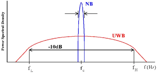
Fig. 1-1 The comparison with narrow band and UWB
Chapter 2 Basic Concept in RF Design
Fig. 2-1 The phenomenon of gain compression
Fig. 2-2 Definition of the 1-dB compression point
Fig. 2-3 The third-order intercept point
Fig. 2-4 Cascaded nonlinear stages
Fig. 2-5 Determination of input-referred noise voltage
Fig. 2-6 Representation of noise in a two-port network by equivalent
Chapter 3 How to design Basic Low-Noise Amplifiers
Fig. 3-1 Stability of two-port networks
Fig. 3-2 Circuit embedded in a 50-Ω system
Fig. 3-3 Circuit embedded in a 50-Ω system with matching circuit
Fig. 3-4 Example of a very sample matching network
Fig. 3-5 A possible impedance-matching network
Fig. 3-6 The eight possible impedance-matching networks with two reactive
components
VII
Fig.3-8 Common source stage use inductance degeneration
Fig.3-9 Wide-band LNA circuit schematic
Fig. 3-10 Small-signal equivalent circuit at the input
Fig.3-11 Another wide-band LNA schematic
Chapter 4 UWB CMOS LNA Design
Fig. 4-1 Circuits diagram
Fig. 4-2 The chip layout
Fig. 4-3 Noise model for the amplifying transistor M1
(a) M1 noise sources (b) Input-referred equivalent noise generators
Fig. 4-4 Equivalent circuit of the input stage for noise calculation
(a) one common design (b) this work.
Fig. 4-5 Noise figure: One common design v.s. This work
Fig. 4-6 Feedback configuration
Fig. 4-7 Model of shunt-peaked amplifier
Fig. 4-8 Simulated S11&S22
Fig. 4-9 Simulated S21
Fig. 4-10 Simulated NF
Fig. 4-11 Simulated S12
VIII Fig. 4-13 Two tones test
Fig. 4-14 Measured S21
Fig. 4-15 Measured S12
Fig. 4-16 Measured S11
Fig. 4-17 Measured S22
Fig. 4-18 Measured noise figure
Fig. 4-19 Measured linearity
1
Chapter 1
Introduction
1.1 UWB CMOS Receivers
Ultra-Wideband (UWB) is a technology for transmitting information spread
over a large bandwidth (>500 MHz) that should, in theory and under the right
circumstances, be able to share spectrum with other users.
Common Definitions
UWB: Total BW > 1.5 GHz , or Fractional bandwidth = fHf−fL
c > 25%. Narrowband: fHf−fL
c < 1%.
FCC Definition of UWB
Modulation type not specified, but the transmitted signal must meet the BW
requirements at all times during its transmission. So frequency hopping and frequency
swept systems are not allowed to meet the large bandwidth requirements. Systems
that achieve large bandwidth other than using pulses (such as very high rate DSSS)
are allowed.
Total BW > 500 MHz., Fractional bandwidth (measured at the -10dB points),
or fHf−fL
2
Fig. 1-1 The comparison with narrow band and UWB
From Fig.1-1, compare to traditional narrow band systems with
communication, UWB technology has the promising ability to provide extremely high
data rate performance in multi-user network applications, relativity immune to
multipath cancellation effects as observed in mobile and in-building environments,
and low interference to existing narrowband systems due to low power spectral
density. In other words, UWB has the advantages of low power consumption, low
cost (nearly “all digital”, with minimal RF electronics.), and a low probability of
detection (LPD) signature. Since the FCC has allocated 7.5 GHz of spectrum for
unlicensed use of UWB devices in the 3.1 to 10.6 GHZ frequency band, the low noise
amplifier needs to amplify the received UWB signal with sufficient gain and as little
as possible. Due to the electricity, noise and other parameters have strict demands, RF
3
(HBT), and PHEMT, etc to achieve these demands. In fact, in the past, most designer
introduces the GaAs process to design their products for GaAs excellent high
frequency parameter (like mobility), but with this work at [1] [2] [3], recently the
sub-micro CMOS process like 0.25 micrometer, 0.18 micrometer or 0.13 micrometer
CMOS process , reducing the minimum channel length and increasing the unity gain
cut off frequency, also has acceptable high frequency parameters. Besides, CMOS
process’s cost is cheaper than other process’s, we just focus on the CMOS technology.
[4]
1.2 Motivation
As wireless communications become wide-spread, our research aims to deliver
cost effective high-speed wideband applications with greater connectivity and
robustness. No matter what we produce with wireless communication technology,
such as cordless, cellular, global positioning satellite (GPS), wireless phones, wireless
local area network (LAN), wireless modems, and RFID tags, etc, those products all
need to use radio frequency communication. So how to develop the low power, low
cost, low noise radio frequency integrated circuits (RFIC) is very important. [5] Under
other chapters, I will discuss the basic concepts of RF design, some basic low-noise
amplifiers design for UWB step by step, and finally present my implementation of a
4
Chapter 2
Basic Concept in RF Design
2.1 Linearity in RF Circuits
Active RF devices are ultimately non-linear in operation. When driven with a
large enough RF signal the device will generate undesirable spurious signals. How
much spurious generated by the device is dependent on the linearity of the device.
Any nonlinear transfer function can be mathematically written as series
expansion of power terms unless the system contains memory. For simplicity, we
assume that:
Y t ≈ β0+ β1X t + β2X2 t + β3X3 t + ⋯ (2.1)
When a sinusoid uses in a nonlinear system, the integer multiples of the input
frequency will be exhibited by the output frequency components. For example, if X t = αcosωt, then
Y t = β0+ β1αcosωt + β2α2cos2ωt + β3α3cos3ωt + ⋯ (2.2)
It can be written as Y t = β0+β2α2 2 + β1+ 3β3α3 4 cosωt + β2α2 2 cos2ωt + β3α3 4 cos3ωt + ⋯ (2.3)
The term which has the input frequency is named as “fundamental” and the
higher-order terms the “harmonics”. We can observe that the amplitude of the nth
5
Two signals with different frequencies are applied to a nonlinear system,
called the two-tone test, is one common way to characterize the linearity of a circuit.
We assume that:
X(t) = x1 t + x2 t = α1cosω1t + α2cosω2t (2.4)
Apply this tone to (2.1), we can get
Y t = β0+ β1 (x1 (t) + x2 (t)) + β2 x1 t + x2(t) 2+ β3 x1 t + x2(t) 3+ ⋯
fundamental second-order third-order (2.5)
The output in general exhibits some components that are not harmonics of the
input frequencies. Called intermodulation (IM), this phenomenon arises from
multiplication of the two signals when their sum is raised to a power greater than
unity.
For example, the second-order terms can be expands as follows: x1 t + x2 t 2 = x1 t 2+ 2 x1 t x2 t + x2 t 2 (2.6) dc + HD2 IM2 dc + HD2
x1 t 2 term has a zero frequency (dc) and another at the second harmonic of the input (HD2),
x1 t 2 = α1cosω1t 2 = α1
2
2 1 + cos2ω1t (2.7)
6 Y t = β0+ β1 x1 t +x2 t + β2 x1 t 2 + 2 x1 t x2 t + x2 t 2 + β3 x1 t 3+ 3 x1 t 2 x2 t + 3 x2 t 2 x1 t + x2 t 3 + ⋯ (2.8) For amplifier, we desired only the terms at the input frequency. But expand
(2.8) by (2.4), discarding DC terms and harmonics, there still are intermodulation
products. ω → 2ω1± ω2:3β3α1 2α 2 4 cos 2ω1 + ω2 t + 3β3α12α2 4 cos 2ω1− ω2 t (2.9) ω → 2ω2 ± ω1:3β3α2 2α 1 4 cos 2ω2+ ω1 t + 3β3α22α1 4 cos 2ω2− ω1 t (2.10)
The mixing components (IM) will appear at the sum and difference
frequencies, in a typical two-tone test, α1=α2=α, and the ratio of the amplitude of the output third-order products to β1α defines the IM distortion. If a weak signal accompanied by two strong interferers experiences third-order nonlinearity, then one
of the IM products falls in the band of desired output if ω1 is close in frequency to ω2 and therefore cannot be easily filtered out. The effect is that third-order
nonlinearity can change the gain, which is seen as gain compression. And the two tone 2ω1 − ω2, 2ω2− ω1 are usually referred to as third-order intermodulation
terms (IM3 products). [6]
2.1.1 The 1-dB Compression Point and third-Order Intercept point
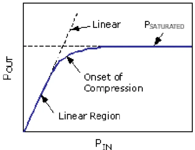
If an amplifier is driven hard enough the output power will begin to roll off
7
showed as Fig.2-1. The measurement of gain compression is given by the 1dB gain
compression point.
1dB Compression Point:
Like Fig.2-2, this parameter in one measure of the linearity of a device and is
defined as the input power that causes a 1dB drop in the linear gain due to device
saturation.
When operating within the linear region of a component, gain through that
component is constant for a given frequency. As the input signal is increased in power,
a point is reached where the power of the signal at the output is not amplified by the
same amount as the smaller signal. At the point where the input signal is amplified by
an amount 1 dB less than the small signal gain, the 1 dB Compression Point has been
reached. A rapid decrease in gain will be experienced after the 1 dB compression
point is reached. If the input power is increased to an extreme value, the component
will be destroyed. Passive, nonlinear components such as diodes also exhibit 1 dB
compression points. Indeed, it is the nonlinear active transistors that cause the 1 dB
compression point to exist in amplifiers. Of course, a power level can be reached in
any device that will eventually destroy it.
8
Fig. 2-1 The phenomenon of gain compression
Fig. 2-2 Definition of the 1-dB compression point
A common rule of thumb for the relationship between the 3rd-order intercept
point (IP3) and the 1 dB compression point (P1dB) is 10 to 12 dB. We will soon
discuss what IP3 is.
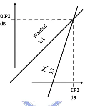
Third-Order Intercept point:
A third-order intercept point (IP3 or TOI) is another measure for weakly
nonlinear systems and devices, for example receivers, linear amplifiers and mixers. It
9
polynomial, derived by means of Taylor series expansion. The third order intercept
point relates nonlinear products caused by the 3rd order term in the nonlinearity to the
linearly amplified signal.
The third-order intercept point is a theoretical point where the amplitudes of
the fundamental tones at 2ω1− ω2 and 2ω2− ω1 are equal to the amplitudes of the fundamental tones at ω1 and ω2.
From (2.5), when ω1 = ω2 → x1(t) = x2(t) = xin, the fundamental (F) of the third-order terms can be written as:
F = β1xin +94β3xin3 (2.12)
The linear component can be written as:
F = β1xin (2.13) Compared to the third-order intermodulation term (IM3 =34β3xin3), since the
IM3 terms rises three times as the fundamental (60dB/decade to 20dB/decade) if xin
is small, we can define a theoretical voltage (xin = vIP3) when these two tones will be
equal: 3 4 β3vIP33 β1vIP3 = 1 (2.14) Therefore vIP3= 2 β1 3β3 (2.15)
10
Like Fig.2-3, the intercept point is obtained by plotting the output power
versus the input power on dB scale. The input power at this point is called the input
third-order intercept point (IIP3). If IP3 is specified at the output, it is called the output third-order intercept point (OIP3).
Fig. 2-3 The third-order intercept point
Two curves are drawn, one for the linearly amplified signal at an input tone
frequency, one for a nonlinear product. On a logarithmic scale, "x to the power of n"
translates into a straight line with slope of n. Therefore, the linearly amplified signal
will exhibit a slope of 1. A 3rd order nonlinear product will increase by 3 dB in power,
when the input power is raised by 1 dB. [7]
For instance, we have an output power called P1 at the fundamental frequency
11
have a slope 3 times as the fundamental terms (60dB/decade to 20dB/decade). Thus,
when The units of X-axis and Y-axis are dBm, OIP3 − P1
IIP3 − Pi = 1 and
OIP3 − P3
IIP3 − Pi = 3 (2.16) Assume a device has power gain G, and G can be measured as:
G = OIP3 − IIP3 = P1− Pi (2.17) So we can solve IIP3:
IIP3 = P1+1
2 P1− P3 − G = Pi+ 1
2 P1− P3 (2.18)
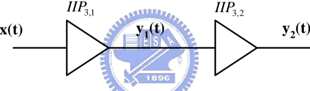
2.1.2 Cascaded Nonlinear Stages
Since in RF systems, signals are processed by cascaded stages, it is important
to know how the nonlinearity of each stage is referred to the input of the cascade.
Consider two nonlinear stages in cascade. As shown in Fig.2-4. Assuming that the
input-output relationship is ) ( ) ( ) ( ) ( 1 2 2 3 3 1 t x t x t x t y (2.19) ) ( ) ( ) ( ) ( 3 13 2 1 2 1 1 2 t y t y t y t y (2.20) Substitute (2.19) into (2.20) results in the relation
) ( ) 2 ( ) ( ) ( 3 3 3 1 2 2 1 1 3 1 1 2 t x t x t y (2.21) If we consider only the first- and third-order terms, then
3 3 1 2 2 1 1 3 1 1 3 2 3 4 IP A (2.22)
12
From equation (2.22) can be simplified if the two sides are inverted and
squared: 2 , 3 2 2 1 2 2 1 , 3 2 3 2 1 2 3 1 1 IP IP IP A A A (2.23)
where AIP3,1 and AIP3,2 represent the input IP3 points of the first and second
stages, respectively. From the above result, we note that as 1 increases, the overall
IP3 decreases. This is because with higher gain in the first stage, the second stage
senses larger input levels, thereby producing much greater IM3 products. [7]
1 3,
IIP
x(t)
y
1(t)
y
2(t)
2 3,IIP
Fig. 2-4 Cascaded nonlinear stages
2.2 Noise
2.2.1 Noise Figure
Noise is usually generated by the random motions of charges or charge
carriers in devices and materials. Because the noise process is random, one cannot
identify a specific value of voltage at a particular time, and the only recourse is to
characterize the noise with statistical measures, such as the mean-square or
13
need to simplify calculation of the total noise at the output. [8] Obviously, the
output-referred noise does not allow a fair comparison of the performance of different
circuits because it depends on the gain. According the circuit theory, we can use the
input-referred noise of circuits to represent the noise of behavior in the circuits. To
overcome the above confusion, we specify the “input-referred noise” of circuits.
Illustrate conceptually in Fig. 2-5. To represent the effect of all noise sources in the
circuit by a single noise source. The input-referred noise and the input signal are both
multiplied by the gain as they are processed by the circuit. Thus, the input-referred
noise indicates how much the input signal is corrupted by the circuit’s noise. The
input-referred noise is a spurious quantity in that in cannot be measured at the input of
the circuit. The two circuits of Figs. 2-5(a) and (b) are equivalent in mathematics but
the real physical circuit is still that in Fig. 2-5(b). The noise of a two-port network can
be modeled by two input noise sources: a series voltage source and a parallel current
source. Generally, the correlation between the two sources must be taken into account.
The situation is shown in Fig. 2-6, where a two-port network containing noise sources
is represented by the same network with internal noise sources removed and with a
noise voltage and current source connected at the input. It can be shown that this
representation is valid for any source impedance, provided that correlation between
14 1 2
In
2 2Vn
Vn ,
out
2
Noisy Circuit
(a)out
Vn ,
2
Noiseless Circuit
in Vn ,2 (b)Fig. 2-5 Determination of input-referred noise voltage
Noisy
network
R
s (a)Noiseless
network
R
s 2 iv
2 ii
(b)Fig. 2-6 Representation of noise in a two-port network by equivalent input voltage and current sources
15
The noise figure (F) describes quantitatively the performance of a noisy
microwave amplifier. The noise figure of a microwave amplifier is defined as the
ration of the total available noise power at the output of the amplifier to the available
noise power at the output due to thermal noise from the input termination R, where R is at the standard temperatureT = T0 = 290°K. The noise figure can be expressed in the form
F = PNo
PNiGA (2.24) PNo is the total available noise power at the output of the amplifier, PNi = kT0B is the available noise power due to R at T = T0 = 290°K in a bandwidth B, and GA is the available power gain.
GA can be expressed in the form
GA = PSo
PSi (2.25) PSo is the available signal power at the output, and PSi is the available signal power at the input, then noise figure can be written as
F = PSi PNi PSo PNo (2.26)
In other words, F can also be defined as the ratio of the available signal to
noise (SNR) power ratio at the input to the available signal-to-noise power ratio at the
16 reflection coefficient of the amplifier. [6]
2.2.2 Noise Figure of LNA
For LNA the total noise figure is basically determined by the noise figure of
the first stage of the LNA. The noise figure of a two-port amplifier is F = Fmin +rn
gs ys − yopt
2
(2.27) rn is the equivalent normalized noise resistance of the two-port, ys = gs + jbs represents the normalized source admittance, and yopt = gopt + jbopt represents the normalized source admittance which results in the minimum noise figure, call Fmin.
We can express ys and yopt in the terms of the reflection coefficients Γs and Γopt, thus
ys =1 − Γs 1 + Γs (2.28) And yopt = 1 − Γopt 1 + Γopt (2.29) So F can be written as F = Fmin + 4rn Γs − Γopt 2 1 − Γs 2 1 + Γopt 2 (2.30)
The noise resistance rn can be measured by reading the noise figure when Γs = 0, and the value Fmin, which occurs when Γs = Γopt, and the source reflection coefficient that produces Fmin can be determined accurately using network
17
analyzer. Fmin is a function of the device operating current and frequency, and there is one value of Γopt associated with each Fmin. [6]
For a given noise figure F = Fi , define the noise figure parameter Ni as Ni = Fi− Fmin
4rn 1 + Γopt
2
(2.31)
2.2.3 Noise Figure of cascade LNA
In the case of a two-stage (or n-stage) amplifier, the noise figure of the second
stage is reduced by GA1. Therefore, the noise contribution from the second stage is small if GA1 is large and can be significant if the gain GA1 is low. In a design, a trade-off between gain and noise figure is usually made. [6]
The quantity M is known as the noise measure, and be defined as
M = F − 1 1 − 1G
A
(2.32)
It expresses the fact the lowest total noise figure is not obtained with Γs = Γopt in each stage but with a value of Γs that minimizes each stage noise measure. In most designs, the values of GA are sufficiently large so that the value of Γs = Γopt that minimizes a given stage noise figure also minimizes its noise measure.
When two cascaded amplifier to determine which on should be used first in
order to achieve the lowest noise figure, we should use the lowest M to be the first.
18
achieved when the amplifier with the lowest value of M is connected at the input. For
the case of a chain of n amplifiers, the total noise figure is written as F = F1+F2− 1 GA1 + F3− 1 GA1GA2+ F4 − 1 GA1GA2GA3+ ⋯ (2.33) If the amplifiers are identical with F = F1 = F2 = ⋯ Fn and GA1 = GA2 = ⋯ = GAn, reduces to
F = 1 + F1− 1 1 − 1G
A1
19
Chapter 3
How to design Basic Low-Noise Amplifiers
3.1 Consideration to design a LNA
The most important design considerations in a microwave transistor amplifier
are stability power gain, bandwidth, noise, and dc requirements. It is important to
select the correct dc operating point and the proper dc network topology in order to
obtain the desired ac performance.
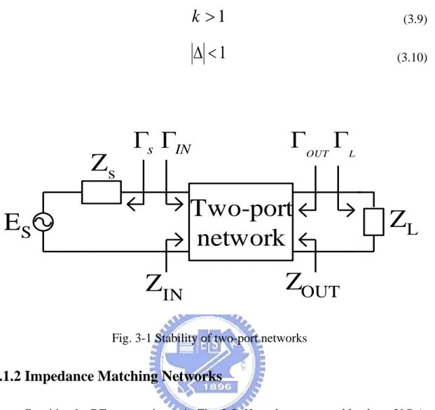
3.1.1 Stability
An unconditionally stable transistor will not oscillate with any passive
termination. On the other hand, a design using a potentially unstable transistor
requires some analysis and careful considerations so that the passive terminations
produce a stable amplifier.
The stability of an amplifier, or its resistance to oscillate, is a very important
consideration in a design and can be determined from the S parameters, the matching
networks, and the terminations. In a two-port network, oscillations are possible when
either the input or output port presents a negative resistance. In order to make it possible, ΓIN > 1 𝑜𝑟 ΓOUT > 1, and ΓIN and ΓOUT are defined as follows:
ΓIN = S11 + S12S21ΓL
20 ΓOUT = S22 + S12S21ΓS
1 − S11ΓS (3.2) If S12 = 0 that ΓIN = S11 and ΓOUT = S22 . Hence, if S11 > 1 the transistor presents a negative resistance at the input, and if S22 > 1 the transistor presents a negative resistance at the output.
The two-port network is shown in Figure 3-1. For unconditional stability any
passive load or source in the network must produce a stable condition. In terms of
reflection coefficients, the conditions for unconditional stability at a given frequency
are
Γs < 1 (3.3)
ΓL < 1 (3.4)
ΓIN < 1 (3.5)
ΓOUT < 1 (3.6)
We can get the required conditions for the two-port network to be
unconditionally stable by solving (3.3) to (3.6). [9]
21 2 1 2 2 2 2 2 11
2
1
S
S
S
S
k
(3.7) 21 12 22 11S
S
S
S
(3.8) Combine (3.1) and (3.2) to (3.7) and (3.8), a convenient way of expressing the21
1
k
(3.9)1
(3.10)Fig. 3-1 Stability of two-port networks
3.1.2 Impedance Matching Networks
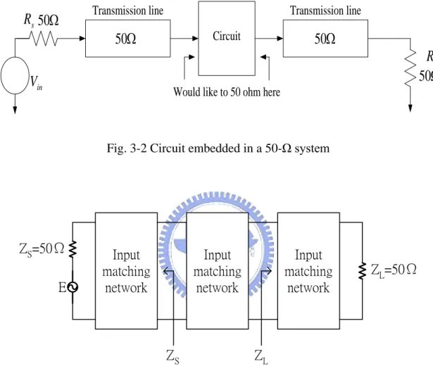
Consider the RF system shown in Fig. 3-2. Here the source and load are 50Ω (a
very popular impedance), as are the transmission lines leading up to the IC. For
optimum power transfer, prevention of ringing and radiation, and good noise
behavior,
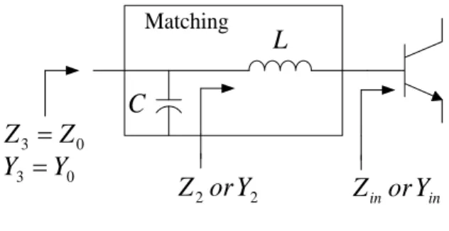
Fig. 3-3 illustrates a typical situation in which a transistor, in order to deliver
maximum power to 50Ω load, must have the terminations Zs and ZL. The input
matching network is designed to transform the generator impedance (show as 50Ω) to
the source impedance Zs, and the output matching network transforms the 50Ω
E
S
Z
s
s
INZ
IN
Two-port
network
OUT
L
Z
OUT
Z
L
22 termination to the load impedance ZL.
If a broadband matching is required, then other techniques may need to be used.
An example of matching a transistor amplifier with a capacitive input is shown in
Fig.3-4. Typically, reactive matching circuits are used because they are lossless and
because they do not add noise to the circuit will only be matched over a range of
frequencies and not at others. The series inductance adds an impedance of jL to cancel the input capacitive impedance. Note that, in general, when impedance is
complex
R jX
. Then to match it, the impedance must be driven from its complex conjugate
R jX
.A more general matching is required if the real part is not 50Ω. For example, if the real part of Z is less than 50Ω, then the circuit can be matching using the in
circuit in Fig. 3-5.
Series components will move the impedance along a constant resistance circle
on the Smith Chart. Parallel components will move the admittance along a constant
conductance circle. The input impedance of a circuit can be any values. In order to
have the best power transfer into the circuit, it is necessary to match this impedance to
the impedance of the source driving the circuit. The output impedance must be
similarly matched. It is very common to use reactive components to achieve this
23
series or parallel inductance or capacitance can be added to the circuit to provide an
impedance transformation.
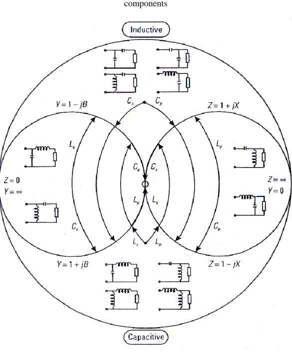
Although many different types of matching networks can be designed, the eight
Ell sections (also denotes as L sections) shown in Figure 3-6 are not only simple to
design but quite practical. The matching networks are lossless in order not to dissipate
any of the signal power.
In any particular region on the Smith Chart, several matching circuits will work
and others will not. This is illustrated in Figure 3-7, which shows what matching
networks will work in which regions. Since more than one matching network will
work in any region, how does one choose? There are a number of popular reasons for
choosing one over another.
1. Sometimes matching component can be used as dc blocks (capacitors) or to
provide bias currents (inductors).
2. Some circuits may result in more reasonable component values.
3. Personal preference. Not to be underestimated, sometimes when all paths
look equal, you just have to shoot from the hip and pick one.
4. Stability. Since transistor gain is higher at lower frequencies, there may be a
low-frequency stability problem. In such a case, sometimes a high-pass
24
5. Harmonic filtering can be done with a lowpass matching network (series L,
parallel C). This may be important, for example, for power amplifiers. [7]
50
Circuit50
50
50
lR
inV
Transmission line Transmission line
Would like to 50 ohm here s
R
Fig. 3-2 Circuit embedded in a 50-Ω system
E Input matching network Input matching network ZS Input matching network ZL ZS=50Ω ZL=50Ω
Fig. 3-3 Circuit embedded in a 50-Ω system with matching circuit
Matching 30 j 50 in Z 30 50 j
25 L C Matching 0 3 Z Z 0 3 Y Y 2 2orY Z Zin orYin Fig. 3-5 A possible impedance-matching network
s L Z p C s L Z p L s C Z p L s C Z p C Z p C s L Z Z Z p C s L p L s C p L s C
26 components
27
3.2 Conventional LNA design
3.2.1 Narrow band LNA design
In the design of low noise amplifier, there are many important goals. These
include noise figure minimization, providing sufficient gain with good linearity, and
the reasonable power consumption. Fig. 3-8 illustrates the input stage of the low noise
amplifier with source degeneration. A simple calculation is
s gs m gs s g in L C g sC L L s Z 2 2 2 1 ) ( (3.11)
If choose appropriate value of inductance and capacitance, then Lg+Ls and Cgs
will resonate at certain frequency. By choosing Ls appropriately, the real term can be
made equal to 50Ω . The gate inductance Lg is used to set the resonance frequency
once Ls is chosen to satisfy the criterion of a 50Ω input impedance. The matching
method in noise performance is better than using resistance termination of the input
end.
The reverse isolation of low noise amplifier determines the amount of LO
signal that leaks from the mixer to the antenna. The leakage arises from capacitive
paths, substrate coupling, and bond wire coupling. In heterodyne receivers with a high
first IF, the image-reject filter and the front-end duplexer significantly suppress the
28
leakage is attenuated primarily by the LNA reverse characteristics. Equation (3.7)
suggests that stability improves as S12 decrease, i.e., as the reverse isolation of the
circuit increases. The feedback can be suppressed through the use of a cascade
configuration, but at the cost of a somewhat higher noise figure. The common-gate
transistor in the Fig.3-8, M1, plays two important roles by increasing the reverse
isolation of the LNA: (1) it lowers the LO leakage produced by the following mixer,
and (2) it improves the stability of the circuit by minimizing the feedback from the
output to the input [10].
3.2.2 Wide-band LNA design
From Fig.3-9, the Rf is added as a shunt feedback element to the conventional
cascade narrow band LNA and Lload is used as shunt peaking inductor at the output.
The capacitor Cf is used for the ac coupling purpose. The source follower composed
of M3 and M4, is added for measurement proposes only, and provides wideband
output matching. C1 and C2 are ac coupling capacitor. The small-signal equivalent
circuit at the input of the LNA is shown in Fig. 3-10. The resistor RfM Rf /(1Av) represents the Miller equivalent input resistance of Rf, where Av is the open-loop
voltage gain of the LNA. From equivalent circuit, the value of Rf can be much larger
than that of the conventional resistance shunt-feedback. In the conventional resistance
29
of the key roles of the feedback resistor Rf is to reduce the Q-factor of the resonating
narrowband LNA input circuit. The Q-factor of the circuit shown in Fig. 3-10 can be
approximately given by gs fM g S T S WB
C
R
L
L
R
Q
0 2 0)
(
1
(3.12)From (3.12), and considering the inversely linear relation between the -3dB
bandwidth and the Q-factor, the narrowband LNA in Fig.3-9 can be converted into a
wideband amplifier by the proper selection of Rf. To design a wideband amplifier that
covers a certain frequency band, the narrowband amplifier will be optimized at the
center frequency. The feedback resistor Rf also provides its conventional roles of
flattening the gain over a wider bandwidth of frequency with much smaller noise
figure degradation [11].
Another wide-band LNA design schematic is shown in Fig.3-11. In Fig.3-11, is
the LNA circuit schematic. We discuss this circuit step by step from the first stage. First, to make1/gm 50, the gm value of common gate amplifier is going to be fixed at certain trans-conductance. An additional stage is required to provide sufficient gain
over the desired band. A shunt feedback common source amplifier is used in the
30
condition of the M1 to yield ReZ11 1/gm 50. This ensures input matching condition for wide-band of frequency. But this condition is violated with optimum
noise condition. There is a trade-off between noise and impedance matching in the
LNA circuit. One of the major problems in the wide bandwidth amplifier design is the
limitation imposed by the gain-bandwidth product of the active device. We know that
any active device has a gain roll off at high frequency because of the gate-drain and
gate-source capacitance in the transistor. This effect degrades the forward gain as the
frequency increases and eventually the transistor stops functioning as an amplifier at
the high frequency. Therefore the second design step is the selection of optimal bias
point of second stage of LNA so that it operates at its maximum fT. In addition to this
21
S degradation with frequency other complications that arises in wide-bandwidth amplifier design includes, increase in reverse gain S12 and noise figure at high frequency. Negative feedback configuration is used to reduce these effects and
increase the bandwidth. An inductor L is connected in series with Rf such that after
certain frequency the negative feedback decreases in proportion to the S21 roll-off.
This technique improves gain flatness at high frequency. The load inductance of L1
and L2 replace the resistor load which is used conventionally. The magnitude of the
inductor’s impedance increases as frequency increases. This increase inductor
31 frequency [12]. Lg Ls ZIN M1 M2
Fig.3-8 Common source stage use inductance degeneration
Fig.3-9 Wide-band LNA circuit schematic
Lg C1 Rbias Vg1 Ls Lload Rload M1 M2 M3 M4 C2 Rf Cf IN OUT VDD VDD Vg2
32
R
SL
gR
fMC
gs s TL
L
sFig. 3-10 Small-signal equivalent circuit at the input
Fig. 3-11 Another wide-band LNA schematic
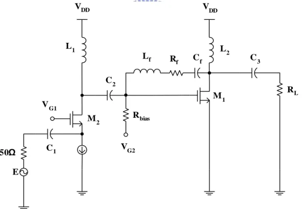
E VDD VDD VG1 VG2 M 2 M1 50Ω C1 C 2 Cf C3 Rbias Rf Lf L 1 L2 RL
33
Chapter 4
UWB CMOS LNA Design
4.1 Circuit topology
In designing a broadband amplifier, feedback and distributed configuration are
most widely used. In the chapter, feedback configuration was used instead of
distributed configuration because it is more adequate for integration due to better
uniformity and stability at frequencies below 12GHz. In addition, the cascode
structure has been considered as the best topology for wideband applications because
of its advantages
We design UWB LNA with cascode R-C feedback structure that the R-C
feedback connected between input and Lg, like Fig. 4-1. From Fig. 4-1, we can
observe that this is a three stage low noise amplifier. First stage used the cascode R-C
feedback structure. The advantages of cascode structure are high gain, wider
bandwidth, better stability and reverse isolation. The cascode configuration is being
used to reduce the high frequency roll-off of the input devices due to the Miller effect.
It can also be performed the input/output matching independently. The R-C feedback
(Rf & Cf) in cascode circuit improves the S11 of the circuit and stabilizes the
common-gate without reducing the gain. Above all, it can satisfy the requirements of
34 resistance.
The MOS M1 dominates the noise performance. These two MOS (M1 and M2)
have little effects with each other. This LNA for UWB applications was designed
using TSMC 0.18um RF CMOS technology and Fig. 4-2 shows the chip layouts.
35
36
4.2 Design procedures
4.2.1 Noise analysis
Three main contributors determine the noise performance of the R-C cascode
feedback topology: the gate inductor Lg, the feedback resistor Rf and the noise of the
amplifying device M1. We optimize the noise contribution from M1 relies on the
choice of its width for a given bias current.
MOS transistor noise sources are shown in Fig. 4-3(a). The noise generator i2 d is i2 d = 4kT 2 3gm Δf + k ia D f Δf (4.1)
4kT 23gm Δf is thermal noise component, and ki
a D
f Δf is flicker noise
component. And noise generator i is 2g i2 g
= 2qIGΔf (4.2) The input-referred in a conventional way and replaced with two correlated
noise generators, as shown in Fig. 4-3(b), because the current gain of the source degeneration is β jω =ωjωT, and the cutoff frequency is ωT ≈Cgm
gs, so i 2 ia is i2 ia = i2 g +jωCgs gm i 2 d (4.3) And v is 2ia v2 ia =i2 d gm (4.4) One common design that the R-C feedback connected between Lg and
37
MOS1’s gate (Fig. 4-4(a)) and this work (Fig. 4-4(b)) are showed below, and we can
compare with their equivalent circuit of the input stage for noise calculation.
In Fig. 4-4(a), the feedback of the common design topology:
vib1 via (4.5) iib1 iia if (4.6) Then,
vi1 vib1iib1RLg vLg via iia RLg vLg if RLg (4.7) ii1 iib1 iia if (4.8) Thus, the total equivalent noise voltage and current of this feedback is
v2i1 v2ia v2Lg i2ia RLg2 i2f RLg2 (4.9)
i2i1 i2ia i2f (4.10)
In Fig. 4-4(b), the feedback of this work topology:
vib2 viaiiaRLg vLg (4.11) iib2 iia (4.12) Then, vi2 vib2 viaiiaRLg vLg (4.13) ii2 iib2if iia if (4.14) Thus, the total equivalent noise voltage and current of this feedback is
38 v2i2 v2ia v2Lg i2iaRLg2 (4.15) i2i2 i2ia i2f (4.16) where f R kT i f f 1 4 2 (4.17) f kTR v Lg 4 Lg 2 (4.18)
The noise factor is
f R kT i f kTR v F S i S i 1 4 4 1 2 2 (4.19)
From equation (4.11) and (4.15), we can observe that the total noise of the
common design is greater than this work due to the
i
2f
R
Lg2 item. Fig. 4-5 showsthe noise figure: the common design versus this work. We can observe that the noise
figure of the topology of this work is better than the common one.
39 (b)
Fig. 4-3 Noise model for the amplifying transistor M1 (a) M1 noise sources (b)
Input-referred equivalent noise generators
40 (b)
Fig. 4-4 Equivalent circuit of the input stage for noise calculation
(a) one common design (b) this work
41
4.2.2 Input and output match
Input matching:
In feedback topology, the small signal equivalent is shown in Fig. 4-6, where
1 1 ' gs g in sL sC Z (4.20) 1 1 ,eff m 1 m m g g g (4.21) 1 1 d d L R sL Z (4.22) f f f R sC Z 1 (4.23) For this configuration, the input impedance and the gain can be
calculated to be in V f f in in Z A Z Z Z Z ' ) 1 ( ' (4.24) f L L f eff m L V Z Z Z Z g Z A , (4.25)
Since the circuit parameters Z ' and in A are frequency dependant, the V
characteristics of Z will vary accordingly over the frequency band. Thus, select f
f
Z and combination of R、C components,perfect matching and gain can be
achieved.
Output matching:
The third stage is decided to use source follower buffer to make 1 50 4
m
g 𝛺
42
Fig. 4-6 Feedback configuration
4.2.3 Shunt peaking
A model of shunt peaking amplifier is shown in Fig. 4-7. The capacitance C
may be taken to represent all the loading on the output node, including that of a
subsequent stage. The resistance R is the effective load resistance at that node and the
inductor provides the bandwidth enhancement. It’s clear from the model that the transfer function
in out
i v
is just the impedance of the RLC network, so it should be
straightforward to analyze. The addition of an inductance in series with the load
resistor provides an impedance component that increases with frequency, which helps
offset the decreasing impedance of the capacitance, leaving net impedance that
remains roughly constant over a broader frequency range than that of the original RC
network. The impedance of the RLC network may be written as
1 1 )] / ( [ 1 // ) ( 2 sRC LC s R L s R sC R sL s Z (4.26) dL must be sizable to have large gain and must be small so that it resonates
out
C out of band. R is chosen to place the zero frequency (d
d d z L R ) as close as
43 to the lower edge of the band to improve the gain.
We introduce a factor m, defined as the ratio of the RC and L/R time constant:
R L RC m / (4.27) Then, the transfer function becomes
1
)
1
(
1
1
)]
/
(
[
)
(
2 2 2
m
s
m
s
s
R
sRC
LC
s
R
L
s
R
s
Z
(4.28) where =L/R.The magnitude of the impedance, normalized to the DC value as a function of
frequency, is then 2 2 2 2 2
)
(
)
1
(
1
)
(
)
(
m
m
R
j
Z
(4.29) so that)
1
2
(
)
1
2
(
2 2 2 2 1
m
m
m
m
m
(4.30)where 1 is the uncompensated -3dB frequency. Because the load is
designed to achieve flat gain over the whole bandwidth, chosem1 2 2.414, then can lead to a bandwidth that is about 1.72 times as large as the un-peaked case.
Therefore, both a maximally flat response and a substantial bandwidth extension can
44
45
4.3 Simulation Result
Fig.4-8 shows the simulated input and output reflection coefficients. S11 is
lower than -10dB between 3.1 and 10.6GHz. The output buffer achieves excellent
matching such that S22 is lower than -12.57dB from 3.1GHz to 10.6 GHz. Fig. 4-9 is
the power gain versus frequency, and the maximum power gain is 18.43dB in our
simulation results. Since the output source follower drives a matched load, the voltage
gain of the core amplifier is exactly 6dB higher than S21. The -3dB bandwidth is
0.4~9.9GHz for the simulation. The noise figure (NF) of this UWB LNA is shown in
Fig.4-10. The noise figure is as low as 2.8dB at 10.6GHz, while the average noise
figure in-band is about 3.7dB. Fig.4-11 and 4-12 show the simulated reverse isolation
S12 and stability factor respectively. The two-tone test results for third-order
intermodulation distortion are shown in Fig.4-13. The test is performed at 5.5GHz.
IIP3 is to 5.19dBm, and the input referred 1-dB compression point (ICP) is -2dBm.
These results imply excellent linearity of our LNA. The proposed UWB LNA
46
Fig. 4-8 Simulated S11&S22
Fig. 4-9 Simulated S21 m1 freq= dB(S(2,1))=16.3143.100GHz m2 freq= dB(S(2,1))=16.028 10.60GHz m11 freq= dB(S(2,1))=17.2747.100GHz m3 freq= dB(S(1,2))=-62.5873.100GHz m4 freq= dB(S(1,2))=-47.087 10.60GHz 2 4 6 8 10 12 14 0 16 -100 -50 0 -150 50 freq, GHz d B (S (2 ,1 )) Readout m1 Readout m2 Readout m11 d B (S (1 ,2 )) Readout m3 Readout m4 m5 freq= dB(S(1,1))=-11.896 3.100GHz m6freq= dB(S(1,1))=-10.35410.60GHz m7 freq= dB(S(2,2))=-12.5743.100GHz m8 freq= dB(S(2,2))=-24.783 10.60GHz m12 freq= dB(S(1,1))=-10.1215.900GHz 2 4 6 8 10 12 14 0 16 -25 -20 -15 -10 -5 -30 0 freq, GHz d B (S (1 ,1 )) Readout m5 Readout m6 Readout m12 d B (S (2 ,2 )) Readout m7 Readout m8 m9 freq= nf(2)=4.4423.100GHz m10 freq= nf(2)=2.77710.60GHz 2 4 6 8 10 12 14 0 16 4 6 8 10 2 12 freq, GHz n f( 2 ) Readout m9 Readout m10 2 4 6 8 10 12 14 0 16 2 4 6 8 10 0 12 freq, GHz M u 1 M u P ri m e 1 EqnPdc_mw=I_Probe1.i*1.8*1000 Pdc_mw 21.844 2 4 6 8 10 12 14 0 16 5 10 15 0 20 freq, GHz d B (S (2 ,1 )) Readout m1 Readout m2 Readout m11 m1 freq= dB(S(2,1))=16.639 3.100GHz m2 freq= dB(S(2,1))=15.628 10.60GHz m11 freq= dB(S(2,1))=18.430 7.100GHz
47
Fig. 4-10 Simulated NF
48
Fig. 4-12 Simulated stability
49
4.4 Measurements and Conclusions
The following Fig.4-14 ~ Fig.4-19 are the measurement result which are
slightly different from simulation. Which imply good accuracy of simulation and
good circuit design. The some of the gain compression at high frequency showing in
Figure 4-14 maybe due to the underestimate of the load resistor parasitic.
The bandwidth of this work with considering matching and gain is from 3.1 to
10.6 GHz, while the average gain is about 10dB. Fig. 4-16 shows the measurement
result of S11 and the Fig. 4-17 shows the measurement result of S22. Output matching
is achieved well from 3.1 to 10.6 GHz. The average S11 is about -8dB and the S22
can bellow -9.6dB. Fig. 4-18 shows the measured noise figure. The noise performance
is very flat and the minimum noise figure is 5.03dB at 7GHz. The noise figure can be
better if we solve the resistor parasitic. Fig.4-20 shows the die photo of this circuit.
Total power consumption is 17mw which the vg is 0.7V and vdd1 and vdd2 are 1.8v.
Table 4.1 is the measurement result summary. By the capacitor-resistance feedback
with series inductive peaking we proposed, a good input and output matching,
broadband, a low power consumption amplifier is developed for UWB system
50 Fig. 4-14 Measured S21 Fig. 4-15 Measured S12 2 4 6 8 10 12 14 0 16 0 5 10 -5 15 freq, GHz d B (S (2 ,1 )) Readout m1 Readout m2 Readout m8 m1 freq= dB(S(2,1))=13.2043.100GHz m2 freq= dB(S(2,1))=6.737 10.60GHz m8 freq= dB(S(2,1))=13.8394.200GHz 2 4 6 8 10 12 14 0 16 -45 -40 -35 -30 -50 -25 freq, GHz d B (S (1 ,2 )) 3.100G -39.17 m9 10.60G -43.10 m10 m9 freq= dB(S(1,2))=-39.172 3.100GHz m10freq= dB(S(1,2))=-43.098 10.60GHz
51 Fig. 4-16 Measured S11 2 4 6 8 10 12 14 0 16 -12 -10 -8 -6 -14 -4 freq, GHz d B (S (1 ,1 )) Readout m3 Readout m4 Readout m5 m3 freq= dB(S(1,1))=-8.922 3.100GHz m4 freq= dB(S(1,1))=-6.178 5.900GHz m5 freq= dB(S(1,1))=-12.653 10.60GHz 2 4 6 8 10 12 14 0 16 -20 -15 -10 -25 -5 freq, GHz d B (S (2 ,2 )) Readout m6 Readout m7 m6 freq= dB(S(2,2))=-9.630 10.60GHz m7 freq= dB(S(2,2))=-17.393 3.100GHz
52
Fig. 4-17 Measured S22
Fig. 4-18 Measured noise figure
-20 -15 -10 -5 0 5 10 -50 -40 -30 -20 -10 0 OP3 OP1 O u tp u t P o w e r( d B ) Intput Power(dB)
Fig. 4-19 Measured linearity 5.66 5.49 5.21 5.38 5.03 5.44 5.48 5.51 6.06 4 5 6 7 8 9 10 1 2 3 4 5 6 7 8 9 10 11 12 13 14 15 Freq (GHz) NF(dB)
53 Fig.4-20 Die Photo
B.W.
(GHz)
Gain
(dB)
NF
(dB)
S11
(dB)
S22
(dB)
IIP3
(dBm)
Pdc
(mW)
3.1~10.6 6.73~13.20 5.03~5.66 -9.18~-12.65 -9.63~-17.39 -3 1754
Chapter 5
Summary
By the capacitor-resistance feedback with series inductive peaking we proposed,
a good input and output matching, broadband, a low power consumption amplifier is
developed for UWB system applications.
Table 5.1 is the comparison of broadband LNA performance. We can find out
by this table, by using R-C feedback with series inductive peaking technology, can
pull to being wide very big arrival frequently. All the advantages are important for
UWB system considerations.
Ref.
B.W. (GHz) Gain (dB) NF (dB) S11 (dB) S22 (dB) IIP3 (dBm) Pdc (mW) Tech. year[13]
2.4~9.5
9.3
4~9
<-9 <-20
6.7
9.18
CMOS2004
[14]
0.6~22
8.1
4.3~6
<-8
<-9
NA
52
.18
CMOS2003
This
work
3.1~10.6
10
5.03~5.6 <-7
<-9
-3
17
.18
CMOS2006
55
Reference
[1] A. Rofougaran, G. Chang, J. Rael, et al. “A single –chip 900MHz spread spectrum
wireless transceiver in 1mm CMOS-part I: architecture and transmitter design.”
IEEE J. Solid State Circuits, vol. 33, pp.513-534, April 1998.
[2] J. Rudell, et al.,“A 1.9GHz wide band IF double conversion CMOS receiver for
cordless telephone applications” IEEE J. Solid-state Circuits, vol.32,
pp.2071-2088, Dec.1997.
[3] P. Orsatti, F. Piazza, Q. Huang, and T. Mosrimoto, “A 20 mA receive 55 mA
transmit GSM transceiver in 0.25-mm CMOS,” in In Int. Solid-State Circuits
Conf. Dig. Tech. Papers.(San Francisco), pp. 232-233,Feb. 1999.
[4] C.Yoo and Q.Huang, “A common-gate switched,0.9W class E power with 41%
PAE in 0.2µm CMOS.” In 2000 Symposium on VLSI circuits,(Honolulu,
HI),pp.56-57, June 2000.
[5] P. Miliozzi, K. Kundert , K. Lampaert , P. Good, and M. chian, “A design system
56
[6] B. Razavi, RF Microelectronics, 1st ed. NJ, USA: Prentice-Hall PTR, 1998.
[7] John Rogers, Calvin Plett, Radio frequency integrated circuit design.
Boston :Artech House,c2003.
[8] T. H. Lee, The Design of CMOS Radio-Frequency Integrated Circuits, 1st ed. New
York: Cambridge Univ. Press, 1998.
[9] G. Gonzalez, Microwave Transistor Amplifiers Analysis and Design, 2nd ed. NJ:
Prentice-Hall, Inc. 1997.
[10] D. K. Shaeffer and T. H. Lee, “A 1.5-V, 1.5-GHZ CMOS Low Noise Amplifier,”
IEEE J. Solid-State Circuits, vol. 32, no. 5, pp; 745-759, May, 1997.
[11] C-W. Kim, M-S. Kang, P. T. Anh, H-T. Kim and S-G. Lee, “An Ultra-Wideband
CMOS Low Noise Amplifier for 3-5-GHZ UWB System,” IEEE J. Solid-State
57
[12] S. Vishwakarma, S. Jung and Y. Joo, “Ultra Wideband CMOS Low Noise
Amplifier with Active Input Matching,” IEEE Ultra Wideband Systems, 2004.
Joint with Conference on Ultrawideband Systems and Technologies. Joint
UWBST & IWUWBS. 2004 International Workshop on 18-21 May 2004, pp.
415-419.
[13] A. Bevilacqua and A. M. Niknejad, “An ultra-wideband CMOS LNA for 3.1 to
10.6 GHz wireless receiver,” in IEEE ISSCC Dig. Tech. Papers, 2004, pp.
382–383.
[14] R.-C. Liu, K.-L. Deng, and H.Wang, “A 0.6–22 GHz broadband CMOS
distributed amplifier,” in Proc. IEEE Radio Frequency Integrated Circuits (RFIC)
58