非晶矽薄膜電晶體低溫特性與光漏電流之研究
95
0
0
全文
(2)
(3)
(4) 誌 謝. 本論文得以順利完成,首先要感謝我的指導教授張鼎張博士,除了提 供優質完整的研究環境與設備,並且在兩年間辛勤的指導,於研究期間不 只傳授許多寶貴的知識,更教導如何分析、處理問題,在處事態度方面也 惠益良多,師恩難忘,永誌於心。 時光飛逝,研究生生活即將結束,在實驗室裡所有的點點滴滴都是最美 好的回憶。在這兩年生活中,感謝所有伴我走過這段日子的實驗室成員。 感謝伯鈞學長包容我的笨拙,耐心教導帶領我完成整個實驗;還有書瑋、 世清、雅喨等學長於研究過程中給予建議;感謝漢博、書慶、詠恩、阿敏、 冠張、正杰等實驗室的同學和學弟們,實驗過程中給予我幫助與鼓勵,實 驗拖到半夜時通宵陪伴著我,今日我才能有這些研究上的成果。 感謝口試委員聯華電子黃正同經理、光電所朱安國教授和張榮芳學長撥 冗審閱,給予論文指正與教導,特此致謝。.
(5) 非晶矽薄膜電晶體低溫特性與光漏電流之研究 研究生:黃靜美 指導教授:張鼎張 博士 國立中山大學 光電工程研究所碩士班. 摘要 人類生活中傳統的陰極射線管 CRT 已幾乎被平面顯示器(LCD、OLED、 PDP)所取代,顯示器產業更被評為繼半導體產業之後的全球重大產業之一。 而市場上大面積的顯示面板主流為 TFT-LCD(薄膜電晶體液晶顯示器),正是 使用了非晶矽薄膜電晶體為液晶顯示器的畫素開關。 a-Si TFT 的製程中,主動層材料(a-Si)的光導係數較高,在光源照射下有 較大的漏電流,使得畫素開關動作不完全造成顏色顯示上的問題。若在主動 層製程中通入了 SiF4,使主動層偏 P 型半導體及增加了主動層的缺陷密度, 對光漏電流的有抑制效果。 又因為液晶的特性,TFT-LCD 顯示器的畫素開關的驅動將會施加偏壓, 形同對 TFT 做 STRESS。因此針對 SPL 作 DC STRESS 的實驗,發現摻雜 SiF4 的元件比較不會劣化,可靠度較佳。 本論文主要研究 a-Si:F TFT 在低溫下的光漏電流變化並了解 STRESS 對 TFT 影響. I.
(6) Investigation on Electrical Characteristics at Low Temperature and Photo Leakage Current of a-Si Thin Film Transistor. Postgraduate: Ching-Mei Huang. Advisers: Dr. Ting-Chang Chang. Institute of Dept. of Electro-Optical Engineering National Sun-Yet San University. Abstract Since the traditional CRT(Cathode Ray Tube) replaced by FPD(Flat Panel Display), e.g. LCD、OLED、PDP, FPD industry is regarded as the important one of global industry following Semi-conductor industry. The main stream of Large-Area Displays is TFT-LCD(Thin Film Transistor-Liquid Crystal Display) and it’s applied a-Si:H TFT (the hydrogenated Amorphous Silicon Thin Film Transistor) as pixel-switch device on LCD. In a-Si:H TFT Cell process, the active region material(a-Si:H) with higher Photoconductivity results into higher off-state current under light illumination and that causes color performance discrepancy as incomplete On/Off operation of pixel-switch devices. As long as the introduction of F into a-Si:H modify the density of states in the gap of a-Si:H(:F), that may result the shift of the Fermi level toward the valence band edge and The density-of-states increasing. It’s effective to decrease the photo leakage current. Due to electro-optical properties of liquid crystal(LC), to drive Pixel-switch device in TFT-LCD shall force On/Off voltage to change Twist Angle of LC is corresponding to have Stress on TFT device. According to DC Stress experiment results, it’s found TFT device with SiF4 dopant can reach better reliability. II.
(7) This issue is aimed to research the photo leakage current variation of a-Si:H TFT at low temperature and ON/Off state effect by stress on TFT device.. III.
(8) Contents C h in e s e A b str a c t ……………………...………………………….I En g l i sh A b st r a c t …………………………..…………………….II Content…………………………...…………………………………….IV Table Captions…………………………………..…………………….VII Figure Captions………………………………………………………VIII. Chapter One - Introduction 1.1 Introduction………………………………………………………………….1 1.1.1 Overview 1.1.2 Hydrogenated Amorphous Silicon 1.1.3 Atomic Structure and the Electron Density of States. 1.2 Photo leakage current mechanism…...……………………….………….....5 1.3 Some solutions for reducing photo leakage current……....……….......…..9. Chapter Two - Fabrication 2.1 Deposition of Hydrogenated Amorphous Silicon by PECVD ……….….11 2.2 Deposition of SiNx by PECVD……………….…………………………….14 2.3 Deposition of n+ Hydrogenated Amorphous Silicon by PECVD………16 2.4 Process Flow………………………………………………………………..17. IV.
(9) Chapter Three - Apparatus and Parameters 3.1 Apparatus List………………………………………………………….…..18 3.2 Setup instruments for Current-Voltage (I-V) Measurement …...………19 3.2.1 The Room Temperature and High Temperature 3.2.2 The Low Temperature. 3.3 Method of Device Parameter Extraction…………..………...……….…...21 3.3.1 Determination of the threshold voltage 3.3.2 Determination of the subthreshold swing 3.3.3 Determination of the field-effect mobility. 3.4 Density of States……………………………………………………………24 3.4.1 Overview 3.4.2 Evaluation of the density of states--Activation energy method. Chapter Four –Experiments Results and Discussion 4.1 Overview of the experiments sample..........................................30 4.1.1 Characteristics 4.1.2 Relative parameters. 4.2 Characteristics at Low Temperature……………………….…………..…33 4.2.1 Motivation and Experiment Steps 4.2.2 The electrical characteristics at low temperature 4.2.3 Measured with light illuminated at low temperature 4.2.4 Summary. 4.3 Light Illuminated Experiment………………………….………..………..39 4.3.1 Motivation and Experiment Steps 4.3.2 A Discussion on Experiment Results 4.3.3 Summary. 4.4 Reliability Experiment—DC Stress……………………………………..44 4.4.1 Motivation and Experiment Steps. V.
(10) 4.4.2 A Discussion on Experiments Results 4.4.3 Summary. Chapter Five – Conclusion…………………………………...……..47. References..…………………………………….……………..……….48 Tables…………………………………………………………….…..56 Figures…………………………………….................……….………..57. VI.
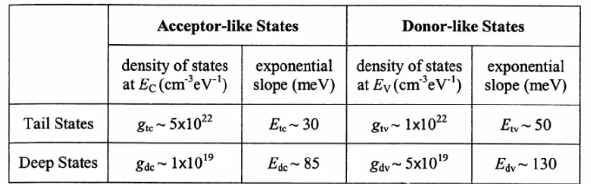
(11) Table Captions Chapter Two Table 2-1 Physical properties of a device-quality a-Si:H.. Chapter Three Table 3-1 Typical values of the parameters for the exponential model of. DOS for intrinsic a-Si:H Compiled from Ref. 10.. VII. the.
(12) Figure Captions Chapter One Figure. 1.1 The electron energy levels of silicon in different bonding states. Figure. 1.2 A schematic diagram of the electron density of states for an amorphous semiconductor, such as a-SiH. Figure. 1.3 Typical TFT transfer characteristic simulated under illumination. Figure. 1.4 TFT in the OFF-state (regime (III)) under illumination. Figure. 1.5 Figure 1.5 Simulated variations of the electron and hole Fermi potentials along the main TFT current path (the TFT being illuminated).. Chapter Two Figure. 2.1 Cross-sectional view of a BCE TFT where the SiNx gate insulator in this experiment.. Chapter Three Figure. 3.1 Microscope、Hot chuck、Probe station Figure. 3.2 Agilent B2201A (Switch) and Keithley 4200-SCS. Figure. 3.3 Temperature controller. Figure. 3.4 Agilent 4156C、Agilent E5250A (Switch) andAgilent 41501B (high power) Figure. 3.5 Illustration of the Cryogenics System (TTP-6 Probe Station) Figure. 3.6 Illustration of the density of states (DOS) in intrinsic a-Si:H.(After Shaw and Hack, Ref. 10. © 1988 AIP.) Figure. 3.7 Representative dependence of the activation energy vs.gate voltage dependence for the transistors with incorporated n+ contact layers.. VIII.
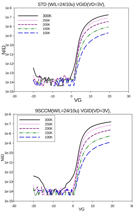
(13) Figure. 3.8 Density of states vs. activation energy. Chapter Four Figure. 4.1 The relationship between the Fermi level and the increase of. acceptor-like deep state Sketch Figure. 4.2 The ID-VD transfer characteristics of the SiF4-9sccm and a-Si TFT with temperature at 300K and 100K, individually.(a)300K, (b)100K Figure. 4.3 The ID-VG transfer characteristics of the SiF4-9sccm and a-Si TFT with temperature at 300K to 100K. Figure. 4.4 Shows the ON resistance of the SiF4-9sccm and a-Si:H TFT at low temperature Figure. 4.5 The △% of VT (△VT/VT300K) and carrier mobility(△μ/μ300K ) Figure. 4.6 The ID-VD transfer characteristics of the SiF4-9sccm and a-Si TFT with light illuminated by temperature at (a)300K and (b)100K, individually. Figure. 4.7 The transfer characteristics VG-ID in the linear regime of (a)the STD a-Si TFT devices and (b)the SiF4-9sccm a-Si TFT with light illuminated by temperature at 300K and 100K, individually. Figure. 4.8 At VG= -7V,-10V, -15V, change of Photo Leakage Current of the SiF4-9sccm a-Si TFT and the STD a-Si TFT. Figure. 4.9 Arrhenius plot of carrier and emission time for an individual interface trap. Figure. 4.10 Ionized charge concentration versus temperature for silicon. Figure. 4.11 The parasitical resistances of N+ from 100K to 300K. Figure. 4.12 The device was illuminated under two direction:(a) under front-side. illumination(Top-Light ) and(b)gate-side illumination(Bottom-Light). Figure. 4.13 The comparison of VG -ID characteristics between top light illuminated. IX.
(14) and bottom light illuminated. (a)STD (b)9sccm Figure. 4.14 The change of photo leakage current under high and low light illuminated Figure. 4.15 The comparison of VG -ID characteristics between top light illuminated and bottom light illuminated Figure. 4.16 Illustration of region for light illuminated and electron–hole pairst (a) Top light illuminated (b) Bottom light illuminated Figure. 4.17 ID-VG transfer characteristics of stress with (a)the STD a-Si TFT and (b)the SiF4-9sccm a-Si TFT, individually. Figure. 4.18 ID-VG transfer characteristics of the STD a-Si TFT .After and before stress with (a) Top light illuminated and (b) Bottom light illuminated, individually. Figure. 4.19 ID-VG transfer characteristics of the SiF4-9sccm a-Si TFT .After and before stress with (a) Top light illuminated and (b) Bottom light illuminated, individually. Figure. 4.20 After and before stress, (a)The activation energy – gate voltage (Ea -VG) and (b) Density of states characteristic of the STD a-Si TFT Figure. 4.21 After and before stress, (a)The activation energy – gate voltage (Ea -VG) and (b) Density of states characteristic of the SiF4-9sccm a-Si TFT Figure. 4.22 After and before stress, ID-VG transfer characteristics of the STD a-Si TFT and the SiF4-9sccm a-Si TFT with(a) no-light illuminated and (b) bottom light illuminated, individually.. X.
(15) Chapter One - Introduction 1.1 Introduction 1.1.1 Overview Thin-film transistors (TFTs) including an active layer of amorphous silicon or polycrystalline silicon have been widely employed as the pixel-driving elements of a liquid crystal display (LCD). a-Si:H TFT is particularly advantageous to the production of large screen displays and facilitates mass production.[1-1] When employing an a-Si:H layer, the main objectives are to enhance the field effect mobility and to reduce the off-state leakage current under light illumination. The increase of field effect mobility results in wide application of a-Si:H TFTs in high resolution LCDs. On the other hand, a-Si:H has high photoconductivity which results in high off-state leakage currents of a-Si:H TFT under light illumination.[1-2] The off-state leakage current under light illumination is, in particular, a serious problem in the projection and/or multimedia displays that require high intensity backlight illumination. Recently, the fully self-aligned a-Si:H TFT was developed to reduce the parasitic capacitance between source/drain and gate electrodes. However, it has high off-state leakage current under light illumination compared to conventional TFT.[1-3] Therefore, to reduce the off-state leakage current in a-Si:H TFT under illumination is very important to obtain a high quality TFT-LCD.. 1.1.2 Hydrogenated Amorphous Silicon Hydrogenated Amorphous Silicon (a-Si:H) first came to prominence as a. 1.
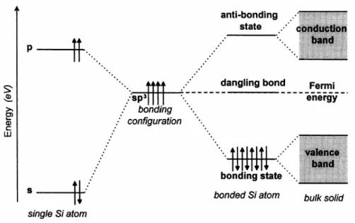
(16) potentially useful electronic material through the work of Spear and coworkers in the 1970s.[1-4] Since then, there has been significant research and development worldwide to bring a-Si:H to the current state in which it is routinely used in TFTs with a large switching ratio (<106) and a low off state current between the source and drain which is suitable for controlling AMLCDs.[1-5] A large body of research into this material has been required due to its complex nature. Although many of the properties of a-SI:H are reminiscent of crystalline silicon , the amorphous nature of the material has an effect upon the electron energy band structure and the carrier transport properties. The presence of hydrogen and dangling bonds inside the disordered structure further complicates the system.[1-6]. 1.1.3 Atomic Structure and the Electron Density of States Crystalline silicon (c-Si) has a well-defined tetrahedral lattice structure with a bond length (a) of 0.35 nm between adjacent atoms and a corresponding bond angle (θ) of 109°. In the case of a-Si:H, although the material has little or no long range atomic order, on short length scales (up to ~1 nm) the tetrahedral structure of the silicon network is preserved. The tetrahedral structure is a direct result of the electronic structure of the silicon atom, which has four valence electrons. When unbonded, two electrons exists in the 3s state and two in the 3p state. Fig. 1.1 shows this situation in terms of the energy of the electrons in each state.[1-7] In each state, one electron exists in “spin up” configuration and one in a ”spin down” configuration so as to satisfy the Pauli Exclusion Principle. However, such a configuration only allows two covalent bonds to be formed with neighboring silicon atoms. In order to maximize the. 2.
(17) number of bonds possible, the s and p electron states combine to form four sp3 states at an energy between the s and the p levels, and this permits bonding with up to four silicon atoms at the tetrahedral angles, as each bond is equivalent. This is shown as the bonding configuration in Fig. 1.1. When an sp3 orbital forms during bonding, a second electron is contributed to the state by the other atom, and interaction between the two electrons lowers the energy of the state. Therefore, the sp3 energy level splits into a bonding level, and an anti-bonding level (Fig. 1.1). In a real solid, there is a Coulomb interaction between the atom cores and electrons, and so the bonding and anti-bonding energy levels split forming a continuum of extended states, with the band of bonding states and the anti-bonding states being the conduction band. In the approach, the a-Si:H network is considered to consist of identical Si- Si bonds, as in c-Si.. In reality, the amorphous structure introduces a degree of disorder into the system so that there is a range of bond lengths (△a) and bond angles (△θ) around the crystalline case. For device quality a-Si:H, it is found that △a is about 2% of the crystalline bond length (a) while △θ is about 10% of the crystalline bond angle (θ). This leads to what is best described as a “continuous random network” of silicon atoms.[1-7] The bonding deviation in a-Si:H perturbs the energy of the bonding and anti-bonding states in a particular bond. Therefore, whereas the edges of the conduction and valence bands are well defined in c-Si, in the a-Si:H the band edges are smeared out, leading to the formation of localized “band tail” electron states which extend into the band gap, decreasing exponentially as shown in Fig. 1.2.[1-8] As the deviation in length and angle of a particular bond increase, the bond will become weaker and the perturbation of the electron energy levels will increase. Therefore, the band tails may be associated with the weakest bonds, the width of. 3.
(18) the band tails becomes a measure of the disorder in the network. The width of the tails is known as the Urbach energy (or Urbach slope)[1-8], and may be determined experimentally using either the constant photocurrent method (CPM) or photothermal deflection spectroscopy (PDS). It is not surprising that if a particular bond is highly deformed, then it becomes so weak that the breaking of the bond to form two “dangling bonds” (otherwise known as co-ordination defects) represents a lower energy. The energy of this state will be at the “bonding configuration” sp3 level shown in Fig. 1.1. A bond between two silicon atoms normally contains two electrons, and so, after breaking, each dangling bond will contain one electron. Each dangling bond has the potential to contain two electrons (one spin-up and one spin-down) and so is 50% occupied. The Fermi level is, by definition, the energy at which there is a 50% probability that an electron state is occupied. Therefore, the Fermi level must be at the dangling bond sp3 energy. The bonding and anti-bonding states do not split evenly around the sp3 energy (Fermi level), and in fact the conduction band is found to be slightly closer to the Fermi level than the valence band. This leads to the phenomenon, which is observed experimentally, that undoped a-Si:H is slightly n-type.[1-9] For comparison, undoped crystalline silicon, by definition, has no dangling bonds, and so the Fermi level lies exactly in the middle of the mobility gap, and so is genuinely intrinsic in nature.[1-6]. 4.
(19) 1.2 Photo leakage current mechanism[1-10] The numerical simulation program solves simultaneously the three equations describing the steady state conduction in semiconductors (Poisson equation, electron and hole continuity equations), out of thermal equilibrium, using the Shockley Read model for the carrier recombination rate. The amorphous silicon density-of-states is composed of two exponential band tails and two gaussian distributions of monovalent states, where the recombination process takes place. The program takes into account both the interface (a-Si / a-SiN and back channel interfaces) and the bulk state densities. The gate insulator is assumed to be idea, which means that there is no charge trapping or fixed charge present in the insulator layer. The TFT is illuminated from the source-drain side, and the original assume that the whole a-Si:H layer is exposed to the light. Fig. 1.3 is a transfer characteristic simulated under a uniform illumination. The analysis of the simulated results has shown that the original can distinguish both the TFT electron and hole threshold voltages, that delimit three main TFT operating regimes: (I) : electron accumulation layer created at the a-Si:H / a-SiN interface, (II) : no accumulation layer, (III) : hole accumulation layer created at the a-Si:H / a-SiN interface. In the regime (I), the TFT drain current is associated with the drift-diffusion of electrons in the accumulation layer (conduction channel). In the regime (II), the TFT drain current results from the same mechanism than in regime (I), but the conduction occurs uniformly in the whole amorphous. 5.
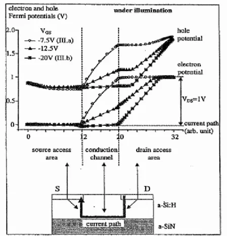
(20) silicon layer (channel and bulk), as there is no carrier accumulation at the amorphous silicon / silicon nitride interface. Because the carrier densities in the whole amorphous silicon layer depend mostly on the light-induced generation and carriers recombination rates, in this regime, the TFT drain current is sensitive to the amorphous silicon thickness and to the bulk density-of-states of amorphous silicon. In the regime (III), the existence of the hole accumulation layer at the a-Si:H / a-SiN interface in combination with the n+ a-Si:H source / drain contact layers, results in the creation of two PN junction located at the source and drain access areas. For a positive drain voltage, as the original have shown in Fig. 1.4, the source and drain junctions are respectively in the ON- and OFF-state. Within the regime (III), there are actually two different conduction regimes that depend on the relative importance of two different physical mechanisms. In regime (III.a), the drift-diffusion of hole in the accumulation layer (conduction channel) is predominant, whereas in regime (III.b) the recombination of electrons and holes in the drain (OFF-state) PN junction depletion region is the most important. The original have plotted Fig. 1.5 the simulated variations of the electron and hole Fermi potentials along the usual TFT current path between the source and drain contacts. We can see that, in the regime (III.a) (VG=-7.5V), the main variation of the Fermi potential happens in the accumulation layer, where the drift-diffusion of holes occurs. The conduction in this regime is similar to the conduction when the TFT is in accumulation regime (gate voltage larger than the electron threshold voltage); however, in this regime, the majority carriers are the holes instead of the electrons. On the contrary, in the regime (III.b) (VG=-20V), the main variation of the Fermi potentials occurs in the drain PN junction depletion region, where the recombination of electrons and holes is taking place. In this case, the TFT current 6.
(21) depends only on the light-induced generation and recombination of electrons and holes in the drain PN junction depletion region. Actually, for high negative voltages, the recombination rate can be neglected and the TFT current is therefore only set by the light-induced generation of electrons and holes (as in a photodiode case). In particular, in this regime, there is no longer any influence of the gate voltage (saturation phenomenon) or channel length on the TFT drain current. The parameters that influence the TFT drain current depend on the TFT operation regime to be considered. The analysis of the original simulated results has shown that: The electron and hole threshold voltages depend mostly on the amorphous silicon density-of-states associated with both the a-Si:H / a-SiN interface and with the bulk the difference between the two threshold voltages is higher for a larger density-of-states. In the regime (II), the TFT drain current depends strongly on the amorphous silicon thickness, but also on the a-Si:H bulk density-of-states: it increases with the a-Si:H thickness and decreases with the a-Si:H density-of-states. The drain current in the regime (III.b) depends only on the light-induced generation of electron-hole pairs in the drain PN junction depletion region (between the drain contact and the a-Si:H / a-SiN interface): it increases with the illumination intensity and with the PN junction area. The relative importance of the two main mechanisms involved in the TFTs electrical instabilities (modification of the a-Si:H density-of-states and charge trapping in the insulator layer) is not yet perfectly accepted. In general, the charge trapping in the insulator layer results in variations of both the electron and the hole threshold voltages in the same direction, while modifications of the amorphous silicon density-of-states results in variations of the threshold voltages in opposite direction. 7.
(22) More precisely, an increase in the bulk density-of-states will result mainly in a shift of the electron and hole threshold voltages toward more positive and negative gate voltages respectively, and in a reduction of the TFT drain current in the regime (II). The interface density-of-states will also affect the threshold voltages. But in the regime (II), the whole a-Si:H layer is involved in the conduction; therefore the influence of interface density-of-states on the drain current is not significant in comparison to the influence of bulk density-of-states.. 8.
(23) 1.3 Some solutions for reducing photo leakage current a-Si :H has high photoconductivity which results in a high off-state leakage current for an a-Si :H TFT under backlight illumination [1-2]. The off-state leakage current can be lowered by reducing the thickness of undoped a-Si:H, however, this also decreases the field effect mobility of the TFT.[1-11] The off-state leakage current of a-Si:H TFT is mainly due to holes induced at the a-Si:H interface to a gate insulator. However, under light illumination, electrons are the majority carriers when a negative gate voltage is applied to the TFT because electron mobility is much higher than that of hole.[1-12] The off-state leakage current of a-Si :H TFT under light illumination is related with its photoconductivity. The photoconductivity of a-Si : H(: Cl) is at least two orders of magnitude lower than that of undoped a-Si :H.[1-13] Recently, Cl incorporated hydrogenated amorphous silicon [a-Si:H(:Cl)] has been prepared by various deposition methods using SiH2Cl2 mixtures to improve film quality,[1-14] stability[1-15] or to increase deposition rate.[1-16]However, the performance of the a-Si : H(: Cl) TFTs was found to degrade with increasing [SiH2Cl2]/[SiH4] ratio which was used to deposit the a-Si : H(: Cl).[1-17] The a-Si:H(:Cl) films show p-type conduction, leading to lower photoconductivity. The off-state dark leakage current of a-Si:H(:Cl) TFTs is lower than that of a-Si:H TFTs, which is due to the position of the Fermi level of a-Si:H(:Cl). The Fermi level of a-Si:H(:Cl) that exists is lower than that of a-Si:H. But, with increasing [SiH2Cl2]/[SiH4], the field effect mobility decreases slightly and the threshold voltage increases. The increase in the threshold voltage may be due to the increase in the defect 9.
(24) density by Cl incorporation and/or due to the shift of the Fermi level in the band gap toward the valence band edge. The density of states in the gap of a-Si:H(:Cl) will be modified by the introduction of Cl into a-Si:H, resulting in the shift of the Fermi level toward the valence band edge. The Fermi level of a-Si:H is determined from the charge neutrality condition. The acceptor-like states are extended from the conduction band edge and the donor-like states from the valence band edge; dangling bonds exist around midgap. Of these, some states are charged positively and other states are negatively charged by the same amount. The position of the Fermi level can be lowered by a reduction of donor-like states or by an increase of acceptor-like states. The modification in the density of the states in the gap by the incorporation of Cl atoms in a-Si:H should be studied in the future in order to understand the origin of the shift of the Fermi level toward the valence band edge by Cl incorporation. The shift in the Fermi level leads to a reduction of the photoconductivity of a-Si:H(:Cl). The photoconductivity of a-Si:H is strongly related to the position of the Fermi level.[1-18] The off-state leakage current of an a-Si:H TFT under light illumination is related to its photoconductivity, so the photoconductivity for the a-Si:H(:Cl) films was investigated. The photoconductivity of a-Si:H(:Cl) is at least two orders of magnitude lower than that of intrinsic a-Si:H. The position of the Fermi level for a-Si:H(:Cl) film lies below the midgap, so that the a-Si:H(:Cl) shows p-type behavior. It should be noted that the photoconductivity of p-type a-Si:H is much lower than that of n-type a-Si:H because the mobility of electrons is much higher than that of holes.. 10.
(25) Chapter Two - Fabrication 2.1 Deposition of Hydrogenated Amorphous Silicon by PECVD The a-Si:H and SiNx utilized in TFT array fabrication are prepared by PECVD. The TFT performance depends on the preparation conditions, such as substrate temperature, RF power, and gas dilution. Oxygen incorporation during a-Si:H deposition in particular has been found to greatly degrade TFT performance, because it increases the defect density in the undoped a-Si:H. Hydrogenated amorphous silicon has a short-range order, which means that the coordination number, bond angle, and bond length are close to those for a single crystalline Si within 2 or 3 atomic distances, but there is no periodicity in the long range. Because of this there are a considerable number of localized states in the gap. The hydrogen in the a-Si:H reduces the dangling bonds by passivation. Therefore, the dangling bond density of ~1020 cm-3 in vacuum-evaporated a-Si or sputtered a-Si is reduced to 1015~1016 cm-3 in PECVD a-Si:H, where hydrogen content is 10-30 at. %. The hydrogen reduces the tail-state density in addition to the reduction of dangling bonds, because the disorder is decreased by hydrogen incorporation. Typically, undpoed a-Si:H for TFT applications is prepared at a substrate temperature of 220-350℃. The hydrogen in a-Si:H may be incorporated as SiH or SiH2 ; however, only films with hydrogen bonded as Si-H are suitable for TFT application.[2-1] Precursor gases for PECVD deposition of a-Si:H may be SiH4 or Si2H6, with H2 , He, and /or Ar being used as carriers/diluents to decrease the density of localized states or modify the material into μc-Si. The μc-Si is deposited by 11.
(26) PECVD under similar deposition conditions used for a-Si:H, except with high dilution of silane with hydrogen. The grain size is usually less than 50nm, and film shows a columnar growth. Because the grain size is quite small and there are a lot of defects inside the grains the field-effect mobility of μc-Si is comparable to that of high-quality a-Si:H TFTs. Moreover, the off-state drain current is much higher than that of a-Si:H TFT because of its high conductivity (>10-6 S/cm) and high density of defects. The hydrogen/silane dilution ratio is typically higher than 30 for the growth ofμc-Si, and the RF power is also an important parameter. The role of hydrogen during the deposition in the PECVD chamber can be summarized as follows: 1. Hydrogen atoms cover the growing surface and increase the diffusion length of the Si precursors. Therefore, the precursors can migrate to a more stable position.[2-2] 2. Atomic hydrogen diffuses into the silicon network down to a few nanometers and thus enhances the relaxation of Si atoms, leading to the more stable structure.[2-3] 3. Atomic hydrogen etches the weak Si-Si bonds and thus more stable Si-Si bonds are formed .[2-4] The precursor for a-Si:H deposition is SiH3.[2-5] Films of a-Si:H deposited by PECVD at lower RF power have better step coverage and low defect density, whereas a-Si films deposited at higher RF power generally have more defects. Particles can be formed by plasma polymerization of radicals and/or ions in the PECVD chamber. In addition, the plasma potential during deposition can cause ion damage of the growing film, which is especially a problem at high RF power .[2-6] Among the various deposition control variables, such as gas flow rate, gas pressure, RF power, and substrate temperature, the hydrogen content of the final. 12.
(27) film is greatly affected by the substrate temperature. The hydrogen content decreases with increasing substrate temperature because of the enhanced out-diffusion of hydrogen from the film. Therefore, the optical band gap decreases when increasing the substrate temperature, since the optical band gap increases with hydrogen content in the a-Si:H. The deposition rate increase with the gas flow rate, but at high flow rates there is more gas-phase, plasma polymerization. At too low a flow rate, more ion damage is expected because of the increased plasma potential. Therefore, an optimum intermediate flow rate is important for the deposition of device-quality a-Si:H. During a-Si:H deposition, the precursor arriving at the growing surface is mainly SiH3, and it bonds with the surface atoms, resulting in the deposition of a-Si:H and out-diffusion of hydrogen. The products can be H2 and /or SiH4. Deposition occurs by heterogeneous reaction at the growing surface[2-7], and ion bombardment of the surface can affect the film property. Increasing the RF power decreases the surface diffusion length of precursor radicals and increases the sticking coefficient to the substrate. Table 2.1 shows the physical properties of device-quality a-Si:H used for TFT fabrication.. 13.
(28) 2.2 Deposition of SiNx by PECVD Plasma-deposited silicon nitride, SiNx, is used for the passivation of electronic devices and as the gate insulator of choice for a-Si:H TFTs. As a passivation film, silicon nitride protects against the diffusion of water vapor, sodium, and oxygen into the active device. The hydrogen content of plasma-deposited silicon nitride is 10-40 at.%, and most of the hydrogen atoms are bonded as Si:H and/or N-H, depending on the preparation conditions, such as RF power, feeding gas, and substrate temperature. Total hydrogen content decreases with increasing substrate temperature or increasing RF power.[2-8] Silicon nitride has an amorphous structure, and properties depend on the relative atomic concentrations of silicon, nitrogen, and hydrogen. For good-electrical-quality a-Si:H TFTs, PECVD-deposited SiNx is much more suitable than stoichiometric Si3N4. Silicon nitride deposited at 300-350℃ (abbreviated as SiNx or SiN:H) is quite a different material from Si3N4 produced by CVD at 700-900℃.[2-9] Hydrogen in saturating the traps, so the defect density is much less than that of a CVD Si3N4. The interface charge density between a-Si:H and SiNx is typically in the range of 2×10¹¹ to 7×10¹² eV-1cm-2, and it strongly depends on the deposition conditions: it increases with decreasing substrate temperature or decreasing RF power. Note that the trap density in SiNx increases on heating above 400℃, because the hydrogen is out-diffused as a result of breakage of hydrogen bonds in Si-H and /or N-H modes.[2-10] The ability to form a good insulating film at low temperature (less than 350 ℃) having a low interface state density with a-Si:H (~1011 eV-1cm-2) makes SiNx a 14.
(29) good gate insulator. In addition, the ability to employ the same PECVD equipment used to deposit the a-Si:H is an important advantage. SiNx is typically deposited from a mixture of SiH4, NH3, N2, and He at 300-350℃. The RF power is typically higher than used for a-Si:H deposition, and the best material for the TFTs is a N-rich SiNx.[2-11] The field-effect mobility in the linear region is of prime importance for pixel charging in TFT-LCD application. The interface between SiNx and a-Si:H affects the field-effect mobility; in particular, the surface roughness of the SiNx layer is important because it affects the initial growth of a-Si:H, which forms the active channel layer for the TFT[2-12].. 15.
(30) 2.3 Deposition of n+ Hydrogenated Amorphous Silicon by PECVD Deposition of an n+-a-Si:H layer between undoped a-Si:H and a metal allows the formation of an ohmic contact between them. The ohmic contact also acts a hole-blocking layer because it acts to depress the position of the contacting semiconductor valence band with respect to the Fermi level of the metal. The resistivity of n+-a-Si:H is about 100Ω-cm, which is much higher than that of n+ crystalline silicon. Even though the resistivity is relatively high, the current is not generally limited by the n+ contact itself, because the drain current is on the order of microamps. For typical AMLCD TFT channel lengths (~10µm) and for thickness of a-Si:H below ~100nm, the use of n+ poly-Si or n+ µc-Si contact layers dose not appreciably increase the drain current over that of standard n+-a-Si:H contact. In most cases, n+-a-Si:H is deposited by PECVD using a silane mixture containing ~1% PH3. PECVD deposition using this doping gas mixture diluted at a ratio of ~1:50 in hydrogen allows the formation of n+ µc-Si. Adding more than ~1% PH3 to silane does not further decrease the resistivity of n+-a-Si:H, because the defect density of the material begins to grow in proportion to the added dopant, negating any further enhancement of the free carrier population.[2-13]. 16.
(31) 2.4 Process Flow Inverted-staggered a-Si:H TFTs with back-channel-etched (BCE) process, were fabricated on glass substrate for the study of electrical characteristics, where Al is used as source/drain metal as shown in Fig. 2.1. The device fabrication process was described as followed. After a 3000-Å-thick Cr gate electrode was patterned on the glass substrate, a 3000-Å-thick silicon-nitride (SiNx) layer, a 2000-Å-thick a-Si:H(:F) active layer and a 500-Å-thick n+- a-Si:H were continuously deposited by plasma enhanced chemical vapor deposition (PECVD) method. The undoped a-Si:H(:F) was deposited with a gas mixture of 9sccm SiF4 and 50 sccm SiH4 at 200 °C. The n+ -a-Si:H layer in the TFT channel region would to be etched off using the source/drain pattern as a mask, after the electrodes are formed for TFTs. In order to decrease the device degradation of a-Si:H(:F) layer, the a-Si:H/a-Si:H(:F) double channel layer structure was also fabricated for this study. The thickness of a-Si:H and a-Si:H(:F) in double layer structure were 40 nm and 160 nm respectively. The channel length of TFT devices varied from 5 to 16 µm and the channel width was kept constant 24 µm. Similarly, the conventional a-Si:H TFT without gas mixture of SiF4 were also fabricated as a reference sample. The characteristics of the amorphous Si TFTs demonstrated the filed-effect mobility ~0.1cm2/V-s, the minimum subthreshold swing ~ 1.08V/dec, the threshold voltage ~ 1.95V defined at constant current 10nA ,and the ION/IOFF ratio ~106 at VDS=10V. The leakage current through gate insulator is less than 10-13 A The photo leakage current measurement was carried by light illumination to compare the difference in the off- state photo leakage currents between the a-Si:H(:F) TFT and the conventional one.. 17.
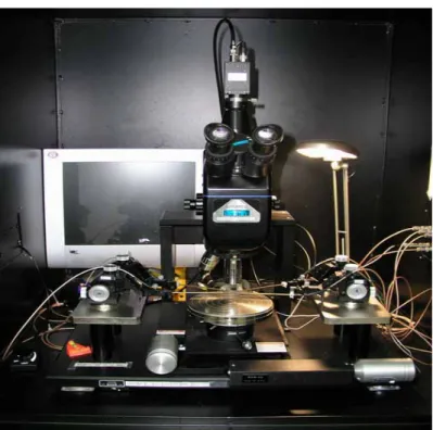
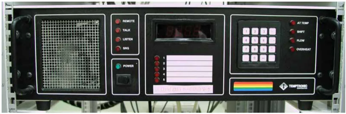
(32) Chapter Three - Apparatus and Parameters 3.1 Apparatus List 3.1.1 The room temperature and high temperature (1) Microscope、Hot chuck、Probe station, as shown in Fig. 3.1. (2) Agilent B2201A (Switch) and Keithley 4200-SCS , as shown in Fig. 3.2. (3) Temperature controller as shown in Fig. 3.3.. 3.1.2 The low temperature (1) Agilent 4284A、Agilent 4156C、Agilent E5250A (Switch) Agilent 41501B (high power), as shown in Fig. 3.4. (2) Cryogenics System-- TTP-6 Probe Station, Fig 3.5.. 3.1.3. Software of measurement. ICS(Interactive Characterization Software) Use the Software to get : 1. VD-ID 2. VG-ID (Linear Region VD=1V,3V) 3. VG-ID (Saturation Region VD=10V) 4. VG-Gm Note:. VD : Drain Voltage. ID : Drain current. VG : Gate Voltage. IG : Gate current. Gm : VG - ID max slope. 18.
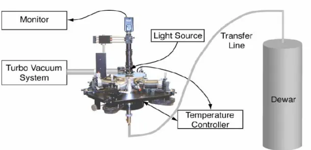
(33) 3.2 Setup instruments for Current-Voltage (I-V) Measurement. 3.2.1 The room temperature and high temperature The current – voltage characteristic measurement of thin film transistor devices was performed by 4200-SCS semiconductor parameter analyzer with source grounded and body floating. The electrical test setup of 4200-SCS semiconductor parameter analyzer, illustrated at Fig. 3.2, a probe station situated inside a dark box. The ground probe station is furnished with an electrically isolated, water-cooled thermal chuck. The chuck is controlled by TEMPTRONIC TPO315A thermal controller, which can operate temperature from 25 ℃ to 300oC. An Keithley 4200-SCS precision semiconductor parameter analyzer provides I-V measurement, bias for BTS. The 4200-SCS are connected to E5250A low leakage switch mainframe, and then link to dark box. The current-voltage (I-V) characteristics measurements were gotten by using p-TFT structure with Keithley 4200-SCS precision parameter analyzer. Keithley 4200-SCS can measure the minimum leakage current: 1f (A).. 3.2.2 The low temperature The system is illustrated in Fig. 3.5. The photo shows the TTP with the. 19.
(34) microscope and camera installed. The remaining components necessary to run the system are connected to the TTP. To use the system, samples are placed inside the TTP chamber, the system is evacuated with the turbo vacuum system, and the sample is cooled with a cryogen. Probes are moved into place on the sample while observing with the microscope. Measurements of sample properties are then made via the probes[3-1]. When the system is not used, the chamber needs to be kept the vacuum. We must vent the chamber with nitrogen gas to load a sample before measurement. After that, seal the chamber and evacuate it using turbo pump until the IG (ion gauge) readout on the vacuum system is 7.6E-5. Insert the both ends of the transfer line into a Dewar and the bayonet on the TTP, respectively, and set the desirable temperature on the temperature controller. Start to cool the sample down to the desirable lowest temperature and perform the experiment. We utilize microscope to view and make measurements of sample via the probes. Then, entering a set point on the temperature controller to warm the system, get back to the room temperature or even high temperature. After accomplishing the experiment, we must make the chamber temperature at room temperature before venting it. Finally, unload the sample and keep the chamber at vacuum state. The electrical test setup of HP4156C semiconductor parameter analyzer is utilized in this experiment, illustrated at Fig. 3.4. The same as 4200-SCS, the Agilent 4156C precision semiconductor parameter analyzer can provide I-V measurement, bias for BTS. We employ the ICS (Interactive Characterization Software) to obtain the output and transfer characteristics, like VD-ID, VG-ID (Linear), VG-ID (saturation), and extract the typical semiconductor parameters.. 20.
(35) 3.3 Method of Device Parameter Extraction In this section, we will introduce the methods of typical parameter extraction such as threshold voltage, subthreshold swing, field-effect mobility µFE, channel resistance and the parasitic resistance from device characteristics.. 3.3.1 Determination of the threshold voltage Plenty methods are used to determinate the threshold voltage which is the most important parameter of semiconductor devices. The method to determinate the threshold voltage in this thesis is the constant drain current method that the voltage at a specific drain current IN is taken as the threshold voltage. This technique is adopted in most studies of TFTs. It can give a threshold voltage close to that obtained by the complex linear extrapolation method. Typically, the threshold current IN = ID/( Weff / Leff ) is specified at 10nA for VD = -0.1V and 100nA for VD = -15V in most papers to extract the threshold voltage of. TFTs.. 3.3.2 Determination of the sub-threshold swing Subthreshold swing S.S (V/dec) is a typical parameter to describe the control ability of gate toward channel. It is defined as the amount of gate voltage required to increase/decrease drain current by one order of magnitude. The subthreshold swing should be independent of drain voltage and gate voltage. However, in reality,. 21.
(36) the subthreshold swing might increase with drain voltage due to short-channel effects such as charge sharing, avalanche multiplication, and punchthrough-like effect. The subthreshold swing is also related to gate voltage due to undesirable factors such as serial resistance and interface state. In this experiment, the subthreshold swing is defined as one-second of the gate voltage required to decrease the threshold current by two orders of magnitude. The threshold current is specified to be the drain current when the gate voltage is equal to the threshold voltage.[3-2]. 3.3.3 Determination of the field-effect mobility The field-effect mobility (µFE) is determined from the transconductance gm at low drain voltage. The transfer characteristics of a-Si TFTs are similar to those of conventional MOSFETs, so the first order I-V relation in the bulk Si MOSFETs can be applied to the a-Si TFTs, which can be expressed as I D = µ FE C ox. Where. W 1 2 [(VG − VFB )VD − VD ] L 2. (3-1). Cox is the gate oxide capacitance per unit area, W is channel width,. L is channel length,. VTH is the threshold voltage. If VD is much smaller than VG-VTH ( i.e. VD << VG-VTH ) and VG > VTH, the drain current can be approximated as: I D = µ FE C ox. W (VG − VFB )VD L. (3-2). The transconductance is defined as. 22.
(37) gm =. ∂I D ∂VG. VD = const .. =. WC ox µ FE VD L. (3-3). Therefore, the field-effect mobility can be obtained by µ FE =. L gm C ox WV D. (3-4). The mobility value was taken from eq. 3-4 with maximum µ FE .. 23.
(38) 3.3 Density of States 3.4.1 Overview The density of states (DOS) in the mobility gap of a-Si:H has been extensively studied using different experimental techniques such as field-effect measurement[3-3]-[3-4], measurements[3-5], (DLTS)[3-6].. In. transient. and addition,. and. deep-level other. steady-state. photoconductivity. transient-capacitance. methods. such. as. spectroscopy. capacitance-voltage. characteristics (C-V)[3-7], and dependence of capacitance on temperature and frequency. in. Schottky. diodes. and. metal-oxide-semiconductor. (MOS). structures[3-8] are also used for study of the DOS in a-Si:H. Based on these experimental studies, it is demonstrated[3-9]-[3-11] that the distribution of the localized states in a-Si:H mobility gap may be modeled by exponential distributions of deep and tail states for both acceptor-like and donor-like states (see Fig. 3.6). The localized states in the upper half of the mobility gap closer to the conduction band edge behave as acceptor-like states, while the states in the lower part of the gap closer to the valence band edge behave as donor -like states. Acceptor-like states are neutral when empty and negatively charged when filled with an electron, whereas donor-like states are positively charged when empty and neutral when filled with an electron. Based on this exponential DOS model, the density of the acceptor-like states gA(E) as a function of energy E may be written as follow:. 24.
(39) − ⎛ g (E ) = g exp ⎜⎜ E E ⎝ E A. tc. tc. C. ⎞ ⎟ + g exp dc ⎟ ⎠. ⎛ E − EC ⎞ ⎜ ⎟ ⎜ ⎟ ⎝ E dc ⎠. (3-5). where EC is the conduction band edge, gtc and gdc the densities of states at the conduction band edge for the tail and deep acceptor-like states, respectively, and Etc and Edc the associated slope of the exponential distribution of the tail and deep acceptor-like states, respectively. Similarly, the density of donor-like states gD(E) may be written as follows: ⎛E −E ⎞ ⎛E −E ⎞ ⎜ ⎟ ⎜ ⎟ ( ) = + g E g exp ⎜ ⎟ g exp ⎜ ⎟ V. D. tv. ⎝. E. V. tv. ⎠. dv. ⎝. E. dv. ⎠. (3-6). where EV is the valence band edge, and parameters gtv, gdv, Etv, and Edv are similarly defined for the exponential distribution of the tail and deep donor-like states. Typical values of these parameters for intrinsic a-Si:H are presented in Table 3.1. As can be seen from Fig. 3.6, the DOS is asymetrical in a-Si:H, i.e., the number of donor-like states in the mobility gap is higher than the number of acceptor-like states. As a result, following the neutrality condition, the position of the Fermi energy in an intrinsic a-Si:H sample in the dark (Ei) is closer to the conduction band edge. The position of the intrinsic Fermi energy is ~ 600 mV beneath the conduction band edge and is dependent on the temperature due to the asymmetrical DOS distribution[3-2][3-12].. 3.3.2. Evaluation of the density of states --Activation energy method[3-13]. As it was already mentioned, the Fermi level shift with the gate voltage is strongly dependent on the density of states (DOS). At high density of states more carriers must be induced in order to fill the states from EF upward and it is necessary to apply higher gate voltage in order to induce more carriers in the 25.
(40) channel. On the contrary, when the density of states is low, the states from EF upward are easily filled at low concentration of the induced charge and the Fermi level is easily shifted at low gate voltages. This correlation between the DOS and the gate voltage allows to obtain the shape of the density of states by studying the dependence of Eact vs. VGS. The information on DOS shape is important for understanding the physical mechanisms responsible for the device behaviour. The DOS shape is related to the threshold voltage value, subthreshold slope, field effect mobility and the stability of the TFTs. Globus et al. [3-14] proposed a method for evaluation of DOS in a-Si:H TFTs, from the dependence of Eact vs. VGS. If it is assumed that the DOS does not suffer sharp changes for energy interval about kBT, the charge of acceptor-like states Qt, filled by the gate bias is given by (3-7) where q is the electronic charge, Vs is the surface potential, EFo is the equilibrium Fermi level in the silicon layer g(E) is the density of states. The charge Qt can also be expressed as (3-8) where qnt is the surface charge, VFB is the flat-band voltage, εi and di are the gate dielectric permitivity and gate dielectric thickness, respectively, and dt is the thickness of the space-charge layer. Per measuring the drain-source voltage at different temperatures and keeping the same drain-source current, the activation energy (i.e. the Fermi level position) can be determined from the slope of the Arrhenius plot (log(IDS) vs. 1000/T) by the following equation:[3-15]. 26.
(41) (3-9) From eqs. (3.7) and (3.9), differentiating with respect to VGS, can be obtained (3-10) where Eact = EC -EFo - qVs is the activation energy, EF = EFo - qVs is the quasi Fermi level. Hence, the density of localized states can be related to the derivative of the activation energy with respect to gate bias:. (3-11). If it is assumed that the band bending in the a-Si layer is small compared to the characteristic energy of the density of states variation, then dt ≈ t where t is the a-Si layer thickness, and eq. (3.10) reduces to (3-12). This method for determination of the density of states is explained in details in [3-14]. According to ref. [3-14] this technique only accounts for the acceptor-like states in the bandgap. Advantage of the method is its simplicity. It is necessary to perform only field-effect measurements at different temperatures. Using this method, the density of states can be evaluated in relatively large energy interval from the bandgap. It is suitable for evaluation of changes in the density of states due to bias stress. Eq. (3.12) was employed to calculate the density of states in the complete. 27.
(42) devices (with incorporated n+ layer) according to the above-mentioned assumptions. As the measurements of Eact in the simplified sample are affected by the absence of n+ contact layer, we have not performed analysis of DOS for this sample. From the experimentally measured activation energy, depicted in Fig.3.7, we estimated the density of localised acceptor-like states in the upper part of the bandgap - in the interval 0.34 to 0.15 eV below EC. The calculated density of states, in energy interval 0.15-0.33 eV, is presented in Fig.3.8. The peak of the deep bandgap states can be observed at 0.34 eV. The Fermi level is pinned in these deep states when the TFT is in off-state. From 0.30 to 0.20 eV the shape of the acceptor-like states is nearly constant 17. -3. -1. about 5⋅10 cm eV . The Fermi level is shifted through these states in the subthreshold region of operation of the TFT. From 0.20 eV begins the exponential increasing of the acceptor-like tail states. The Fermi level is pinned at 0.15 eV from EC when the TFT enters in the on-state. This shape of the DOS is very similar to the obtained for the amorphous 17. silicon TFTs by Globus et al. [3-14]. In addition, the calculated value of 5⋅10 -3. -1. cm eV for 0.30 to 0.20 eV is slightly lower than the value of the maximal density 18. -3. -1. of deep bulk states (Nbs)max = 3.6⋅10 cm eV estimated from the subthreshold slope. This is because (Nbs)max was calculated assuming (Nss)max =0 The activation energy method is fast and simple and is suitable to observe the changes in the density of states due to bias stress, illumination, etc. The main disadvantage of this method and also of the method of the subthreshold slope is that they do not permit the separation of the bulk states from the interface sates at the channel/gate insulator. Both methods are based on field-effect measurements. 28.
(43) that are strongly dependent on the quality of the interface between the channel material and the gate insulator. This does not permit the exact evaluation of the intrinsic DOS of the channel material (in our case nc-Si:H), independently from the properties of this interface.. 29.
(44) Chapter Four. Experiments Results and Discussion. 4.1 Overview of the experiments sample 4.1.1 Characteristics Because a-Si:H is a photo-sensitive material, the main objectives for flat panel display application are to enhance the field effect mobility and to reduce the off-state leakage current under light illumination.[4-1] However, the higher off-state leakage current under light illumination compared to a conventional TFT has been observed.[4-2] As a result, the reduction of off-state photo leakage current in a-Si:H TFT is very important for TFT-LCDs technology. The thin-film transistor using a fluorine incorporated amorphous silicon [a-Si:H(:F)] and amorphous silicon (a-Si:H) stacked active layer, in which conduction channel is formed in a-Si:H and a-Si:H(:F). The a-Si:H(:F) TFT with backlight illumination the threshold voltage decrease and field-effect mobility increase slightly. The threshold voltage decrease result in the on current increase. With increasing [SiF4] / [SiH4] ratio, the field-effect mobility decreases and the threshold voltage increases. The increase in the threshold voltage may be due to the increase in the defect density by F incorporation and the shift of Fermi level in the band gap toward the valence band edge.[4-3] The photoconductivity of a-Si:H is related to the position of the Fermi level, so the shift in the Fermi level leads to a reduction of the photoconductivity[4-4]. The a-Si:H(:F) TFT with F incorporation has shown the larger threshold voltage and lower field mobility than conventional counterpart. In the a-Si:H(:F) channel the density of the donor-like defect states is reduced than the density of the acceptor-like defect states[4-5]-[4-6].Also, the a-Si:H(:F) TFT behaves as a similar p-type property compared with the a-Si:H TFT, and results in the little electrical 30.
(45) degradation with F incorporation. The correlation between the DOS and the gate voltage allows obtaining the distribution of the density of states by studying the dependence of Ea vs. VG. Globus et al.[4-7] The Fermi level is shifted through these states during the operation of TFT devices in the subthreshold region. The additional deep states have been found in the a-Si:H(:F) TFT .These additional deep states in a-Si:H(:F) TFT thereby resulted in lower photo leakage current compared to the a-Si:H TFT, and illustrated by the inset of Fig. 4.1. The increase of acceptor-like deep state in a-Si:H(:F) material leads to slightly electrical degradation on a-Si:H(:F) TFT, and results in the shift down of Fermi level.[4-1] Therefore, increasing [SiF4] / [SiH4] ratio, the acceptor-like states increase to make more recombination centers for electrons and holes. More recombination centers for electrons and holes can increase the carriers’ recombination rate, so the photo leakage current decreases The photo leakage current also related to its photoconductivity. The acceptor-like states increase causes the position of the Fermi level for a-Si:H(:F) film lies below the midgap, so that the a-Si:H(:F) shows p-type behavior. Due to these two important factor, the photo leakage current decreases.. 4.1.2. Relative parameters. After a complete TFT manufacture process, the characteristics of the undoped amorphous Si TFTs(a-Si:H) demonstrated the field-effect mobility form 0.43 cm2/V-s to 0.6 cm2/V-s, the minimum subthreshold swing from 0.58 V/dec to 0.59 V/dec, the threshold voltage was distributed from 1.9 V to 2.6 V determined from turn-on current (Ion) extrapolation in the linear region of ID-VG curve at. 31.
(46) VD=0.1V. ,and the ION/IOFF ratio~107 at VDS=10V. Besides, The 9sccm-SiF4 a-Si:H(F) TFT demonstrated the filed-effect mobility from 0.3 cm2/V-s to 0.58 cm2/V-s, the minimum subthreshold swing from 0.65 V/dec to 0.67V/dec, the threshold voltage from 3.8 V to 5.5V. With increasing [SiF4] ratio, the field effect mobility decreases, threshold voltage increases, and on current decreases. Leakage current of both through gate insulator is less than 10-13 A.. 32.
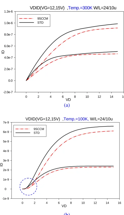
(47) 4.2 Characteristics at Low Temperature. 4.2.1 Motivation and experiment steps After a complete TFT manufacture process, In order to verify Electrical characteristics and photo leakage current variation at low temperature, it’s to perform the measurement of light illuminated and no-light illuminated at lower temperature for the STD a-Si TFT and the SiF4-9sccm a-Si TFT. In this experiment, we have two kinds of sample: 1. Standard TFT with active layer a-Si:H 2. SiF4(9sccm) TFT with active layer a-Si:H(:F) The experimental procedure is depicted below: Load the samples to the cryogenics system and cool the sample down to the desirable measurement temperature. Measure the I-V characteristics using the HP4156C semiconductor parameter analyzer. We measure I-V characteristics at 100K, 120K, 150K, 180K, 200K, 220K, 250K, 280K and 300K. And observe the difference between light illuminated and no-light illuminated. Then, we determine the all semiconductor parameters from the transfer characteristics.. 4.2.2 The electrical characteristics at low temperature Fig. 4.2 shows the VD-ID transfer characteristics curve at 100K and 300K, it’s detected current crowding effect at lower temperature. Normally, the effect of parasitic resistance can be clearly observed in the output characteristics of a-Si:H 33.
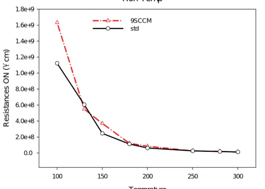
(48) TFT. The large parasitic resistance would lead to current crowding effect. Under operated at small drain voltages and high gate voltages, The TFT ON resistance, Ron, consists of the channel resistance Rch and the parasitic resistance R. parasitic.. The. contact resistance is also estimated with the following equations: Ron=Rch +R parasitic. (4-1). Rch=L/Wµ Ci(VG-VTH). (4-2). Where Ci is the gate nitride capacitance per unit area and W, L, and VTH are the intrinsic device channel width, length, and the threshold voltage, respectively.[4-8] Fig. 4.4 shows the ON resistance of the SiF4-9sccm and a-Si:H TFT at low temperature. During temperature decreasing, electrons activation of junction also get down and increase R parasitic. Due to the parasitic resistance increasing, the TFT should be drived by higher drain voltages. From 300K to 100K, it’s detected current crowding effect of VD-ID transfer characteristics curve at low temperature. In case of current crowding effect, it’s supposed to set VD=3V for the proper electrical characteristics data during VD-ID transfer characteristics curve measurement to avoid current crowding effect area. Fig. 4.3 shows VG-ID transfer characteristics curves of the STD a-Si:H TFT and the SiF4-9sccm a-Si:H(:F) TFT. There are two elements to change ID current: threshold voltage (VTH) and field-effect mobility ( µ FE ). We can derive the decreasing current at low temperature from the conducting current formula: I D = µ FE C. W 1 2 [(VG − VTH )VD − VD ] L 2. (4-3). When the temperature cooling the series resistance at R parasitic of the source and drain, will enlarge and lead the devices need the larger threshold voltage to turn on the TFT.. 34.
(49) Fig. 4.5 shows VT shift percentage (△VT/VT300K) and carrier mobility shift percentage(△µ/µ300K ). Comparing the SiF4-9sccm a-Si TFT and the STD a-Si TFT, the mobility is decreasing along with the temperature getting down, As sample’s mobility decreasing ratio of both is very similar, it presents carrier mobility decreases along with the parasitic resistance increasing. However, it’s opposite of threshold voltage shift percentage: Threshold voltage increasing ratio of the SiF4-9sccm a-Si TFT at low temperature is higher than that of the a-Si:H TFT, because the a-Si:H(:F) TFT behaves as a similar p-type property compared with the a-Si:H TFT, mobility and threshold voltage are worse. By formula(4-2), it’s estimated channel resistance1 is increasing more than temperature decreasing and threshold voltage shift ratio is higher.. 4.2.3 Measured with light illuminated at low temperature Due to the increase of contact resistance, current crowding effect is obvious at low temperature. However, under light illumination, the current crowding phenomenon is suppressed by the additional photo current. Fig. 4.6 Shows The ID-VD transfer characteristics of the SiF4-9sccm and a-Si TFT with light illuminated by temperature at 300K and 100K, individually. Fig. 4.7 shows the transfer characteristics VG-ID in the linear regime of the SiF4-9sccm a-Si TFTs and the STD a-Si TFT devices with bottom light illuminated by different temperature, respectively. On current of TFT under light illuminated is decreasing along with the temperature descending same as on current of. TFT. under no-illuminated; Nevertheless, it’s opposite of off current. Photo leakage current is increasing along with the temperature descending at 250K~150K but. 35.
(50) photo leakage current is decreasing at 100K. In order to understand the relation of photo leakage current along with temperature variation, to measure the SiF4-9sccm a-Si TFTs and the STD a-Si TFTs photo leakage current variation (△ID/ID) at different temperature in VG=-7V, -10V, -15V, as show in Fig. 4.8. To treat Photo Leakage Current variation into 2 parts:. ( I ) photo-leakage-current increasing along with the temperature descending Recombination mechanism is mainly indirect recombination to cause capture and emission through recombination centers. Capture time and emission time increasing along with the temperature descending. Thus, recombination rate becomes worse but photo leakage current becoming higher. Fig. 4.9 shows capture time and emission time to temperature, per 2 equations below: Capture time( τ C ) is estimated with the following equations:[4-9]. I(T)T 2τ C = ( 1 / σ 0α ) exp[( ∆EB / kT )] Where α = l(3 k/m*). 1/ 2. (4-4). /qµ0Vdω t ;l, w, and t are the channel length, width, and. thickness, respectively. σ 0 and ∆EB are the cross section prefactor and capture activation energy. Emission time( τ E ) is estimated with the following equations:[4-9]. T 2τ E = ( 1 / gσ 0 β ) exp[( ∆EB + ∆ECT ) / kT ] Where. β = A(3 k/m*)1 / 2 ;. (4-5). and ∆ECT is the trap binding energy.. ( II )Photo Leakage Current decreasing along with temperature drops to 200K According to the Seto’s model, the electrons activated from the doped atoms. 36.
(51) were filled at the trap states at the grain boundaries. For simplify, the amount of free carrier in N+ layers, Nfree, can be equated to: +. N free = N D − N T. (4-6). where ND+ is the number of ionized impurities and NT is the effective trap density. Thus, the conductivity is proportional to the amount of free carriers.[4-8] With the decreasing of the temperature, the amounts of activated electrons are decreasing and the ratio of trapped electrons is rising by assuming that the amount of trap states is non-varied. Ionized charge concentration versus temperature for silicon, shown in Fig. 4.10.[4-10] At temperature lower than 200K, the ionization is changing from Complete ionization to Partial ionization. The N+ resistance increasing to cause drain-source voltage decreasing in channel so the measured photo leakage current is lower. The parasitical resistances of N+ from 100K to 300K, are show in Fig. 4.11.[4-8] It’s obviously observed resistance increase slope becoming higher. That’s definitely Photo Leakage Current decreasing because of the N+ sheet resistance increasing. the N+ dopant could not fully activated resulting in the N+ resistance increasing. Comparing with the SiF4-9sccm a-Si:H(:F) TFTs and the STD a-Si TFTs photo leakage current, photo leakage current increase and decrease trends are the same at low temperature. But photo leakage current of a-Si:H(:F) TFT increase and decrease ration smaller is due to the recombination centers of a-Si:H(:F) TFT are more than that of a-Si:H TFT.. 4.2.4 Summary A-Si TFTs works as a larger resistor at low temperature than that at room temperature. As the mobility becoming lower, Turn-on current of TFT devices. 37.
(52) must be higher and threshold voltage shifts rightwards and on current decreasing. Besides, for the SiF4-9sccm a-Si TFT compared with the a-Si:H TFT similar to the p-type property and with lower mobility compared with the a-Si:H TFT, The threshold voltage increasing ratio is higher at lower temperature. Furthermore, more electron-hole pairs produced cause current crowding effect descending by current gain. But indirect recombination rate at low temperature is worse that that at room temperature. Under light illuminated, photo leakage current is also increasing along with the temperature descending. As temperature drops to 200K, the N+ dopant could not fully activated resulting in the N+ resistance increasing. Thus, the photo-leakage-current decreases. These results can provide the designers to consider the temperature effects for the a-Si TFT application in a suitable temperature range.. 38.
(53) 4.3 Light Illuminated Experiment. 4.3.1 Motivation and experiment Steps Because of equipment limitation, only top-light illuminated experiment at lowe temperature is performed. It’s to distinguish the difference of photo leakage current between top-light and bottom-light illuminated. To investigate electrical characteristics under top-light and bottom-light illuminated at room temperature. We have two types TFTs with different [SiF4] / [ SiH4] ratio: (1) Standard TFT with active layer a-Si:H (2) SiF4(9sccm) TFT with active layer a-Si:H(:F) Fig. 4.12 shows the device was illuminated under two direction : (a). under. front-side. illumination(Bottom-Light).. illumination(Top-Light) The. fluorine. and. incorporated. (b) amorphous. gate-side silicon. [a-Si:H(:F)] and amorphous silicon (a-Si:H) were illuminated with top-light and bottom-light. The backlight module’s light intensity was 3500 nits.. 4.3.2 A discussion on experiment results Fig. 4.13 shows the comparison of VG-ID characteristics between top light illuminated and bottom light illuminated, (a)STD (b)9sccm. When the light illuminated the threshold voltage decreases and field-effect mobility increases slightly. The decrease in the threshold voltage is due to the TFT. 39.
(54) active layer illuminated by light, causes a large number of electron–hole pairs created to lead the shift of the Fermi level in the band gap toward the conduction bang edge. The Fermi level in the band gap toward the conduction bang edge lead the threshold voltage decreases and the transistor turn on more easily. For photo leakage current under top-light illuminated, is much higher than that under bottom-light illuminated of inverted-staggered a-Si:H TFT. Top-light illuminate directly into channel but bottom-light illuminated the PN junction of source & drain due to light covered by gate metal layer under bottom-light illuminated. Fig. 4.14 shows VG-ID transfer curves of STD and SiF4-9sccm a-Si TFTs under the different light illuminated intensity;On current does not increase along with light illuminated intensity is raising, due to turn on operation of TFT devices located at Saturation area. But off current is increasing along with light illuminated intensity raising. As S.S variation as Vg= -5V~ 0V, photo leakage current by Vg= -20V~ -5V is increasing along with light illuminated intensity raising and VG-ID transfer curve is vertically lifted. On the other hand, VG-ID transfer curve is vertically falling down by light illuminated intensity descending and it’s helpful to compare with the VG-ID transfer curve measured of bottom light illuminated and top light illuminated. To adjust light illuminated intensity and have photo leakage current value of top light illuminated is closed to bottom light illuminated. The comparison of VG-ID characteristics between top light illuminated and bottom light illuminated show at Fig. 4.15. As Vg<-10V, it’s detected the different current transfer characteristics: Bottom light illuminated:As Vg<-10V, photo leakage current is increased, and, photo leakage current of SiF4-9sccm a-Si TFT is higher than that of the STD a-Si. 40.
(55) TFT. But, current transfer characteristics as Vg>-10V is opposite of that. The off-state dark leakage current of a-Si:H TFT mainly originates from the photo-induced hole current at the interface between a-Si:H and gate SiN layers. In contrast, electrons are the majority carriers of off-state current for the a-Si:H TFT under light illumination, since electron mobility is much higher than that of hole. [4-3] Due to higher vertical electrical field at source and drain separated the electron-hole pairs in channel and hole current occurring, photo leakage current is increasing along with gate bias raising.[4-10] Also, due to the SiF4-9sccm a-Si TFT increase in the defect density by F incorporation and due to shift of the Fermi level in the band gap toward the valence band edge[4-11]. Photo Leakage Current of the SiF4-9sccm a-Si TFTs is higher than that of STD a-Si TFTs shown in Fig. 4.16(b). Under bottom illumination, photo-leakage-current of the a-Si(:F) TFT is higher than STD TFT at larger negative gate votage(-15V~-20V) due to the hole accumulation. Top light illuminated : By way of ID-VG transfer characteristics measured, photo leakage current not increasing as Vg<-10V is mainly due to no vertical electrical field as electron-hole pairs produced by light illuminated in channel. As hole attracted as VG<-10V, electron is recombined with hole by state shown as Fig. 4.16(a). For the SiF4-9sccm a-Si TFT, due to shift of the Fermi level in the band gap toward the valence band edge[4-12]. Thus, current is slightly increasing along with gate bias raising but the whole ID-VG transfer characteristics is not effected. Current value, device width, active layer, DOS is related with light illuminated intensity.. 41.
(56) 4.3.3 Summary The off-state photo leakage current of a-Si:H(:F) TFT is smaller than those of conventional a-Si:H TFT in the density of states (DOS) limited region. It’s also because the a-Si:H TFT under back light illumination was in the non-equilibrium state( pn>ni^2). As a result, the trap states played the role of recombination centers. As VG= -5V~-20V, off-state current transfer curve up and down along with light illuminated intensity raising or descending but the trend shifts horizontally due to the off-state photo leakage current conducted by electron–hole pairs produced during light illuminated. The off current just raised without any leakage behavior change. The photo leakage current of a-Si:H(:F) TFT operated in the small negative gate voltage (VG>-10 V) and 1V drain voltage is less than conventional a-Si:H TFTs. Because the electric field is not large enough to separate the photo induced electron-hole pairs, the increased density of states serving as recombination centers in a-Si:H(:F) channel material has resulted in the lower photo leakage current. However, with the hole conduction region (VG<-10 V), the larger photo leakage current was observed. According to previous study,[4-6] The larger off-state photo leakage current is due to the faster hole channel accumulation in the larger negative gate voltage. The smaller hole accumulated voltage also indicated that the undoped a-Si:H(:F) shows near p-type-like behavior. There is no high electrical field to separate the electron-hole pairs and the hole conduction region is as VG<-10 V. Thus, photo leakage current is not increasing. In other words, photo leakage current under top light illuminated is not caused by the hole conducted as gate bias raising 42.
(57) Typical a-Si:H is n-type material even though the Fermi level lies near the midgap of undoped a-Si:H because the electron mobility is at least 10 times higher than that of hole.[4-4] The undoped a-Si:H(:F) TFTs have shown larger threshold voltage and smaller field effect mobility.. 43.
(58) 4.4 Reliability Experiment—DC Stress 4.4.1 Motivation and experiment steps TFT device is the pixel on/off switch of flat display and long-time operated by bias. The life time of TFT devices is very important. In order to know the SiF4-9sccm a-Si TFTs under the long-time operation, the reliability experiment is performed. Mainly, DC stress in channel to measure the electrical characteristics of the SiF4-9sccm. a-Si. TFTs. and. the. STD. a-Si. TFT. before. and. after. BTS(bias-temperature stress) and to observe the effect of photo leakage current under stress Stress voltage, VG=15V,VD=8V,VS to GND. Stress time, 800 sec. To measure the electrical characteristics once per Stress forced and sampling Ea and DOS at 0S, 800S, 1600S, and 2400S.. 4.4.2 A discussion on experiment results ID-VG transfer characteristics of stress with (a)the STD a-Si TFT and (b)the SiF4-9sccm a-Si TFT, individually shown in Fig. 4.17. Threshold voltage shift rightwards is due to carriers shock a-Si during the long time and strained bond broken to form Dangling Bond cause the defect density. Stress effect at 2400 sec. similar with that at 1600 sec, due to stronger bond remained after strained bond broken. Fig. 4.18~ Fig. 4.19 show ID-VG curve of the STD a-Si TFT and the. 44.
數據
+7

相關文件
• Conceptually there is a 4 x 4 homogeneous coordinate matrix, the current transformation matrix (CTM) that is part of the state and is applied to all vertices that pass down
Put the current record with the “smaller” key field value in OutputFile if (that current record is the last record in its corresponding input file) :. Declare that input file to be
To reduce the leakage current related higher power consumption in highly integrated circuit and overcome the physical thickness limitation of silicon dioxide, the conventional SiO
To reduce the leakage current related higher power consumption in highly integrated circuit and overcome the physical thickness limitation of silicon dioxide, the conventional SiO 2
Workshop of Recent developments in QCD and Quantum field theories, 2017
Schematic phase diagram of high-Tc superconductors showing hole doping right side and electron doping left side.. The common Features in
In section29-8,we saw that if we put a closed conducting loop in a B and then send current through the loop, forces due to the magnetic field create a torque to turn the loopÆ
雙極性接面電晶體(bipolar junction transistor, BJT) 場效電晶體(field effect transistor, FET).
