Low Leakage Current GaN MIS-HEMT with SiNx Gate Insulator using N2 Plasma
Treatment
S. C. Liua, H. C. Wanga, and E. Y. Changa
a
Department of Materials Science and Engineering, National Chiao-Tung University, Hsinchu, 300 Taiwan.
In this work, an effective N2 plasma treatment for suppressing
leakage current in GaN MIS-HEMT has been demonstrated. We observed an important issue of leakage current from the SiNx/GaN
interface. To investigate the leakage current mechanisms, we measured the leakage current from all the possible paths in the device structure, such as gate, mesa isolation, and drain leakage. The current−voltage measurement results reveal a severe leakage path at the SiNx/GaN interface after SiNx deposited on the GaN
surface without N2 plasma treatment. By using N2 plasma
treatment, we succeed in suppressing the leakage current and effectively improve breakdown voltage. A significant performance improvement of GaN MIS-HEMT with very low leakage current has been achieved through the N2 plasma treatment.
Introduction
Gallium nitride (GaN)-based High Electron Mobility Transistor (HEMT) with high breakdown voltage for high power switching applications are studied extensively in recent year. However, GaN HEMTs often suffer from surface state effects such as high gate leakage, current collapse, and a variety of reliability issues (1). Different materials such as SiNx (2), SiOx (3), and Al2O3 (4) were widely used as the gate dielectric and/or
passivation layer on AlGaN/GaN metal-insulator-semiconductor HEMTs (MIS-HEMTs). However, the Ga−O and Al−O bonds would easily form between oxide-based dielectric and AlGaN/GaN interface. The deep interface states could induce the current collapse severely under high gate or high drain voltages. Plasma-enhanced chemical vapor deposition (PECVD)-grown SiNx has been proved as an effective material to reduce the
surface states and can efficiently suppress current collapse in AlGaN/GaN HEMTs. However, the increase of surface leakage current from gate to drain and from the isolation etching area have been observed after SiNx deposition (5), (6). In this work, the
GaN MIS-HEMTs with very low leakage current by N2 plasma treatment are
demonstrated.
Devices Fabrication
The AlGaN/GaN heterostructure is grown by commercial metal-organic chemical vapor deposition (MOCVD) on silicon substrate. The mesa isolation was etched by inductively coupled plasma (ICP). Ohmic contacts were formed by an alloyed Ti/Al/Ni/Au metal stack. The gate metal was Ni/Au. For the high-power devices design in this study, the gate-to-drain spacing, the gate-to-source spacing, and the gate length are 15, 3, and 2 µm, respectively. The samples were treated by PECVD N2 plasma. The 20 nm SiNx was
deposited by PECVD as the gate dielectric. Three samples were separated after mesa and
10.1149/05302.0061ecst ©The Electrochemical Society ECS Transactions, 53 (2) 61-63 (2013)
61
) unless CC License in place (see abstract).
ecsdl.org/site/terms_use
address. Redistribution subject to ECS terms of use (see
140.113.38.11
ohmic contact were formed. The surface conditions before SiNx deposition were
prepared: sample A with N2 plasma treatment, sample B without treatment, sample C is
conventional HEMT sample without SiNx gate dielectric for comparing the leakage
current induced by SiNx deposition.
Results and Discussion
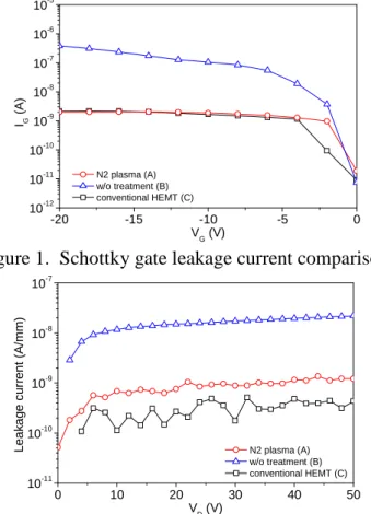
To investigate the leakage phenomenon, we measured the leakage current from any possible path in the structure, such as Schottky gate, isolation, and drain leakage current. Fig. 1 shows the GaN HEMTs IG−VG characteristics. In this work, the Schottky gate
leakage current of sample A is about three orders lower than sample B. It shows the gate leakage current of sample B increases easily when the gate bias voltages was applied. Fig. 2 shows the leakage current from mesa isolation region. The obvious increase of leakage current is observed after SiNx deposition. It indicates the SiNx thin film deposition will
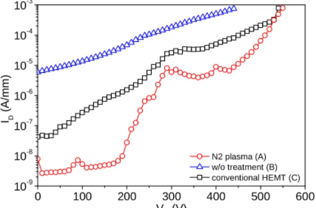
result in the increase leakage current from the mesa isolation region. This unwanted leakage current seriously affects the device performance when GaN HEMTs were operated at high bias voltage. Fig. 3 shows the OFF-state breakdown voltage characteristics. Under VD = 200 V, the leakage current of sample B is three orders higher
than sample A and the leakage current of sample A is extremely low in this study compared to the other samples. It reveals that the drain leakage current is effectively suppressed by N2 plasma treatment. This leakage current phenomenon reveals an
unfavorable GaN surface condition before SiNx deposition which will severely affect
devices performance. -20 -15 -10 -5 0 10-12 10-11 10-10 10-9 10-8 10-7 10-6 10-5 IG ( A ) VG (V) N2 plasma (A) w/o treatment (B) conventional HEMT (C)
Figure 1. Schottky gate leakage current comparison.
0 10 20 30 40 50 10-11 10-10 10-9 10-8 10-7 L e a k a g e c u rr e n t (A /m m ) VD (V) N2 plasma (A) w/o treatment (B) conventional HEMT (C)
Figure 2. Leakage current measured from mesa isolation region (gap = 20 µm).
ECS Transactions, 53 (2) 61-63 (2013)
62
) unless CC License in place (see abstract).
ecsdl.org/site/terms_use
address. Redistribution subject to ECS terms of use (see
140.113.38.11
0 100 200 300 400 500 600 10-9 10-8 10-7 10-6 10-5 10-4 10-3 ID ( A /m m ) VD (V) N2 plasma (A) w/o treatment (B) conventional HEMT (C)
Figure 3. OFF-state drain leakage current comparison. Conclusion
In conclusion, all the output DC characteristics comparison in this study indicate that the GaN surface condition before SiNx deposition greatly affect the GaN HEMT performance.
In this work, the GaN MIS-HEMT with very low leakage current has been demonstrated. It is shown that N2 plasma treatment before SiNx deposition can effectively reduce the
GaN device leakage current that flow through the SiNx/GaN interface.
Acknowledgments
The author would like to acknowledge all colleagues in this work. This work was supported in part by National Nano Device Laboratories and National Chiao Tung University Nano Facility Center.
References
1. R. Vetury, N. Q. Zhang, S. Keller, and U. K. Mishra, IEEE Trans. Electron Devices, vol. 48, no. 3, pp. 560-566, (2001).
2. X. Hu, A. Koudymov, G. Simin, J. Yang, M. A. Khan, A. Tarakji, M. S. Shur, and R. Gaska, Applied Physics Letters, vol. 79, no. 17, pp. 2832-2834, (2001).
3. G. Simin, A. Koudymov, H. Fatima, J. Zhang, J. Yang, M. A. Khan, X. Hu, A. Tarakji, R. Gaska, and M. S. Shur, IEEE Electron Device Letters, vol. 23, no. 8, pp. 458-460, (2002).
4. Y. Yue, Y. Hao, J. Zhang, J. Ni, W. Mao, Q. Feng, and L. Liu, IEEE Electron Device Letters, vol. 29, no. 8, pp. 838-840, (2008).
5. X. Xin, J. Shi, L. Liu, J. Edwards, K. Swaminathan, M. Pabisz, M. Murphy, L. F. Eastman, and M. Pophristic, IEEE Electron Device Letters, vol. 30, no. 10, pp. 1027-1029, Oct. (2009).
6. Z. H. Liu, G. I. Ng, H. Zhou, S. Arulkumaran, and Y. K. T. Maung, Applied Physics Letters, vol. 98, 113506, (2011).
ECS Transactions, 53 (2) 61-63 (2013)
63
) unless CC License in place (see abstract).
ecsdl.org/site/terms_use
address. Redistribution subject to ECS terms of use (see
140.113.38.11