On–off switching of edge direct tunneling currents in metal-oxide-semiconductor
field-effect transistors
Ming-Jer Chen and Ming-Pei Lu
Citation: Applied Physics Letters 81, 3488 (2002); doi: 10.1063/1.1518563 View online: http://dx.doi.org/10.1063/1.1518563
View Table of Contents: http://scitation.aip.org/content/aip/journal/apl/81/18?ver=pdfcov
Published by the AIP Publishing
Articles you may be interested in
Tunneling spectroscopy of electron subbands in thin silicon-on-insulator metal-oxide-semiconductor field-effect transistors
Appl. Phys. Lett. 96, 112102 (2010); 10.1063/1.3360224
Analytical model for the 1 f noise in the tunneling current through metal-oxide-semiconductor structures
J. Appl. Phys. 106, 073710 (2009); 10.1063/1.3236637
Impact of mechanical stress on gate tunneling currents of germanium and silicon p -type metal-oxide-semiconductor field-effect transistors and metal gate work function
J. Appl. Phys. 103, 064510 (2008); 10.1063/1.2838234
Origin of the front-back-gate coupling in partially depleted and fully depleted silicon-on-insulator metal-oxide-semiconductor field-effect transistors with accumulated back gate
J. Appl. Phys. 98, 114506 (2005); 10.1063/1.2138380
Determination of electron trap distribution in the gate–oxide region of the deep submicron metal–oxide–semiconductor structure from direct tunneling gate current
Appl. Phys. Lett. 80, 2123 (2002); 10.1063/1.1463705
This article is copyrighted as indicated in the article. Reuse of AIP content is subject to the terms at: http://scitation.aip.org/termsconditions. Downloaded to IP: 140.113.38.11 On: Thu, 01 May 2014 06:07:07
On–off switching of edge direct tunneling currents
in metal-oxide-semiconductor field-effect transistors
Ming-Jer Chena)and Ming-Pei Lu
Department of Electronics Engineering, National Chiao-Tung University, Hsin-Chu, Taiwan, Republic of China
共Received 6 May 2002; accepted 10 September 2002兲
On–off switching behaviors or two-level random telegraph signals共RTS兲 are measured in the low voltage (⫺1.40 V⬍VG⬍⫺0.88 V) edge direct tunneling currents in ultrathin gate stack
(10 Å oxide⫹10 Å nitride) n-channel metal-oxide-semiconductor field-effect transistors. The plausible origin is the process-induced defects in terms of localized gate stack thinning 共or equivalently the conductive filament兲. In such extrinsic case, the current trapping–detrapping theories can adequately elucidate the data, particularly the RTS magnitude as large as 18%. The current–voltage characteristic associated with a certain defective spot is assessed straightforwardly, showing remarkable compatibility with existing oxide thinning case. Systematic measurements of RTS in the terminal currents allow for determining the occurrence probability as well as locations of defects, and may be treated as a sensitive process monitor. © 2002 American Institute of
Physics. 关DOI: 10.1063/1.1518563兴
For ultrathin gate stack metal-oxide-semiconductor field-effect transistors共MOSFETs兲, the edge direct tunneling 共EDT兲 of electrons or holes from polysilicon to underlying silicon diffusion region has very recently been investigated.1–3 According to quantum mechanical simulation,2,3 the EDT spans from the gate edge a range of about 6 nm wide, which exactly falls within the gate-to-diffusion overlap region. Thus, exploration of the noise or fluctuations via EDT currents is highly probable in the pres-ence of such a nanoscale dimension. In this letter we exhibit a two-level random telegraph signals 共RTS兲 phenomenon measured from the EDT currents at low voltages, followed by interpretations and discussion.
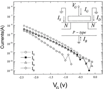
The n-channel MOSFETs with the gate width and length of 10 and 0.5m, respectively were manufactured in a stan-dard process technology. During the gate stack formation, a 10 Å thick SiO2 layer was thermally grown and underwent
rapid plasma nitridation共RPN兲 treatment, then on which a 10 Å thick nitride film was grown, followed by NO annealing at 950 °C. The devices were characterized by means of a semi-conductor parameter analyzer HP4156 with source, drain, and bulk tied to ground. The measured steady-state terminal currents versus negative gate voltage characteristics, as de-picted in Fig. 1 for a certain sample, were found to be nearly the same for all samples. From Fig. 1 we drew a certain EDT region of interest throughout the work: ⫺1.40 V⬍VG⬍
⫺0.88 V. In such a low voltage range, the EDT current IS
flowing from source to gate and the other EDT current ID
from drain to gate both dominantly constitute the gate cur-rent IG. Figure 1 further points out that the source and drain
currents are comparable each other in the sense of steady-state characterization. To strengthen RTS measurement pre-cision, the integration time in HP4156 for data sampling was changed from a default value of 1 ms down to equipment
limit of 8 s. The measured fluctuations in drain, gate, and source currents for the sample in Fig. 1 are displayed in Fig. 2, looking like those from a two-terminal tunnel gate stack with a percolation path.4 –7 The abrupt transitions between two distinct states occur in gate and source currents whereas being absent in the drain current, suggesting that 共i兲 signifi-cant defects exist in the gate-to-source overlap part rather than gate-to-drain overlap; and共ii兲 they should be localized such as to match above steady-state characterization. Figure 2 also reveals identical RTS parameters between source and gate currents: the same time durationonandoffin the high and low current state Ionand Ioff, respectively, and the same state current change⌬I (⫽Ion⫺Ioff). This consistency con-firms the existence of a two-terminal EDT path.
Figure 3 shows experimental Ion and Ioff of the source
current against gate voltage. We also found that 共i兲 the
sta-a兲Author to whom correspondence should be addressed; electronic mail:
FIG. 1. Measured steady-state terminal currents vs negative gate voltage. The inset shows the connection configuration.
APPLIED PHYSICS LETTERS VOLUME 81, NUMBER 18 28 OCTOBER 2002
3488
0003-6951/2002/81(18)/3488/3/$19.00 © 2002 American Institute of Physics
This article is copyrighted as indicated in the article. Reuse of AIP content is subject to the terms at: http://scitation.aip.org/termsconditions. Downloaded to IP: 140.113.38.11 On: Thu, 01 May 2014 06:07:07
tistical distributions ofon’s andoff’s indeed obey an
expo-nential behavior with the mean¯on and¯off, respectively;
and共ii兲¯onand¯offeach exponentially decrease with
increas-ing magnitude of gate voltage. Finally, repeated RTS mea-surements yielded the same RTS parameters, indicating that no stress induced defects are encountered, as expected due to low voltage operation.
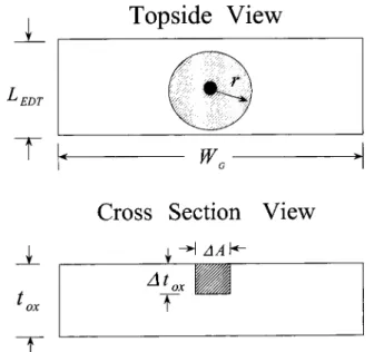
The above on–off switching phenomenon can be likely ascribed to the manufacturing process induced defects8,9 as schematically shown in Fig. 4 in terms of localized gate stack thinning, or equivalently the conductive filament9 de-fined by the thinning thickness ⌬tox and the occupied area
⌬A 共shaded region; shown only partly兲. Such a defective
spot can be thought to be a conductive filament connected in series with the remainder 共with the net thickness of tox
⫺⌬tox) of the gate stack. The conductive filament is also a
trap-rich region in nature as characterized by the trapping– detrapping probabilities7in terms of both the emission time
offand the capture timeonas mentioned above. According
to current trapping–detrapping theories,7once a single elec-tron is captured in the trap-rich region, the caused Coulomb repulsive force repels subsequently tunneling electrons, thus effectively turning off the influenced area around the trapped electron. This specific area can be represented by a capture cross-section area10denotedr2in Fig. 4. Consequently, the EDT current in the filled trap mode can be written as 共analo-gous to Simoen et al.’s work10兲
Ioff⬇Jn⫻共AEDT⫺r2兲, 共1兲
where Jn is the tunneling current density associated with the
gate stack thickness toxand AEDTis the EDT area. The region
r2can be recovered to the on state in the empty trap mode.
The corresponding high current state Ion can thereby be ex-pressed as
Ion⬇Jn⫻共AEDT⫺⌬A兲⫹⌬Jn⫻⌬A, 共2兲
where⌬Jnis the tunneling current density for a net thickness of tox⫺⌬tox, indicating that⌬JnⰇJnfor considerable⌬tox. The mentioned ‘‘localization’’ implies that ⌬A can be of comparable order with r2.9As a result, Eq.共2兲 minus Eq. 共1兲 produces quantitatively ⌬I⬇⌬Jn⫻⌬A for the
two-terminal characteristic of a defective spot. In Fig. 3 the frac-tional change⌬I/Ioffturns out to be between 12% and 18%.
Also plotted in Fig. 3 is a line from an empirical formula of direct tunneling for oxide thinning ⌬I⫽a兩VG兩b,6 showing
not only close agreements with experiment but also reason-able values of a and b compared with the citation.6
FIG. 2. Time records of drain, gate, and source currents at VG⫽⫺1.08 V for the sample in Fig. 1.
FIG. 3. Experimental high and low state currents vs magnitude of gate voltage for the sample in Fig. 1; also shown is a line for comparison.
FIG. 4. Topside and cross section views of a gate stack overlap part devoted to the edge direct tunneling operation, defined by the gate width WG, the effective tunneling size LEDT(⬃6 nm), and the thickness tox. On the topside a shaded circle with the trapped electron as the origin is drawn with a radius
r. On the cross section part a localized gate stack thinning or conductive
filament is drawn in terms of the thinning thickness⌬toxand the occupied area⌬A.
3489
Appl. Phys. Lett., Vol. 81, No. 18, 28 October 2002 M. Chen and M. Lu
This article is copyrighted as indicated in the article. Reuse of AIP content is subject to the terms at: http://scitation.aip.org/termsconditions. Downloaded to IP: 140.113.38.11 On: Thu, 01 May 2014 06:07:07
Furthermore we carried out a very extensive RTS mea-surement across the whole wafer. It turned out that about 36% of the samples exhibit two-level RTS only in EDT source currents; 12% only in EDT drain currents; and no noticeable RTS was observed for the rest or for both EDT source and drain currents. Therefore, systematic measure-ments of RTS in the terminal currents allow for determining the occurrence probability as well as locations of defects, and may be treated as a sensitive process monitor.
In conclusion, a new on–off switching behavior is mea-sured in the gate stack overlap EDT currents. With process defects as the plausible origin, experimental data can be ad-equately described by current trapping–detrapping theories. Significant efforts are also made: assessing the two-terminal current–voltage characteristic associated with a defective spot; finding the occurrence probability of the defects as well as their locations in a manufacturing process; etc.
This work was supported by the National Science Coun-cil under Contract No. 90-2218-E-009-043.
1
N. Yang, W. K. Henson, and J. J. Wortman, IEDM Tech. Dig. 453共1999兲.
2K. N. Yang, H. T. Huang, M. J. Chen, Y. M. Lin, M. C. Yu, S. M. Jang,
C. H. Yu, and M. S. Liang, Extended Abstracts of International Confer-ence on Solid State Devices and Materials共SSDM兲 共2000兲, p. 208.
3
K. N. Yang, H. T. Huang, M. J. Chen, Y. M. Lin, M. C. Yu, S. M. Jang, C. H. Yu, and M. S. Liang, IEDM Tech. Dig. 679共2000兲.
4K. R. Farmer, C. T. Rogers, and R. A. Buhrman, Phys. Rev. Lett. 58, 2255
共1987兲.
5B. Neri, P. Olivo, and B. Ricco`, Appl. Phys. Lett. 51, 2167共1987兲. 6
E. Miranda, J. Sun˜e´, R. Rodrı´guez, M. Nafrı´a, and X. Aymerich, Interna-tional Reliability Physics Symposium共IRPS兲 Proceedings 共1998兲, p. 42.
7I. Polishchuk, T. J. King, and C. Hu, Device Research Conference共DRC兲,
Conference Digest共2001兲, p. 20.
8K. F. Schuegraf and C. Hu, IEEE Trans. Electron Devices 41, 761共1994兲. 9
H. T. Huang and M. J. Chen, Extended Abstracts of International Confer-ence on Solid State Devices and Materials共SSDM兲 共2000兲, p. 246.
10E. Simoen, B. Dierickx, C. L. Claeys, and G. J. Declerck, IEEE Trans.
Electron Devices 39, 422共1992兲.
3490 Appl. Phys. Lett., Vol. 81, No. 18, 28 October 2002 M. Chen and M. Lu
This article is copyrighted as indicated in the article. Reuse of AIP content is subject to the terms at: http://scitation.aip.org/termsconditions. Downloaded to IP: 140.113.38.11 On: Thu, 01 May 2014 06:07:07