The structural and optical properties of ZnO nanowire arrays
prepared by hydrothermal synthesis method
Shr-Nan BaiÆ Tseung-Yuen Tseng
Received: 24 May 2008 / Accepted: 1 July 2008 / Published online: 24 July 2008 Ó Springer Science+Business Media, LLC 2008
Abstract ZnO nanowire arrays have been grown on the ZnO film-coated silicon (100) substrates by hydrothermal method, and the deposited nanowires are found to have a uniform size distribution with sharp hexagonal-shaped tips. The structural and optical properties of the nanowires were investigated using atomic force microscopy (AFM), X-ray diffraction (XRD), scanning electron microscopy (SEM), transmission electron microscopy (TEM), and cathodolu-minescence (CL) techniques. The XRD and SEM results demonstrate that the well-aligned ZnO nanowires are sin-gle crystalline structure formed along the c-axis orientation. TEM analysis further confirms that the ZnO nanowires are highly preferred grown along the (002) crystal plane. The spacing between adjacent (002) lattice planes is estimated as 0.52 nm. The optical properties of the nanowires were measured using CL after annealing in oxygen and nitrogen atmospheres at 550°C for various times. The CL spectra in the visible spectrum exhibit two weak deep-level emission bands that may be attributed to the intrinsic or extrinsic defects. It can be observed that the ZnO nanowires show different optical behaviors after various annealing times. The dependence of the optical properties on the annealing conditions is also discussed.
1 Introduction
Zinc oxide (ZnO) nanowires have recently attracted con-siderable attention because of their potential technological applications in the areas of field emission, laser emission, and nanoscale heterojunction [1–5]. Owing to wide direct band gap of 3.37 eV and large exciton binding energy of 60 meV at room temperature, ZnO becomes a more superior candidate for optoelectronic utilizations than the other wide band gap materials such as GaN and SiC. One-dimensional (1D) ZnO nanostructures with different shapes and morphologies are easily prepared by using various physical, chemical, or electrochemical methods [6–11] due to easy growth along the c-axis of the wurtzite hexagonal structure. Among these fabrication methods, ZnO nano-wires are most commonly grown by vapor phase methods like vapor–liquid–solid (VLS), chemical vapor transport, and thermal evaporation [7–9]. These approaches can produce high quality and vertically aligned nanowires array with a length of several microns. However, these fabrica-tion procedures require higher temperatures ranging from 450 to 900°C. The complex processes and high cost vac-uum equipments are often involved in these technologies as well. Moreover, the other limitations in terms of crystal uniformity, matched substrate, and sample yield are also frequently met. Compared with those techniques, chemical solution method is attractive to synthesize ZnO nano-structures because of the low cost equipments, lower growth temperatures, promising for scaling up, and con-trolled easily technology of growing high-density nanowires array [12]. In this paper, the synthesis of ZnO nanowires from zinc salts in aqueous solution is studied through adjusting the concentration of zinc nitrate; then, the resultant variation of morphology, structure, and optical property is discussed.
S.-N. Bai (&)
Department of Electronic Engineering, Institute of Electronic, Chienkuo Technology University, Changhua City 500, Taiwan, ROC
e-mail: [email protected] T.-Y. Tseng
Department of Electronics Engineering, Institute of Electronics, National Chiao-Tung University, Hsinchu City 300,
Taiwan, ROC
e-mail: [email protected] DOI 10.1007/s10854-008-9772-4
2 Experimental
Vertically aligned ZnO nanowires were synthesized on the p-type silicon (Si) substrates through a ZnO-seed-assisted hydrothermal method without the presence of metal cata-lysts. Prior to the growth of ZnO nanowires, the Si substrates (100) were cleaned by a standard Radio Corporation of America (RCA) cleaning method and rinsed in acetone for 30 min to remove pollutants. Then, the ZnO seed-layer film about 40 nm in thickness were deposited on Si substrates by the conventional radio-frequency (RF) magnetron sputtering with argon as working gas, and subsequently in-situ annealing at 550°C for 3 h. X-ray diffraction measurement demonstrated that the sputtered ZnO seed-layer film was oriented along the c-axis preferred direction (not shown here). The 0.08–0.16 M aqueous solutions of zinc nitrate hexahydrate (99.9% purity) and hexamethylenetetramine (HMT; 99.9% purity) were prepared. Then, the Si substrate with ZnO seed-layer film was placed in the aqueous solution and maintained at 95°C with stable stirring in thermostati-cally controlled bath for 3 h. The as-grown ZnO nanowires were rinsed in deionized water and then dried in air for fur-ther characterization and analysis.
The surface roughness of the ZnO seed-layer film was observed by the atomic force microscopy (AFM) using a silicon nitride tip in contact mode. The crystalline structure and orientation of the nanowires was characterized by the X-ray diffractometry using CuKa (k = 1.5418 A˚ ) radia-tion. The morphology and the microstructure of the ZnO nanowires over the substrates were investigated by using field-emission scanning electron microscopy (FE-SEM) and transmission electron microscopy (TEM), respectively. The optical properties were analyzed using the cathodolu-minescence (CL) with an electron beam as an excitation source (15 kV) at room temperature.
3 Results and discussion
Figure1shows the high magnification AFM image of the sputtered ZnO seed-layer film. The figure scans over an area of 500 nm 9 500 nm. The film exhibits the rough surface with recognizable ZnO nano-aggregations and roughness approximately 3 nm. The seed-layer film sig-nificantly varies the surface characteristics of the Si substrates and then alters the synthesis of the ZnO nano-wires since that the zinc oxide or suboxide cluster film was used as the nucleation center to adjust the growth direction of ZnO nanowires [13,14].
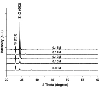
Figure2shows the XRD patterns of the ZnO nanowires grown on the ZnO film/Si substrates. The sharp diffraction peaks reveal that the ZnO nanowires show high crystallinity
of wurtzite hexagonal structure with lattice constants of a = 0.32 nm and c = 0.52 nm, which are in good agree-ment with the reported values of ZnO bulk crystal (JCPDS card No. 36-1451). Additionally, the diffraction patterns of the nanowires exhibit pronounced stronger peak intensity of (002) crystal plane compared with that of bulk crystal showing the maximum intensity of (101) crystal plane. Therefore, the XRD data are verified that the ZnO nanowires have been synthesized with preferred orientation along the c-axis perpendicular to the substrate surface. From the experimental results above, it is shown that the ZnO nano-wires can be effectively grown at a low temperature (95°C) by ZnO-seed-assisted hydrothermal method. Such a low temperature synthesized method can broaden many various applications of optoelectronic devices that prepared under low-temperature fabrication procedures.
Fig. 1 AFM image of ZnO seed-layer thin film
30 35 40 45 50 55 60 Si (201) ZnO (002) Intensity (a.u.) 2 Theta (degree) 0.08M 0.10M 0.12M 0.14M 0.16M
Fig. 2 XRD patterns of the ZnO nanowires synthesized in aqueous solution with various molar concentrations of zinc nitrate for 3 h
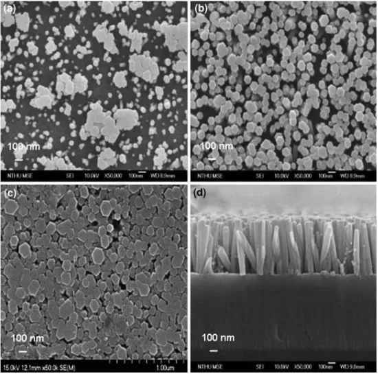
Figure3a–d illustrates the top-view and cross-sectional FE-SEM images of ZnO nanowires fabricated at various concentrations of aqueous solution. The nanowires with uniformity in their diameters and lengths are produced successfully on ZnO film-coated Si substrates by hydro-thermal technique. It can be observed the concentration of aqueous solutions plays a crucial role in the synthesis of the nanowires. The SEM images reveal that morphologies of the ZnO nanowires synthesized by various solution con-centrations are apparently different. With dependence on the concentration of aqueous solution, the diameters of the nanowires are demonstrated to increase with an increase of solution concentration in the range of 0.08–0.16 M. The average diameters of the ZnO nanowires for solution concentration of 0.08, 0.12, and 0.16 M are 36, 95, and 127 nm, respectively. Further structural characterizations of the ZnO nanowires are studied by TEM and HRTEM.
Figure4a shows the TEM image of a well-developed ZnO nanowire with diameter approximately 65 nm in accordance with the SEM measurement. It displays that the
synthesized nanowire is really straight and has a smooth surface. The diameters of the nanowires are found to slightly decrease from the root to the tip along their lengths. The lattice-resolved HRTEM image pattern mea-sured from one individual nanowire is shown in Fig. 4b. The crystal lattice fringes are clearly observed without any defects produced during the growth processes and average distance between the adjacent lattice planes is 0.52 nm. This measured plane spacing is characteristic of the (002) planes, showing the ZnO nanowire with perfect lattice structure and is verified again that the nanowires grow along the c-axis direction.
Figure5a–b demonstrates the room temperature CL spectra of ZnO nanowires thermally annealed at oxygen and nitrogen atmospheres with different reaction times. It is found that the annealing atmosphere and reaction time have remarkable effects on the optical properties of ZnO nano-wires. In Fig.5, the as-grown ZnO nanowires show a broad green-yellow emission band with an emission peak approx-imately 575 nm and a much narrow orange-red emission Fig. 3 FE-SEM images of the ZnO nanowires synthesized in aqueous solution with various molar concentration of zinc nitrate for reaction time 3 h (a) 0.08 M: top-view; (b) 0.12 M: top-view; (c) 0.16 M: top-view; (d) 0.12 M: cross-section-view
peak around 625 nm. The visible emission peaks (575 and 625 nm) in this study are reasonably assumed resulted from some deep-level defects. The CL spectrum of ZnO can be generally separated into two emission regions. One is located in the UV region corresponding to the near band-edge emissions attributed to the electron-hole pair recombination. The other is located in the visible region coming from some intrinsic or extrinsic defects. Based on these studies [15–19], the origin of the green-yellow emission around 575 nm is believed due to the absorbed water or surface hydroxyl (OH) groups while the orange-red emission at around 625 nm is resulted from the oxygen interstitials.
In addition, no matter the ZnO nanowires annealed in oxygen or nitrogen atmosphere, the green-yellow emission centering at around 575 nm disappears and the orange-red emission at about 625 nm is decreased as the annealing time increased, and the decrease of peak intensity (625 nm) in oxygen is more quickly than that in nitrogen atmosphere. It indicates that the oxygen interstitial defect states in the nanowires annealed in nitrogen atmosphere may have lower localization energy than that annealed in oxygen atmo-sphere. Moreover, the variation of the emission peak in the visible spectrum with annealing atmosphere suggests that the optical properties of the ZnO nanowires are tunable which will be quite useful for the optoelectronic applications.
4 Conclusions
The high quality ZnO nanowires have been successfully synthesized on ZnO film-coated silicon substrates by a simple, low cost, and reproducible hydrothermal technique. XRD and SEM measurements demonstrate that the ZnO nanowires are single crystal phase with wurtzite structure. Fig. 4 (a) TEM image of the ZnO nanowire synthesized at solution concentration 0.12 M of zinc nitrate; (b) HRTEM image taken from an individual ZnO nanowire
Wavelength (nm) Wavelength (nm) (a) Intensity (a.u.) – – 0h – – 1h – – 3h – – 5h 625 nm 575 nm 450 500 550 600 650 700 450 500 550 600 650 700 Intensity (a.u.) (b) – – 0h – – 1h – – 3h – – 5h 575 nm 625 nm
Fig. 5 Visible CL spectra of the ZnO nanowires thermal annealed at 550°C for different reaction times in (a) oxygen, (b) nitrogen atmospheres
TEM and HRTEM are used to observe the fine structure of the nanowires. The results exhibit that the ZnO nanowire are highly preferential growth in the c-axis direction with lattice spacing of 0.52 nm. CL spectra of the as-grown and annealed ZnO nanowires are studied as well. The oxygen or nitrogen thermal annealing is confirmed as an effective method to change the visible luminescence emissions. Absorbed water or surface hydroxyl (OH) groups is believed to result in the green-yellow emission around 575 nm, and oxygen interstitial the main factor on the orange-red emission about 625 nm.
Acknowledgements The authors gratefully appreciate the financial support from the National Science Council of Republic of China under Project Numbers NSC 95-2221-E009-120 & NSC 96-2221-E270-003. Mr. H. H. Tsai is thanked for his help in experimental works.
References
1. C.Y. Lee, S.Y. Li, P. Lin, T.Y. Tseng, IEEE Trans. NanoTechnol. 5, 216–219 (2006). doi:10.1109/TNANO.2006.874049
2. S.H. Jo, J.Y. Lao, Z.F. Ren, R.A. Farrer, T. Baldacchini, J.T. Fourkas, Appl. Phys. Lett. 83, 4821–4823 (2003). doi:10.1063/ 1.1631735
3. C. Liu, J.A. Zapien, Y. Yao, X. Meng, C.S. Lee, S. Fan et al., Adv. Mater. 15, 838–841 (2003). doi:10.1002/adma.200304430 4. M.H. Huang, S. Mao, H. Feick, H. Yan, Y. Wu, H. Kind et al.,
Science 292, 1897–1899 (2001). doi:10.1126/science.1060367
5. W.I. Park, G.C. Yi, J.W. Kim, S.M. Park, Appl. Phys. Lett. 82, 4358–4360 (2003). doi:10.1063/1.1584089
6. Y. Zhang, N. Wang, S. Gao, R. He, S. Miao, J. Liu et al., Chem. Mater. 14, 3564–3568 (2002). doi:10.1021/cm0201697 7. D. Banerjee, J.Y. Lao, D.Z. Wang, J.Y. Huang, Z.F. Ren, D.
Steeves et al., Appl. Phys. Lett. 83, 2061–2063 (2003). doi: 10.1063/1.1609036
8. S.Y. Li, C.Y. Lee, T.Y. Tseng, J. Cryst. Growth 247, 357–362 (2003). doi:10.1016/S0022-0248(02)01918-8
9. J.J. Wu, S.C. Liu, Adv. Mater. 14, 215–218 (2002). doi:10.1002/ 1521-4095(20020205)14:3\215::AID-ADMA215[3.0.CO;2-J 10. P.C. Chang, Z. Fan, D. Wang, W.Y. Tseng, W.A. Chiou, J. Hong
et al., Chem. Mater. 16, 5133–5137 (2004). doi:10.1021/cm04 9182c
11. M.J. Zheng, L.D. Zhang, G.H. Li, W.Z. Shen, Chem. Phys. Lett. 363, 123–128 (2002). doi:10.1016/S0009-2614(02)01106-5 12. L.E. Greene, M. Law, J. Goldberger, F. Kim, J.C. Johnson, Y.
Zhang et al., Angew. Chem. Int. Ed. 42, 3031–3034 (2003). doi: 10.1002/anie.200351461
13. D.H. Liu, L. Liao, J.C. Li, H.X. Guo, Q. Fu, Mater. Sci. Eng. B 121, 77–80 (2005). doi:10.1016/j.mseb.2005.03.005
14. L.E. Greene, B.D. Yuhas, M. Law, D. Zitoun, P. Yang, Inorg. Chem. 45, 7535–7543 (2006). doi:10.1021/ic0601900
15. Y.C. Kong, D.P. Yu, B. Zhang, W. Fang, S.Q. Feng, Appl. Phys. Lett. 78, 407–409 (2001). doi:10.1063/1.1342050
16. Y.P. Wang, W.I. Lee, T.Y. Tseng, Appl. Phys. Lett. 69, 1807– 1809 (1996). doi:10.1063/1.117493
17. R. Xie, D. Li, D. Yang, T. Sekiguchi, M. Jiang, Nanotechnology 17, 2789–2793 (2006). doi:10.1088/0957-4484/17/11/011 18. X.L. Wu, G.G. Siu, C.L. Fu, H.C. Ong, Appl. Phys. Lett. 78,
2285–2287 (2001). doi:10.1063/1.1361288
19. S.N. Bai, H.H. Tsai, T.Y. Tseng, Thin Solid Films 516, 155–158 (2007). doi:10.1016/j.tsf.2007.06.096