Strain relaxation in InAs self-assembled quantum dots induced by a high N
incorporation
J. F. Chen, C. H. Yang, Y. H. Wu, L. Chang, and J. Y. Chi
Citation: Journal of Applied Physics 104, 103717 (2008); doi: 10.1063/1.3028235 View online: http://dx.doi.org/10.1063/1.3028235
View Table of Contents: http://scitation.aip.org/content/aip/journal/jap/104/10?ver=pdfcov Published by the AIP Publishing
Articles you may be interested in
Strain study of self-assembled InAs quantum dots by ion channeling technique J. Appl. Phys. 100, 103502 (2006); 10.1063/1.2382421
Strain relaxation and induced defects in InAsSb self-assembled quantum dots Appl. Phys. Lett. 88, 233113 (2006); 10.1063/1.2212064
Strain status of self-assembled InAs quantum dots Appl. Phys. Lett. 77, 1295 (2000); 10.1063/1.1290152
Strain relaxation and segregation effects during self-assembled InAs quantum dots formation on GaAs(001) Appl. Phys. Lett. 77, 409 (2000); 10.1063/1.126992
Strain relaxation-induced modifications of the optical properties of self-assembled InAs quantum dot superlattices J. Vac. Sci. Technol. B 18, 1493 (2000); 10.1116/1.591411
Strain relaxation in InAs self-assembled quantum dots induced by a high N
incorporation
J. F. Chen,1,a兲C. H. Yang,1Y. H. Wu,2L. Chang,2and J. Y. Chi3
1
Department of Electrophysics, National Chiao Tung University, Hsinchu 300, Taiwan, Republic of China
2
Department of Materials Science and Engineering, National Chiao Tung University, Hsinchu 30010, Taiwan, Republic of China
3
Industrial Technology Research Institute (OES/ITRI), Hsinchu 310, Taiwan, Republic of China
共Received 1 July 2008; accepted 8 October 2008; published online 24 November 2008兲
The effect of a high N incorporation in self-assembled InAs quantum dots共QDs兲 is investigated by analyzing the electronic and structural properties around QD region. Capacitance-voltage profiling and admittance spectroscopy shows that N incorporation into the InAs QD layer leads to drastic carrier depletion in the QD layer and neighboring GaAs layers due to the formation of a deep defect state at 0.34–0.41 eV. The signature of this defect state is similar to those defects observed in strain relaxed QDs or InGaAs/GaAs quantum wells when the InAs deposition thickness exceeds a critical thickness. Accordingly, the N incorporation might result in strain relaxation either by increasing localized strain or by inducing composition inhomogeneities, which provide nucleation sources for strain relaxation. The argument of strain relaxation is supported by transmission electron microscopy that reveals lattice misfits at the QD layer and neighboring GaAs layers. © 2008
American Institute of Physics.关DOI:10.1063/1.3028235兴
I. INTRODUCTION
Self-assembled quantum dots 共QDs兲 共Refs. 1–19兲 have recently attracted a great deal of attention due to their scien-tific studies and promising technological applications. There is increasing interest in extending the emission wavelength for communication applications. Capping InAs QDs by a strain reducing InGaAs layer can achieve the wavelength extension16 by enlarging the dot size. Incorporating N atoms into the InGaAs cap layer can further redshift the emission by penetrating the wave function into the cap layer due to the reduction in the potential barrier of the cap layer.17,18 How-ever, this wavelength extension is rather limited. N atoms can also be incorporated directly into an InGaAs QD layer to form GaInNAs QDs for achieving a long emission wavelength.19 Unfortunately, photoluminescence 共PL兲 spec-tra are severely degraded at a high N content.19This degra-dation is usually attributed to a formation of deep levels such as bulk20or interfacial21traps observed in共In兲GaAsN alloys grown on GaAs. However, the origin of these defects has not yet been established. In a previous work,22an abnormal blue-shift of the emission wavelength was observed when a high N content was incorporated into an InAs QD layer. The PL spectra became very broad and asymmetric with a very long low-energy tail extending to 1.5 m.22In this study, we con-tinue this work to characterize the detailed electronic and structural properties of the QDs in order to establish the un-derlying reasons for the PL degradation and the abnormal N-incorporation induced blueshift. We showed that the N incorporation led to drastic carrier depletion near the QD region due to an induction of a deep defect state at 0.34–0.41 eV. The signature of this defect is similar to those states observed in strain relaxed InAs QDs and InGaAs/GaAs
quantum wells共QWs兲 when the InAs or the InGaAs deposi-tion thickness exceeds a critical thickness, suggesting that the N incorporation might lead to localized strain relaxation of the QDs. This conclusion is supported by the cross-sectional transmission electron microscopy 共TEM兲 that shows lattice misfits near the QD region. Accordingly, the abnormal PL blueshift is attributed to strain relaxation, con-sistent with the previous observation of a blueshift23 when strain relaxation in InAs QDs occurs by increasing the InAs deposition thickness beyond a critical thickness.
II. EXPERIMENTS
Samples were grown on an n+-GaAs共100兲 substrate by
molecular beam epitaxy in a Riber Epineat machine. An InAs QD structure consisting of a 2.4 ML共monolayer兲 InAs layer and a 60 Å In0.15Ga0.85As cap layer grown at a rate of 1.86 Å/s at 480 °C, was sandwiched between two 0.3 m thick Si-doped GaAs 共⬃7⫻1010 cm−3兲 barrier layers.
In-dium and gallium were supplied from Knudsen cells, and As in the form of As2 was supplied from a cracker source. N
atoms were incorporated into the InAs layer using an EPI-Unibulb radio-frequency plasma source to supply active ni-trogen species from ultrapure N2gas. Assuming the added N
is completely incorporated into the InAs sublattice, we esti-mated the N content to be 17% from the growth rates of the InAs共0.26 Å/s兲 and GaAs 共2.78 Å/s兲 layers assuming the N incorporation efficiency is similar to that in GaAsN layer.24 Such a high N composition is due to the very low growth rate of the InAs QD layer for gaining a high density of the QDs. If the same N source is incorporated into a GaAs layer at a growth rate of 2.78 Å/s, the resulted N composi-tion would be about 2%. Schottky diodes were realized by evaporating Al with a dot diameter of 1500 m after a slight chemical etch on the sample surface.
a兲Electronic mail: [email protected].
0021-8979/2008/104共10兲/103717/5/$23.00 104, 103717-1 © 2008 American Institute of Physics [This article is copyrighted as indicated in the article. Reuse of AIP content is subject to the terms at: http://scitation.aip.org/termsconditions. Downloaded to ] IP:
III. MEASUREMENT AND RESULTS A. Capacitance-voltage„C-V… profiling
The effect of N incorporation on the electronic proper-ties of the QDs is illustrated in Fig. 1共a兲, which shows the free-electron depth profiles converted from room-temperature C-V curves at a high modulating frequency of 105 Hz for 2.4 ML InAs QDs with and without N
incorpo-ration. The InAs QDs 共without N incorporation兲 shows strong electron accumulation at the QDs and nearly symmet-ric carrier depletion with a valley concentration of 5 ⫻1016 cm−3 on both sides of the QDs. The peak position
共0.27 m兲 is slightly less than the expected QD depth of 0.3 m, which is due to a slight chemical etching on the sample surface before Schottky metal evaporation. When temperature is lowered, a right shoulder共at a larger reverse bias兲 can be resolved from the carrier peak. The main peak and the shoulder are attributed to the depopulation of the QD excited states and the ground state, respectively. The
emis-sion time from the shoulder 共QD ground state兲 can be re-solved to yield an activation energy Ea of ⬃58 meV,25 which is close to the energy difference between the ground and first-excited PL transitions. Accordingly, the shoulder is attributed to electron emission from the QD ground to the first-excited state and a subsequent tunneling to the bottom GaAs. Detailed properties of this two-stage emission process can be found elsewhere.15,25
Upon N incorporation, the carrier distribution is changed to drastic carrier depletion共with a deepest valley concentra-tion of 8⫻1015 cm−3兲 around the QD. The carrier depletion can be seen to extend far into the GaAs barrier layers. This carrier distribution suggests the presence of a deep defect state, which traps the electrons in the QD states and neigh-boring GaAs layers. Due to a long emission time of the de-fect state, the electron emission from the dede-fect state is inca-pable of following the modulated frequency 共F=105 Hz兲. Increasing temperature or lowering modulating frequency can reduce the emission time and allow for the modulation of the electrons trapped on the defect state. As shown in Figs. 1共b兲and1共c兲, for T⬎300 K and at F=3 kHz, an additional capacitance plateau emerges from −1.5 to −2.5 V, which converts to a peak with a large full width at half maximum 共FWHM兲 of ⬃20 nm 共at 350 K兲. The long tail on both side of the peak in Fig.1共c兲suggests the spatial extension of the defect state into neighboring GaAs layers. Since the peak position共0.31 m兲 in Fig.1共c兲represents the position of the edge of the depletion region when Fermi level intersects the defect state, the FWHM of 20 nm corresponds to an energy downward shift of about 100 meV for the Fermi level at a depth of 0.3 m, based on a simple Schottky depletion model. Thus, the defect state is considered to have a spectral broadness of about 100 meV.
B. Admittance spectroscopy
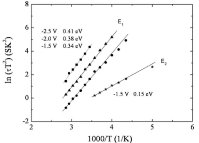
The energy position of the defect state is obtained from the activation energy of the electron emission from the defect state by performing admittance spectroscopy on the capaci-tance plateau 共from −1.5 to −2.5 V兲 in Fig. 1共b兲. Figures 2共a兲–2共c兲 show the conductance/frequency-frequency 共G/ F-F兲 spectra for −1.5, −2, and −2.5 V, respectively, mea-sured at several temperatures as shown共with a step of 10 K兲. The conductance will reach a peak when frequency is com-parable to the emission rate. A strong peak E1is seen at the
three voltages and a very weak peak E2 is seen only at
−1.5 V. From their Arrhenius plots, emission energies 共cap-ture cross sections兲 of E1 are determined to be 0.34 eV
共4.16⫻10−16 cm2兲, 0.38 eV 共5.74⫻10−16 cm2兲, and 0.41
eV 共3.10⫻10−16 cm2兲 for −1.5, −2, and −2.5 V,
respec-tively, as shown in Fig. 3. Treating the different activation energies as a spectral broadness, this defect state E1 lies at
⬃0.38 eV with a linewidth broadness of about 70 meV, which is comparable to the value estimated from the FWHM of the peak in Fig. 1共c兲. Since the defect extends into the GaAs barrier layers, it is reasonable to assume that the ob-served emission energy is related to the GaAs conduction band. Thus, the defect state shall lie at⬃0.38 eV below the GaAs conduction band. Kapteyn et al.15 estimated the
con-FIG. 1.共a兲 Depth profiles of the N-incorporated InAs QD and a reference InAs QD without N incorporation measured at 300 K and 105 Hz. N incor-poration induces a defect state that results in drastic carrier depletion in the QD and neighboring GaAs layers.共b兲 Temperature-dependent C-V and 共c兲 the corresponding depth profiles of the N-incorporated InAs QD, illustrating a C plateau共from −1.5 to −2.5 V兲 and a corresponding peak related to electron emission from the defect state.
103717-2 Chen et al. J. Appl. Phys. 104, 103717共2008兲
finement energy of 0.19 eV for the electron ground state 共EGS兲 of InAs QDs emitting a wavelength close to our N-incorporated InAs QDs共⬃1.02 eV at 300 K兲. Taking this
energy for the EGS, the defect state would be ⬃0.19 eV below the EGS, allowing for the carrier depletion of the QDs.
As to the origin of the weak emission E2whose emission
energy 共capture cross section兲 is determined to be 0.15 eV 共1.46⫻10−18 cm2兲 as shown by its Arrhenius plots in Fig.3,
it is only observed at −1.5 V and thus it is spatially confined in a very narrow QD layer. This emission is very weak and thus the experimental uncertainty for the activation energy is rather large. It could be another defect state induced by N incorporation or an electron emission from the QD state. Postgrowth thermal annealing is found to enhance the E2
emission and diminish the E1 emission, suggesting that
an-nealing can remove the defect state at⬃0.38 eV, which can in turn lead to a recovery of electrons in the QDs. Accord-ingly, the E2 emission is tentatively assigned to an emission
from the QD state. Our experimental data show no apparent redshift by incorporating N into the InAs QD deposition layer. This observation leads us to suspect that either the InAs band gap is not reduced by N substitution of As sub-lattice or the incorporated N atoms do not occupy the As sublattice. If the incorporated N atoms do not occupy the As sublattice, they are likely in defect sites. We found that a postgrowth thermal annealing can redshift the PL emission from the InGaAs cap layer, suggesting a diffusion of the incorporated N atoms into the InGaAs cap layer to form an InGaAsN cap layer during annealing. Hence, the incorpo-rated N atoms actually enter into the InAs QDs during the growth. Thermal annealing can diffuse the N atoms to the InGaAs cap layer, leading to the recovery of free electrons in the QDs and the emission from the QD states, E2. Further
investigation is currently underway to make further argu-ment.
To establish the origin of the defect state E1共0.38 eV兲,
Fig. 4 compares its Arrhenius plots 共the solid circles兲 with the previously observed plots of those defects reported in relaxed 3.4 ML InAs QDs,26 3.3 ML InAs QDs with an In-GaAs capping layer,25 relaxed 2.8 ML InAsSb QDs,27 and relaxed InGaAs/GaAs QW.28 These plots are comparable,
FIG. 2. G/F-F spectra of the N-incorporated InAs QD measured at 共a兲 −1.5 V,共b兲 −2 V, and 共c兲 −2.5 V, respectively. A dominant E1peak with 0.34, 0.38, and 0.41 eV can be seen for −1.5, −2, and −2.5 V, respectively. This peak is attributed to an emission from the N-induced defect state. Aside from this peak, the G/F spectra at −1.5 V show another weak peak E2with 0.15 eV, which is tentatively attributed to an emission from the QD state.
FIG. 3. Arrhenius plots of the E1and E2states observed in the G/F spectra in the N-incorporated InAs QDs.
FIG. 4. Arrhenius plots of the E1defect state induced by N incorporation and previously observed plots of the defect states in relaxed 3.4 ML InAs QDs共Ref.26兲, 3.3 ML InAs QDs with an InGaAs capping layer 共Ref.25兲,
relaxed 2.8 ML InAsSb QDs共Ref.27兲, and relaxed InGaAs/GaAs QW 共Ref. 28兲. The comparability suggests that the E1defect state is associated with strain relaxation in the QDs.
suggesting that the defect E1is likely related to strain
relax-ation in the QDs. This comparability also suggests that the nature of the defect is only related to strain relaxation, irrel-evant of QD or QW or In or Sb composition. Hence, the N incorporation might lead to strain relaxation either by in-creasing the strain between the QD and the GaAs barrier layers or providing nucleation sites for strain relaxation. This 0.38 eV defect state can also be detected by deep-level tran-sient spectroscopy.22 As those defects in the above refer-ences, the peak amplitude of this defect state displays a satu-ration of its amplitude with increasing filling pulse dusatu-ration time, suggesting a regular point-defectlike property in con-trast to threading dislocations that show an unsaturated loga-rithmic dependence on filling pulse duration time.29This re-sult suggests a high structural regularity for the defects induced by strain relaxation. These defects are well confined near the relaxed QD or QW region, in contrast to threading dislocations that penetrate deep into the GaAs barrier layer.26,27
C. TEM characterization
To clarify whether the QDs are strain relaxed, Fig. 5 shows the cross-sectional TEM picture of the N-incorporated QD sample. A line of the QDs can be seen共the wetting layer is indicated by a line for guiding the eyes兲. In contrast to the QDs without N incorporation, the color contrast of QDs is unclear, and thus precise determination of dot size is diffi-cult. A rough estimation is⬃10 nm in height and ⬃20 nm in base width. To illustrate detailed structures, we show the Fourier transformed image in the neighboring top GaAs layer, in the QD, and in the neighboring GaAs bottom layer 共indicated by 共a兲, 共b兲, and 共c兲, respectively兲. A significant number of lattice misfits共encircled兲 can be seen in all three areas. Their Fourier images are similar as those previously observed in relaxed InAs QDs.30 Note that no such misfits are observed in 2.4 ML thick InAs QDs without N
incorpo-ration. Although N is only incorporated during the deposition of the InAs QD layer, the misfits are observed in the neigh-boring GaAs barrier layers and in the intervening GaAs re-gion between the QDs. These misfits do not propagate deep into the GaAs barrier layers; they are confined around the QD of about 60 nm in total thickness. This spatial distribu-tion is consistent with that of the 0.38 eV defect state, which displays long tails on both sides of the emission peak共at 350 K兲 as shown in Fig. 1共c兲. These misfits act as the electron-trapping defect state, and since most of the misfits are lo-cated in the GaAs material 共rather than in the QDs兲, the observed electron emission process should be relative to the GaAs conduction band, as assumed for the 0.38 eV defect state above. These misfits are well confined near the QD layer, rather than penetrating deep into the top or bottom GaAs layers. They have much higher structural and elec-tronic regularity than threading dislocations, consistent with the defect states associated with lattice misfits.25,27These re-sults support that N incorporation into the InAs QD layer results in strain relaxation in the QDs. This could occur ei-ther by increasing the strain between QD and GaAs layers or induced defects, which provide nucleation sites for strain re-laxation. However, as in GaAs, N substitution of As in InAs is expected to decrease lattice constant, which would de-crease the lattice mismatch between the QD layer and the GaAs layers and reduce strain. Hence, we tend to exclude the strain increase as the cause for relaxation. On the other hand, due to a large difference between the radii of As and N atoms, a high N incorporation into As-related alloys often leads to significant composition fluctuation or even phase separation,19 although the lattice mismatch with the GaAs layers is decreased. Thus, the composition inhomogeneity caused by N incorporation is attributed to the cause for strain relaxation of the QDs. The composition inhomogeneity may lead to the very long low-energy tail up to 1.5 m共Ref.22兲 observed in the PL spectra. The carrier depletion caused by the misfit related defect state can lead to a large conduction-band protrusion in the vicinity of the QD, preventing the photogenerated carriers from entering the QD layer and de-grading the PL emission.
Strain relaxation in the QDs can cause blueshift of the PL emission. In the previous work,23when the InAs deposi-tion thickness is below the critical thickness 共⬃3 ML兲 for strain relaxation, increasing InAs deposition thickness can redshift the emission due to an increase in dot size. However, when the InAs deposition thickness is further increased from 2.7 to 3.06 ML, the PL emission undergoes an abnormal blueshift of 68 meV共from 1310 to 1223 nm at 300 K兲. This blueshift is accompanied with the generation of lattice mis-fits and the 0.38 eV defect state. Hence, the blueshift is ex-plained by the relief of built-in strain. Before relaxation, due to the underlying GaAs layer, the InAs QD is compressed perpendicular to the growth direction, giving rise to tensile strain in the QDs along the growth direction. Since the dot height is much smaller than the lateral dimension, the size-confinement effect and the related PL emission shift are dominated by the lattice constant along the growth direction. The tensile strain along the growth direction can extend the dot height, which extends the emission wavelength. Strain
FIG. 5. 共Color online兲 Cross-sectional TEM picture of the N-incorporated InAs QD共the top figure on the left兲. The wetting layer is indicated by a line for guiding the eyes. Figures indicated by共a兲, 共b兲, and 共c兲 are the Fourier transformed images for the area in the neighboring top GaAs layer, in the QD, and in the neighboring GaAs bottom layer, respectively. Significant lattice misfits can be clearly seen, as indicated by the circles.
103717-4 Chen et al. J. Appl. Phys. 104, 103717共2008兲
relaxation relives this strain and causes a blueshift. This can explain the observed blueshift from 1215 to 1060 nm共at 50 K兲 when N is incorporated into the InAs layer.22
IV. CONCLUSIONS
A high N incorporation into the InAs QD layer is shown to change the carrier distribution from accumulation to dras-tic depletion near the QD. When temperature is increased and frequency is lowered, a broad peak emerges from the depletion region. This peak is interpreted as an electron emission from a deep defect state. Admittance spectroscopy reveals an emission energy of⬃0.38 eV for this defect state. Judging from its Arrhenius plots, this defect state is likely the state previously observed in strain relaxed QDs or relaxed InGaAs/GaAs QW, suggesting that N incorporation might result in strain relaxation in the QDs. This argument is con-firmed by the TEM data that clearly show lattice misfits in the QD layer and the neighboring GaAs layers. From their similar spatial distribution, the 0.38 eV defect state is attrib-uted to the lattice misfits. Hence, N incorporation results in strain relaxation in the QDs by the accommodation of the lattice misfits, which act as electron-trapping centers to de-plete the electrons in the QDs.
ACKNOWLEDGMENTS
The authors would like to thank Dr. R. S. Hsiao for sample preparation, the National Science Council of the Re-public of China, Taiwan for financially supporting this re-search under Contract No. NSC-97-2112-M-009-014-MY3, and the MOE, ATU program.
1F. Heinrichsdorff, M.-H. Mao, N. Kirstaedter, A. Krost, and D. Bimberg, Appl. Phys. Lett.71, 22共1997兲.
2H. Saito, K. Nishi, and S. Sugou,Appl. Phys. Lett.73, 2742共1998兲. 3D. J. Eaglesham and M. Cerullo,Phys. Rev. Lett.64, 1943共1990兲. 4D. Leonard, K. Pond, and P. M. Petroff,Phys. Rev. B50, 11687共1994兲. 5S. Guha, A. Madhukar, and K. C. Rajkumar,Appl. Phys. Lett.57, 2110
共1990兲.
6J. M. Moison, F. Houzay, F. Barthe, and L. Leprince,Appl. Phys. Lett.64, 196共1994兲.
7D. J. Bottomley,Appl. Phys. Lett.72, 783共1998兲.
8C. W. Snyder, J. F. Mansfield, and B. G. Orr, Phys. Rev. B46, 9551 共1992兲.
9D. Leonard, M. Krishnamurthy, C. M. Reaves, S. P. Denbaars, and P. M. Petroff,Appl. Phys. Lett.63, 3203共1993兲.
10H. Shoji, K. Mukai, N. Ohtsuka, M. Sugawara, T. Uchida, and H. Ish-ikawa,IEEE Photonics Technol. Lett.7, 1385共1995兲.
11G. Yusa and H. Sakaki,Electron. Lett.32, 491共1996兲.
12N. Yokoyama, S. Muto, K. Imamura, M. Takatsu, T. Mori, Y. Sugiyama, Y. Sakuma, H. Nakao, and T. Adachihara,Solid-State Electron.40, 505
共1996兲.
13Y. Arakawa and H. Sakaki,Appl. Phys. Lett.40, 939共1982兲.
14J. C. Campbell, D. L. Huffaker, H. Deng, and D. G. Deppe,Electron. Lett.
33, 1337共1997兲.
15C. M. A. Kapteyn, F. Heinrichsdorff, O. Stier, R. Heitz, M. Grundmann, and P. Werner,Phys. Rev. B60, 14265共1999兲.
16J. Tatebayashi, M. Nishioka, and Y. Arakawa,Appl. Phys. Lett.78, 3469 共2001兲.
17V. C. Ustinov, A. Y. Egorov, V. A. Odnoblyudov, N. V. Kryzhanovskya, Y. G. Musikhin, A. F. Tsatsulnikov, and Z. I. Alferov,J. Cryst. Growth251,
388共2003兲.
18A. Yu. Egorov, D. Bedarev, D. Bernklau, G. Dumitras, and H. Riechert, Phys. Status Solidi B224, 839共2001兲.
19M. Sopanen, H. P. Xin, and C. W. Tu,Appl. Phys. Lett.76, 994共2000兲. 20R. J. Kaplar, S. A. Ringel, S. R. Krutz, J. F. Klem, and A. A. Allerman,
Appl. Phys. Lett.80, 4777共2002兲.
21P. Krispin, S. G. Spruytte, J. S. Harris, and K. H. Ploog,J. Appl. Phys.88, 4153共2000兲.
22J. F. Chen, R. S. Hsiao, P. C. Hsieh, Y. J. Chen, Y. P. Chen, J. S. Wang, and J. Y. Chi,J. Appl. Phys.98, 113525共2005兲.
23J. F. Chen, R. S. Hsiao, Y. P. Chen, J. S. Wang, and J. Y. Chi,Appl. Phys. Lett.87, 141911共2005兲.
24J. S. Wang, R. S. Hsiao, G. Lin, K. F. Lin, H. Y. Lin, C. M. Lai, L. Wei, C. Y. Liang, J. Y. Chi, J. F. Chen, and V. M. Ustinov,J. Vac. Sci. Technol. B22, 2663共2004兲.
25J. F. Chen, R. S. Hsiao, C. K. Wang, J. S. Wang, and J. Y. Chi,J. Appl. Phys.98, 013716共2005兲.
26Y. S. Wang, J. F. Chen, P. Y. Wang, and X. J. Guo,Appl. Phys. Lett.77, 3027共2000兲.
27J. F. Chen, R. S. Hsiao, W. D. Huang, Y. H. Wu, L. Chang, J. S. Wang, and J. Y. Chi,Appl. Phys. Lett.88, 233113共2006兲.
28Y. Uchida, H. Kakibayashi, and S. Goto,J. Appl. Phys.74, 6720共1993兲. 29T. Wosinski,J. Appl. Phys.65, 1566共1989兲.
30J. F. Chen, Y. Z. Wang, C. H. Chiang, R. S. Hsiao, Y. H. Wu, L. Chang, J. S. Wang, T. W. Chi, and J. Y. Chi,Nanotechnology18, 355401共2007兲.