國 立 交 通 大 學
電子工程學系 電子研究所碩士班
碩 士 論 文
多晶矽薄膜電晶體與奈米線場效電晶體氣體感測器特
性比較之研究
A Comparative Study of the Electrical Characteristics
between Poly-silicon Thin Film Transistors and
Nano-wire Field Effect Transistors for Gas Sensors
研 究 生:施維濤
指導教授:林鴻志 博士
黃調元 博士
多晶矽薄膜電晶體與奈米線場效電晶體氣體感測器特
性比較之研究
A Comparative Study of the Electrical Characteristics
between Poly-silicon Thin Film Transistors and
Nano-wire Field Effect Transistors for Gas Sensors
研 究 生:施維濤
Student:Wei-Tao Shih指導教授:林鴻志 博士
Advisors:Dr. Horng-Chih Lin黃調元 博士
Dr. Tiao-Yuan Huang國 立 交 通 大 學
電子工程學系 電子研究所碩士班
碩 士 論 文
A Thesis
Submitted to Department of Electronics Engineering & Institute of Electronics College of Electrical and Computer Engineering
National Chiao Tung University In Partial Fulfillment of the Requirements
For the Degree of Master in
Electronics Engineering August 2009
Hsinchu, Taiwan, Republic of China
多晶矽薄膜電晶體與奈米線場效電晶體氣體感測器特性比較之研究 研究生:施維濤 指導教授:林鴻志博士 黃調元博士 國立交通大學 電子工程學系 電子研究所 摘 要 在本論文中,我們利用多晶矽薄膜電晶體與多晶矽奈米線電晶體做為氣體感 測器,在各種環境狀態下的影響,如:大氣下、真空、氮氣中、有氨氣的環境、 有水氣的環境、以及水氣和氨氣都有的環境,進行量測並比較其結果。實驗結果 顯示,多晶矽薄膜電晶體的通道厚度對於感測靈敏度的影響甚巨。本論文提出一 模型,考量空氣中氫的相關成份與多晶矽之間的交互作用,用以解釋本論文的主 要發現。
A Comparative Study of the Electrical Characteristics between
Poly-silicon Thin Film Transistors and Nano-wire Field Effect Transistors
for Gas Sensors
Student: Wei-Tao Shih Advisors: Dr. Horng-Chih Lin
Dr. Tiao-Yuan Huang
Department of Electronics Engineering & Institute of Electronics
National Chiao Tung University
Abstract
In this thesis, we utilize planar and nano-wire poly-silicon thin film transistors for
gas sensing measurements. We investigate their electrical characteristics under
various environments, such as normal ambient, nitrogen ambient, and vacuum, and
study the effects of adding moisture and ammonia on device performance. The
sensitivity of the devices to the variation of environment is also found to be very
strongly dependent on the channel thickness. A model considering the interaction of
H-related species in the air with the poly-Si is proposed to explain the observed
Acknowledgement
研究所兩年時間很快就過去了。首先我要感謝兩位指導教授,林鴻志教授、 黃調元教授,對我的教導。尤其是林鴻志教授對我的惇惇教誨,讓我自己知道在 研究、做人處事方面有很多要再學習改進的地方。 感謝蘇俊榮學長,他從我大四作專題開始,就給我很多幫助,討論問題,實 驗心得以及量測技巧;感謝徐行徽和陳威臣學長,他們提醒我很多製程上會遇到 的問題,給予很多建議,節省了很多時間。感謝蔡子儀學長,給我一些在實驗上 的協助。感謝生科所的學長羅淵仁,在實驗量測機台的設定還有量測,提供了很 多的幫忙。 在此特別感謝生科所的魏若芬學姊,在實驗上的互相扶持和鼓勵,得以度過 做實驗的諸多辛苦。最後感謝我的父母,弟弟;實驗室的同學戴君帆、張佑寧、 謝瑞傑;成大化學所的方信為學長;大學同學廖勝暉,黃盈叡;生科所鄧康寧、 賴文燦;各位的幫忙和鼓勵,謝謝大家!Content
Page
Abstract (in Chinese)
...
II Abstract (in English)...
III Acknowledge (in Chinese)...
IV Content...
V Figures Captions...
VIIChapter 1: Introduction
...
11.1 Background
...
11.2 Motivation
...
41.3 Organization of this Thesis
...
5Chapter 2: Device Fabrication and Measurement Setup
...
62.1: Fabrication of Planar Poly-Si TFTs
...
62.2: Nano-wire Gas Sensor Device Structures and Fabrication
...
72.3: Gas Sensing Measurements
...
8Chapter 3: Electrical Characteristics of Back-Gate TFT Gas Sensor
...
113.1 Basic Electrical Characteristics of Devices with Different Channel Structure under Atmosphere
...
113.2.1 Device Characteristics in Vacuum and in Nitrogen Ambient
...
123.2.2 Id-time Measurements
...
153.3 Effects of Ammonia
...
173.4 Effects of Moisture and Moisture/Ammonia Mixture
...
183.5 The Effect of Measurement Environment on Poly-Si Nano-wire Transistors
...
21Chapter 4: Conclusion and Future Work
...
234.1 Conclusion
...
23Figure Captions
Page
Figure 1-1: Three types of solid-electrolyte gas sensors
...
29Figure 1-2: Pellistor: catalytic bead detector element
...
30Figure 1-3: Structure of a silicon planar pellistor.
...
30Figure 2-1: Definition of the S/D
...
31Figure 2-2: Structure of back-gate thin film transistor as gas sensor.
...
31Figure 2-3: NWTFT (a) Top and (b) cross-sectional view of poly-Si NWFET with the stacked dielectric nitride layer.
...
32Figure 2-4: The measurement system for probing electrical characteristics of the test devices: The steam (vaporized H2O) is stored in the sampling bag. The nitrogen and ammonia are stored in the steel cylinder. Flow of the gases is controlled by a valve.
...
33Figure 3-1: Transfer characteristics of planar devices with different channel thickness and a NW device.
...
34Figure 3-2: The paths for carriers to go through the channel.
...
34Figure 3-3: Transfer curves of poly-Si TFTs measured at atmosphere, vacuum, N2, and atmosphere again. The channel thickness is (a) 70Å (b) 300Å, (c) 500Å and (d) 1000Å.
...
35Figure 3-4: Schematic illustration showing the outgas of hydrogen from the grain
boundaries of poly-Si due to the pressure difference.
...
37 Figure 3-5: (a) When returning to the normal air from vacuum, the H-related speciesdiffuse from the moisture in the air to the poly-Si through the grain
boundaries and may passivate the defects therein. (b) As the poly-Si film
is thick, the deeper part of the film receives less passivation due to
diffusion mechanism.
...
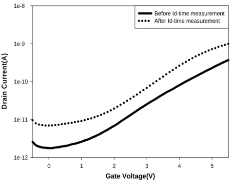
38 Figure 3-6: Id-time measurement performed on a device with 300Å channel. Vg =2.9V and Vd = 0.5V in the test.
...
39 Figure 3-7: Transfer curves of the device tested in Fig.3-6 before and after 60 secondsId-time test.
...
39 Figure 3-8: Transfer curves of a device measured after different stages of the designedexperimental conditions.
...
40 Figure 3-9: Id-time measurements performed on the TFT tested in Fig. 3-8....
40 Figure 3-10: Id-Vg characteristics of the device tested in Fig. 3-8 measured with Vgvaried from 0 to -5.5 V.
...
41 Figure 3-11: The mobile ions (mainly sodium) in the gate oxide were affected by gatebias. Positive gate bias expels ions away from the gate and made
ions toward the gate and results in opposite trend in threshold voltage
shift.
...
41 Figure 3-12: Transfer curves of poly-Si TFTs measured at atmosphere, vacuum, pureN2, and N2 containing 1.5ppm ammonia. The channel thickness is (a)
70Å (b) 300Å, (c) 500Å and (d) 1000Å.
...
42 Figure 3-13: Id-time measurement result of a device with 300Å-thick channel....
44 Figure 3-14: Schematic illustration for the reaction between ammonia and poly-Si....
44 Figure 3-15: Transfer curves of poly-Si TFTs measured at atmosphere, vacuum, pureN2, N2 with 43.2% humidity, and N2 with 43.2% humidity/1.5ppm
ammonia. The channel thickness is (a) 70Å (b) 300Å, (c) 500Å and (d)
1000Å.
...
45 Figure 3-16: Schematic illustration for the reaction between humidity andpoly-Si.
...
47 Figure 3-17: Schematic illustration for the reaction between ammonia/ moisturemixture and poly-Si.
...
47 Figure 3-18: Transfer curves of poly-Si TFTs measured at atmosphere, atmospherewith 1.5 ppm ammonia, and atmosphere again. The channel thickness is
Figure 3-19: The Id-Vg characteristics measured under different ambient conditions.
Chapter 1: Introduction
1.1 Background
There are so many gas species contained in the atmosphere we live in. Some of
them are vital to life, such as oxygen and humidity that should be kept in adequate
level, but some are harmful to human, such as carbon monoxide, nitrogen oxides,
methane, etc. In many working environments, poisonous gases are used for various
kinds of reasons, and incidents caused by leakage of those gases are always a serious
concern. As a result, the development of variable gas sensor technology, especially for
monitoring of polluting and harmful gases such as ozone [1], HCl [2], hydrocarbons
[3], CO [4], H2S [5], NH3 [6], has attracted considerable attention,
There has been a variety of gas sensors proposed and developed so far. A real
sensor era has started in 1970s during which semiconductor combustible gas sensors,
solid electrolyte oxygen sensors, and humidity sensors were commercialized for
non-professional uses. Now there are three types of solid state gas sensors used
widely, namely, solid electrolyte sensors, catalytic sensors, and semiconducting oxide
gas sensors [7].
(i) Solid electrolyte sensors:
1899 [7]. The solid electrolyte’s function is to separate two regions of distinct activity
of the species to be monitored and to allow high mobility of an ion of that species
between the two regions [7]. The sensor’s function is addressed through
measurements of potential, current or charge passed and as a result the ionic
conductivity of the electrolyte must be high, while other modes of electrical
conductivity tend to zero.
Solid electrolyte sensors have been classified into three types by Weppner [8].
They are based on whether the ionic species gotten away from the gas to be detected
coincides with the mobile ion (Type I), the immobile ion (Type II), or neither of them
(Type III) of the solid electrolyte used, as shown in Figure 1-1 [9].
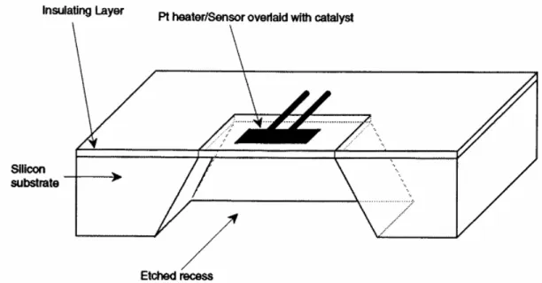
(ii) Catalytic sensors:
Catalytic sensors have been widely used for detection of explosive and flammable
gases and vapors in environment since they were patented in 1962. [10] The devices
are often called “pellistor”. Two typical structures are shown in Figure 1-2 [11] and
Figure 1-3 [7].
The device consists of a catalytic surface which is close to a temperature sensor,
and a heater that keeps the catalyst at a temperature that is high enough to make rapid
combustion of any flammable gas molecules. The heating and temperature
embedded in a refractory bead of alumina which is maintained at 500℃ by a current
going through the wire. The sensor perceives gas concentrations by measuring the
alterations in the resistance of the wire due to temperature increases caused by
combustion.
(iii) Semiconducting oxide gas sensors:
There are numerous materials that have been used in metal oxide sensors, including
both single- (e.g., ZnO, SnO2, WO3, TiO2, and Fe2O3) and multi-component oxides
(BiFeO3, MgAl2O4, SrTiO3, and Sr1-yCayFeO3-x) [12]. The mechanism of gas
detection in these materials is mainly based on the change in the concentration of
adsorbed oxygen occurring at the sensor surface. [13] Oxygen ions adsorb onto the
surface of material, taking electrons away from the bulk and producing a potential
barrier that restricts the movement and conductivity of electrons. When reactive gases,
the targets to be detected, combine with this oxygen, the barrier is lowered and then
the conductivity is increased. As a result, the change of conductivity is related to the
amount of a specific gas in the environment.
However, early application of metal–oxide–semiconductor (MOS) transistors as
gas sensor is to detect hydrogen. The hydrogen absorbs on the surface of the metal
gate and dissociates into hydrogen atoms. And then they diffuse through the gate
interface and lower the height of the energy barrier between the metal and the oxide.
This change of barrier height is reflected in a change of threshold voltage or flat band
potential.
Later amorphous silicon thin-film transistors (TFTs) with a palladium gate show
electrical characteristics suitable for hydrogen sensing. Ammonia can also be detected
using a MOS transistor with a platinum gate.
1.2 Motivation
The use of poly-silicon nano-wire as bio-sensor has been investigated before [14].
However, few works were done for detecting the gases. Nano-wire is a kind of
one-dimensional (1D) structure. This motivates us to carry out this study on
investigating the electrical characteristics of poly-silicon thin-film transistor measured
in different environments. We would also like to explore and distinguish the
difference in the response to sensing the target gas using two-dimensional (2D) planar
structure and one-dimensional (1D) nano-wire test structures.
It is believed that hydrogen affects the electrical characteristics of poly-Si devices
[14]. Hydrogen plasma treatment has been demonstrated to passivate the defects
contained in the poly-silicon [15] and improve device characteristics such as
subthreshold swing, carrier mobility, and saturation drain current. Recently we have
with varying ammonia concentration. This observation encourages us to execute
further experiments on devices with various structural parameters and different
ambient situation to more deeply understand the sensing mechanism.
1.3 Organization of this Thesis
Besides this chapter, this thesis is divided into the following chapters.
In Chap. 2, we describe the process flow of fabricating the n-chanel poly-silicon
TFTs. Also we present the measurement setup.
In Chap. 3, we show the response of poly-silicon TFT gas sensors to the
environments with various pressure and/or various gas compositions. The change of
electrical characteristics to different environments and the effect of structural
parameters are recorded and discussed. Results of nano-wire gas sensors are also
presented and addressed.
Finally, we conclude this thesis in Chap. 4 by summarizing the experimental results
Chapter 2:
Device Fabrication and Measurement Setup
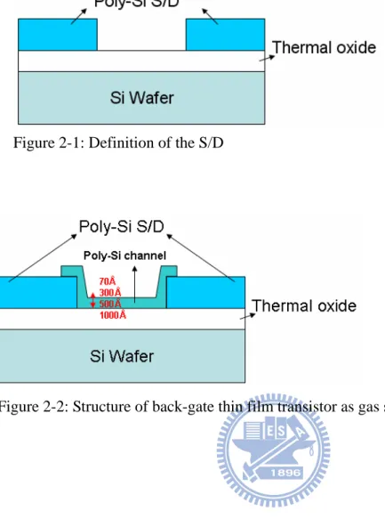
2.1 Fabrication of Planar Poly-Si TFTs
The poly-silicon TFT gas sensors were fabricated on 6-inch p-type (100) Si wafers
with resistivity of 15~25Ω-cm and the thickness of 655~695μm. Note that the
wafers will serve as the back-gate of the completed devices. A wet oxide layer with
thickness of 500 Å serving as gate dielectric first grew on poly-silicon wafer. And
then a poly-Si layer with thickness of 1000 Å was deposited on the wet oxide. The
poly-Si was heavily doped with P+ at energy of 15 keV and dose of 5x10¹⁵ /cm2.
Afterwards, source/drain (S/D) photoresist patterns were formed on the poly-Si layer
by a standard lithography step, followed by a plasma etch step to form S/D (Figure
2-1). Second poly-Si layer was subsequently deposited on the wafer to serve as the
channel layer. In the fabrication, the poly-Si layers were deposited twice to form the
S/D and channel separately, so the thickness of the channel can be modulated flexibly.
In this regard, 4 different channel thicknesses, namely, 70 Å, 300 Å, 500 Å, 1000 Å,
were explored in this work. Channel pattern was then formed with another standard
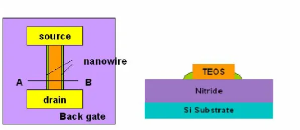
2.2 Nano-wire Gas Sensor Device Structures and Fabrication [16]
The nano-wire field effect transistors (NWFETs) were also fabricated on 6-inchp-type wafers capped with a nitride layer. Figure 2-3(a) and (b) show the top (layout)
and cross-sectional views (along the A – B direction in Figure 2-3(a)), respectively, of
the device, dubbed as device A.
As shown in Figure 2-3, the Si wafers were first capped with a 100 nm-thick nitride
layer. Then, a 100nm-thick oxide layer was deposited by LPCVD. After deposition of
the oxide layer, standard photolithographic and etch steps were employed to form the
oxide dummy structures. Subsequently, a 100 nm-thick amorphous-Si layer was
deposited and then annealed at 600°C for 24 hours in N2 ambient to transform it into
poly-Si. Afterwards, the source/drain (S/D) was doped with phosphorus ion
implantation with a dose of 5E15 cm-2. After the generation of S/D photoresist
patterns with a lithographic step, a reactive plasma etching step was performed to
form the S/D regions. Using the anisotropic sidewall-spacer etching process, poly-Si
NW channels were formed at the sidewalls of the oxide dummy structures during the
S/D etching step. By precisely controlling the etching time, the cross-sectional
dimensions of poly-Si NW channels could be scaled down to sub-100 nm scale.
Subsequently, all devices were then covered with a 200-nm-thick TEOS oxide
process. Note that in the etching steps the wet etching rate of TEOS oxide should be
carefully adjusted so that an oxide layer would remain on source/drain regions while
the channels were exposed. This would prevent the conduction from source to drain
via the test solution.
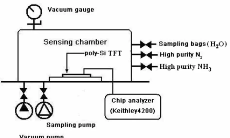
2.3 Gas Sensing Measurements
The electrical characteristics of devices were measured in different environmental
conditions (pressure and composition), including vacuum (2x10⁻¹ torr), nitrogen,
ammonia, steam, mixture of ammonia and nitrogen, mixture of nitrogen and steam,
and so on. For this purpose, a measurement system schematically shown in Figure 2-4
was constructed. In the system a closed chamber is used to house the test devices. A
pump connected to the chamber is used to pump out the air in the chamber and the
pressure as low as 2x10⁻¹ torr can be achieved. After pumping, various gases (nitrogen,
ammonia, and steam) can be injected into the chamber to vary the chamber gas
composition. Note that nitrogen and ammonia are stored in the steel cylinders, while
the steam (vaporized H2O) is stored in sampling bags. Flow of the gases is controlled
by valves. The electrical characteristics are measured by Keithley4200 with setup
measurement software, Interactive Characterization Software (ICS). This
Department of Biological Science and Technology, National Chiao Tung University.
In this study, Id-Vg and Id-time measurements were constantly performed. For the
Id-Vg measurements, Vd was fixed at 0.5 V while Vg was kept at low values in order
not to cause stability and reliability issues on the test devices. For the Id-time
measurements, first we probed the basic electrical characteristics of the device and
chose an appropriate gate voltage in the subthreshold region to ensure obvious change
if the varied environment indeed affects the device. In the process the drain voltage
was also kept at 0.5 volt.
Some major parameters of the transistors, including threshold voltage (Vth) and
subthreshold swing (SS), are defined below [17].
The threshold voltage:
Vth = VFB – (Qd+qD)Cox + 2ΦF (2-1).
In the expression, Qd (Coul/cm2) is the effective charge stored in the depletion region
of channel when MOSEFT is turned on, Cox is the capacitance of gate oxide per unit
area, D is the doping concentration of the channel, and VFB is the flat-band voltage
with the following relation:
VFB =ΦMS – Qi/Cox (2-2), ΦMS =ΦM -ΦS, (2-2a), where ΦM is the work function of gate material ,ΦS is the work function of the
channel material, and Qi is the charge in oxide that includes mobile ions, trapped
charge, fixed charge, and charge in interface of oxide and silicon. ΦF is the silicon
bulk potential:
ΦF = ln(p/ni) x (kT /q) = ln(ni/n) x (kT/q),
where kT/q is thermal energy, k is Boltzmann constant, T is absolute temperature, q is
the electron charge, p is the concentration of holes at thermal equilibrium, n is the
concentration of electrons at thermal equilibrium, and ni is the intrinsic concentration
of electrons and holes.
The on-current in the linear region (Vg > Vth, Vg-Vth > Vd ) can be expressed as
Id = μCox x (W/L) x [(Vg - Vth) x Vd – Vd2/2] (2-3),
where μ is the carrier mobility, W is the channel width, and L is the channel length.
The on-current in the saturation region (Vg > Vth, Vg-Vth < Vd ) can be expressed
as :
Id = μCox x (W/L) x (Vg - Vth)2 x 1/2 (2-4).
Definition of subthreshold swing (SS) is :
(2-5).
Chapter 3 Electrical Characteristics of Back-Gate TFT Gas
Sensor
3.1 Basic Electrical Characteristics of Devices with Different Channel
Structure under Atmosphere
The electrical characteristics of NWFET and back-gated planar TFTs with channel
thickness: 70Å, 300Å, 500Å and 1000Å are shown in Figure 3-1. The measurements
were done under atmosphere and at room temperature. For the planar devices the
drain current increases with increasing channel thickness in general. The device with
70Å channel thickness exhibits the lowest on and off current. This phenomenon is
attributed to the high resistance of the ultra-thin channel. However, the device with
70Å thickness channel also depicts slightly better subthreshold swing (SS) over the
remaining planar devices. This implies that device with thinner channel has better
gate controllability.
By comparing the transfer characteristics of NWTFT with those of the planar
devices, as shown in Figure 3-1, clearly the NWFET exhibits much improved
Part of the improvement can be attributed to nanowire’s high surface/volume ratio.
However, some hydrogen species are suspected to have been contained in the poly-Si.
These H species come from the underlying SiN (see Figure 2-3) which was deposited
with H-related reaction gas (e.g., SiH4 and NH3), thus abundant of hydrogen atoms
are incorporated in the SiN film [18]. Portion of the H species diffuse into the poly-Si
nanowire and passivate the defects existing therein in the subsequent process steps,
thus the device shows improved performance.
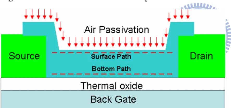
We can speculate reasonably that there is a conducting path from the source to
drain near the film surface (Figure 3-2) in addition to the nominal conduction channel
manipulated by the back gate near the oxide/film interface. The surface conduction
path is significantly affected by the environment as there is no dielectric passivation,
and less affected by the back gate unless the channel film is sufficiently thin. Below
are the results of a series of experiments carried out to examine the above postulation.
3.2 The Effects of Measurement Environment on Poly-Si TFTs
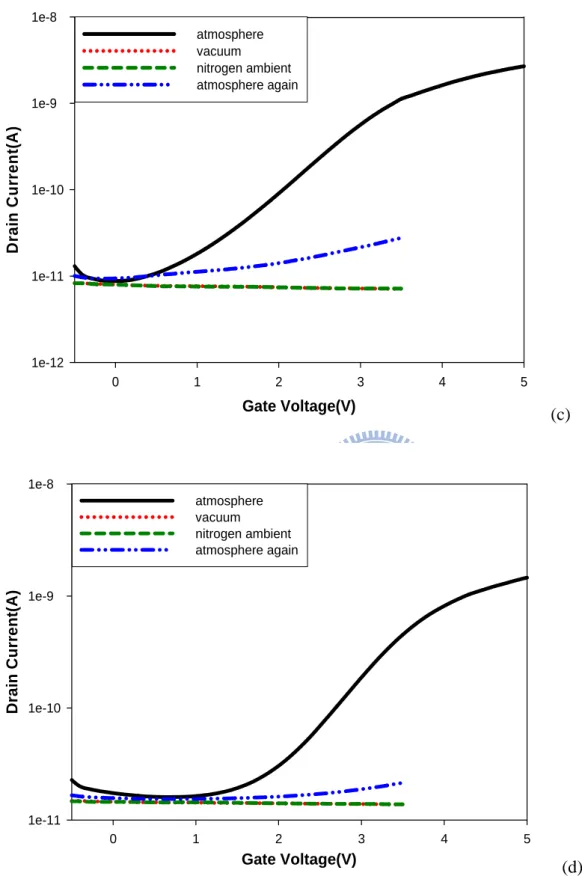
3.2.1 Device Characteristics in Vacuum and in Nitrogen Ambient
Typical characteristics of the planar TFTs with various film thickness measured
measurements, the device was first tested in normal ambient which had a moisture
level of 42%, and then in the closed test chamber (see the description in Chap. 2)
which was pumped down to 0.2 Torr. After the second measurement performed in
vacuum, the vacuum chamber was injected with high purity N2 (99.999%) to increase
the pressure to around 1 atm, and then the third measurement was performed. Finally
the chamber was open to expose the device to the air again. We then repeated the
measurements to check if the transfer characteristics of the device recovered to the
original characteristics.
In the figures we can find that there is a big change in the Id-Vg curves as the test
environment is switched from atmosphere to vacuum. When measured in vacuum, the
drain current became low and insensitive to the variation of gate voltage. As N2 was
injected into the chamber, the Id-Vg curve remained the same as that measured in
vacuum.
When the device was put back to the normal air, the I-V characteristics would
recover, but the extent depended strongly on the film thickness. As can be seen in
Figure 3-3(a), the TFT with 70Å-thick channel almost return to the original
characteristics while the other devices with thicker channel do not t recover
completely (Figures 3-3(b) ~3-3(d)).
normal air which has a relative humidity of 42 %. Thus we postulate that the above
difference in I-V characteristics is due to the existence of moisture and the interaction
between moisture and the poly-Si films. Note the moisture contains H-related species
(such as H or OH) which can help passivate the defects contained in the poly-Si [19].
The schematic illustration about the passivation of defects in the grain boundaries
with H from the moisture in the ambient is shown in Figure 3-4 (a). In the figure and
following discussion, for simplicity, we assume H is the main species responsible for
the passivation of the defects. Note that the fresh devices should contain specific
amount of H throughout the film since the last step in device fabrication was a
de-ionized water rinse after the removal of photoresist with H2SO4/H2O2. According
to the water passivation effect [14], some H species should remain in the films even
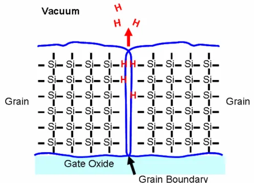
when the device was dried. At vacuum, the amount of active defects in the poly-Si
increases because the vacuum tends to drive out the H from the grain boundaries and
destruct the bonding, such as Si-H, leaving the defects unpassivated (see Figure 3-4).
The amount of dangling bonds increases massively and affects the electrical
characteristics considerably. As the high-purity N2 is injected into the chamber such
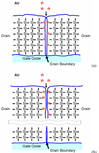
characteristics are retained due to the dry ambient. After returning to the air, the Id-Vg
curve is restored due to the diffusion of H from the moisture contained in the normal
diffusion process. The device with70 Å-thick channel restores soon due to its shallow
channel (Figure 3-5(a)). However, for devices with thicker channel it needs longer
time to recover completely. The gated channel (bottom path shown in Figure 3-2) thus
retains a high amount of un-passivated defects, as shown in Figure 3-5(b). This
explains why the characteristics cannot recover completely in Figures 3-3(b)~(d) as
the test environment returns to the normal air.
3.2.2 Id-time Measurements
In this Id-time measurement, the setup of measurement environment is the same
as that described in last sub-section. The measurement scheme is stated in Sec. 2.3,
and the Vg is set at 0.5V. In Figure 3-6, the Id of a TFT with 300Å channel thickness
initially increased as measured under normal atmosphere. To check this phenomenon
we compared the transfer curves of the device before and 60 sec after the above
Id-time measurement. The results are shown in Figure 3-7. We can see that the
threshold voltage becomes smaller while the SS remains unchanged after the Id-time
measurement. To confirm and figure out the mechanism, we made a series of
measurements performed on one another device with the results are shown in Figure
3-8. First, we measured the transfer curve of the device with 300Å channel thickness
measurement (Vg = 3.7V > 0V ) (curve (1) in Figure 3-9) on the device for 2100 sec,
and then the transfer curve was measured again (curve (2) in Figure 3-8). As the trend
shown in Figure 3-7, the threshold voltage of the curve (2) in Figure 3-8 shifts
leftward. And then we made Id-Vg measurement with gate voltage sweeping from 0
to -5V, as shown in Figure 3-10. After that we measured the curve 3) in Figure 3-8
and found the threshold voltage shifts slightly rightward with respect to the curve (2)
shown in the same figure. Before measuring the curve (4) in Figure 3-8, we made
another Id-Time measurement with Vg=-3.7V (< 0V) (curve (2) in Figure 3-9). The
curve (4) shifts leftward and becomes close to the original curve (1) in Figure 3-8.
From the above experimental results we postulate the instability in the transfer
curves of the test devices as measured in the normal ambient is due to the action of
mobile ions, like sodium or potassium ions, presenting in the oxide. This is a well
known issue for old MOSFET technology [20]. Since there is no passivation dielectric
covering the devices, these contamination species are likely to appear in the test
samples. As a positive gate voltage is applied for a sufficient long time, these ions
tend to accumulate near the oxide/channel interface and the threshold voltage is thus
decreased (see Figure 3-11(a)). In opposite situation as the gate bias is negative, these
ions would be attracted toward and accumulate near the oxide/gate interface, leading
Now let’s return to discuss the results shown in Figure 3-6. While the air was
pumped out to vacuum the text chamber, the Id dropped drastically which is
consistent with the results shown in Figure 3-3(b). After the measurement
environment turned back to atmosphere, the current increased again. The air has
obvious passivation to the device.
3.3 Effects of Ammonia
In this experiment, the device was first tested in normal ambient. Then the
device was put into the chamber and the chamber was pumped down to 0.2 Torr.
After the second measurement performed in vacuum, the nitrogen was injected into
the chamber to increase the pressure to 1 atm, and then the third measurement was
performed. Afterwards, 1.5 ppm ammonia (NH3) was injected into the chamber.
Finally, the fourth measurement was performed.
The results are shown in Figures 3-12(a) to (d) for devices with different channel
thickness. Also the results of Id-time measurement performed on a TFT with 300 Å
channel thickness are shown in Figure 3-13. Basically the results shown in Figures
3-12(a)~(d) are the same as those shown in Figures 3-3(a)~(d) at the first three stages
measured in normal air, vacuum, and N2 ambient. As the ammonia is introduced, no
channel thickness. Figure 3-13 also shows similar trend. The observation implies the
1.5 ppm ammonia does not result in significant passivation effect as the moisture does
to recover the device characteristics.
In [21] it was mentioned that ammonia (NH3) might dissociatively absorb at 300
K to form SiH and SiNH2 on the surface of Si, as shown in Figure 3-14. Though slow
thermal decomposition of NH2 to N and H2 occurs even at 320 K, most Si-NH2 is
stable up to 630 K [22]. However, owing to the trace amount of NH3 presenting in the
ambient, these H-related species cannot exhibit significant passivation effect on the
device characteristics.
3.4 Effects of Moisture and Moisture/Ammonia Mixture
Here we first examined the response of device characteristics to the injection of
moisture and ammonia. In this test the former three stages of measurements were the
same as those described in former section. Then the humidity was injected into the
chamber until the moisture content in the chamber reached 42.6 % and the fourth
measurement was performed. Finally, 1.5 ppm ammonia was injected into the
chamber before the fifth measurement was performed.
The results are shown in Figures 3-15(a)~(d) for devices with different channel
sections, here we just discuss the effect of moisture and moisture/NH3 mixture. As
can be seen in the figures, the input of moisture can indeed improve the device
characteristics. In [23], it was mentioned that in a H2O molecule the oxygen end tends
to bond with a Si-Si dimmer on Si surface, whereas the hydrogen ends tend to attach
to dangling bonds within the neighboring row of dimmers. The bindings, Si-H and
Si-OH, can passivate the defects in poly-Si (Figure 3-16). However, as mentioned
above, such passivation is limited to the region closest to the surface of poly-Si,
therefore the characteristics cannot fully recover.
One interesting phenomenon observed in Figures 3-15(a)~(d) is the dramatic
increase in the drain current as the ammonia is mixed with the steam in the
environment. In [24], the extent of the hydrolytic reaction in wet ammonia: H2O +
NH3 -> NH4+ + OH-, was mentioned (Figure 3-17). Formation of NH4+ can get more
OH- dissociated from H2O and thus the passivation effect can be greatly enhanced as
compared with ammonia or moisture alone.
However, some remarks on the effect should be given. First, the dependence
between the extent of drain current enhancement and the channel thickness is not the
same as that illustrated in Figures 3-3(a)~(d). From Figure 3-15(d), the characteristics
measured under moisture/ammonia mixture have higher off-current than the original
transfer curves. It is obvious that most of the conduction current pass through near the
top surface of channel (Figure 3-2) and thus weaken the controllability of back-gate.
From this observation, we conclude that the passivation mechanism of
moisture/ammonia mixture mainly occurs in the top surface region of the poly-Si
channels.
Next we investigate the interaction of ammonia with the moisture in the normal
air and the resultant impact on device performance. In the testing of Figure 3-18, we
made first device measurement under atmosphere. After closing the test chamber we
injected ammonia into the chamber directly without vacuum process and then
performed the second measurement. Finally we opened the chamber and made the
third measurement after 5 min the ammonia dispersed away from the chamber (5
minutes later from opening the chamber).
In Figures 3-18(a)~(d), as NH3 is injected, not only the Vth but also the SS
reduces dramatically, unlike the situation shown in Figures 3-15(a)~(d). As mentioned
in Sec. 3.1, the fresh devices contain an amount of H-related species. It is speculated
that those H-related species could accelerate the penetration of ammonia and thus the
passivation is not restricted to the regions near the surface. In other words, the region
close to the oxide/channel interface is also passivated by the ammonia even when the
air reacts with ammonia and results in the enhancement of defect passivation. For the
present case, we speculate that trace amount of H2O molecules may contain inside the
channel of the fresh devices, and are most likely located in the grain boundaries. The
ammonia presenting in the environment may penetrate into the channel film via the
grain boundaries and react therein with the H2O molecules, resulting in the enhanced
passivation in the region near the oxide/channel interface and the improved SS.
Another interesting finding shown in the figures is that, when the ammonia
disperses away from the chamber, both threshold voltage and SS increase. This
indicates that the above passivation mechanism is not stable and can’t retain. More
effort is certainly needed for deeper understanding of this phenomenon.
3.5 The Effect of Measurement Environment on Poly-Si Nano-wire
Transistors
The above analysis used planar poly-Si TFTs as the test vehicle and the results
indicate the interaction between the poly-Si and the environment plays an important
role. This implies that the poly-Si nanowire devices should have higher response to
the change of environment owing to the nanostructure. Below are the experimental
results for examination of such speculation.
The measurement results on poly-Si nanowire transistor are shown in Figure 3-19.
e.g., Figures 3-3(a)~(d), 3-15(a)~(d), 3-12(a)~(d), and 3-18(a)~(d). However, it should
be noted that the measurements performed in Figure 3-19 were done with a narrow
Vg range (0~2V) and the Vg is low. Despite the low Vg, the on/off current ratio is
high, indicating that a high sensitivity can indeed be obtained with the poly-Si NW
Chapter 4: Conclusion and Future Work
4.1 Conclusion
This thesis presents the fabrication of planar and NW poly-silicon TFTs having
channel exposing to the environment, and studies the characteristics of the devices
under different measurement environment. The NW devices exhibit much improved
performance than the planar counterparts. In addition to the adoption of the NW
structure, the effect of nitride layer underlying the poly-silicon NW is also identified
as one of the reasons responsible for such improvement.
The electrical characteristics of Id-time measurements have been investigated. Also
the electrical characteristics of the fabricated devices are characterized under various
ambient conditions. One of the most interesting findings is that, under vacuum
environment, the device characteristics is significantly degraded in terms of dramatic
increases in SS and Vth. As the environment returns to the normal air, the device
characteristics may recover but the extent depends on the film thickness. A model
proposed to describe the interaction between the poly-Si films and the environment.
Effects of moisture and ammonia are also investigated. The results validate the
feasibility of poly-Si-based devices for gas sensing applications.
4.2 Future work
First, the feasibility of using poly-Si devices for sensing many various types of
gases should be investigated, such as the gas with (i.e., carbon monoxide) or without
(i.e., methane) chemical polarity. The difference between the measurement of gas with
or without chemical polarity would reveal useful information. Certain surface
treatments should also be explored to see if they are useful for enhancing the
sensitivity.
Some unclear points remained in the thesis need further efforts to address. For
example, in Sec. 3.4, the recovery of the electrical characteristics after the ammonia
was dispersed away. Passivation of defects with ammonia is obviously not stable. To
further investigate this phenomenon, some instruments such as Fourier transform
infrared transmission spectroscopy (FTIR) would be useful to understand the surface
composition of poly-silicon channel as the device is exposed to the gas. Thermal
desorption spectroscopy (TDS) technique is also suggested to explore the desorbed
References
[1] J. P. Lodge, “Methods of Air Sampling and Analysis,” 3rd ed., Chelsea, MI:
Lewis, 1989.
[2] K. Nakagawa, T. Kitagawa and Y. Sadaoka, “An Optochemical HCl Gas Using
5,10,15,20-tetrakis(3’,5’-di-tert-butyl, 4’-hydroxyphenyl) Porphin-ethylecllulose
Composite Films,” Sens. Actuators B, Vol. 52, Issues 1-2, 1998, pp. 10–14.
[3] D. D. Lee and D. H. Choi, “Thick Film Hydrocarbon Gas Sensors”, Sens.
Actuators B,” Vol. 1, Issues 1-6, 1990, pp. 231–235.
[4] M. Nitta and M. Haradome, “Oscillation Phenomenon in Thin-film CO Sensor,”
IEEE Trans. Electron Devices, Vol. ED-26, Issue 3, 1979, pp. 219–223.
[5] R. Lalauze, N. Bui and C. Pijolat, “Interpretation of the Electrical Properties of a
SnO2 Gas Sensor after Treatment with Sulfur Dioxide,” Sens. Actuators, Vol. 6,
1984, pp. 119–125.
[6] G. S. V. Coles, K. J. Gallagher and J. Watson, “Fabrication and Preliminary
Results on Tin(IV)-oxide-based Gas Sensors,” Sens. Actuators, Vol. 7, 1985, pp.
89–89.
[7] P. T. Moseley, “Review Article Solid State Gas Sensors,” Meas. Sci. Technol.,
Vol. 8, 1997, pp. 223–237.
[8] W. Weppner, “Solid State Electrochemical Gas Sensors,” in Proc. 2nd Int.
[9] Duk-Dong Lee and Dae-Sik Lee, “Environmental Gas Sensors,” IEEE Sensors
Journal, Vol. 1, No. 3, 2001, pp. 214-224.
[10] A. R. Baker, “Combustible Gas Detecting, Electrically Heated Element,”
U.K. Patent 892 530, 1962.
[11] James B. Miller, “Catalytic Sensors for Monitoring Explosive Atmospheres,”
IEEE Sensors Journal, Vol. 1, No.1, 2001, pp. 88-93.
[12] B. Hoffheins, “Solid State, Resistive Gas Sensors,” in Handbook of Chemical
and Biological Sensors, R.F. Taylor and J.S. Schultz, eds., Philadelphia: Institute
of Physics, 1996.
[13] Stephanie A. Hooker, “Nanotechnology Advantages Applied to Gas Sensor
Development,” The Nanoparticles 2002 Conference Proceedings, pp. 1-7.
[14] Horng-Chih Lin, Chun-Jung Su, Cheng-Yun Hsiao, Yuh-Shyong Yang and
Tiao-Yuan Huang, “Water Passivation Effect on Polycrystalline Silicon
Nanowires,” Applied Physics Letters, Vol 91, 202113, 2007.
[15] T. I. Kamins and P. J. Marcoux, “Hydrogenation of Transistors Fabricated in
Polycrystalline-Silicon Films,” IEEE Electron Device Letters, Vol. EDL-1, 1980,
pp. 159-161.
[16] Jo-Fen Wei, “Fabrication Process and its Effects on the Electric Characteristics of
Master Thesis, Department of Biological Science and Technology, National
Chiao Tung University, 2009.
[17] S. M. Sze and Kwok K. Ng, ”Physics of Semiconductor Devices,” Third Edition,
John Wiley & Sons, 2007.
[18] Chia-Yu Lu, “A Study of Drive Current Enhancement Methods and Related
Reliability Issues for MOSFETs,” PhD. Dissertation, Department of Electronics
Engineering & Institute of Electronics, National Chiao Tung University, 2006.
[19] C. G. Van de Walle and R. A. Street, “Silicon-hydrogen Bonding and Hydrogen
Diffusion in Amorphous Silicon,” Materials Research Society Symposium
Proceedings: Amorphous Silicon Technology, 1995, San Francisco, CA.
Pittsburg, PA: Materials Research Society, pp. 377-389.
[20] Ben G. Streetman and Sanjay Banerjee, “Solid State Electronic Devices,” 5th
Edition, Prentice Hall, 2000.
[21] F. Bozso and P. Avouris, “Reaction of Si(100) with NH3 : Rate-Limiting Steps
and Reactivity Enhancement via Electronic Excitation,” Physical Review Letters,
Vol. 57, 1986, pp. 1185-1188.
[22] X. -L. Zhou, C. R. Floresl and J. M. White, “Decomposition of NH3 on Si(100): a
SSIMS Study,” Surface Science, Vol. 268, Issues 1-3, 1992, Pages L267-L273.
Electron-energy-loss and Photoemission Spectroscopies,” Physical Review B,
Vol. 33, Issues 6, 1986, pp. 4233-4236.
[24] Robert R. Dewald and Richard V. Tsin, “Reaction of the Solvated Electron with
Water in Liquid Ammonia,” Chemical Communications, No. 13, 1967, pp.
Figure 1-2: Pellistor: catalytic bead detector element.
Figure 2-1: Definition of the S/D
Figure 2-3: NWTFT (a) Top and (b) cross-sectional view of poly-Si NWFET with the stacked dielectric nitride layer. These NWTFT devices were offered by Jo-Fen Wei.
Figure 2-4: The measurement system for probing electrical characteristics of the test devices: The steam (vaporized H2O) is stored in the sampling bag. The nitrogen and ammonia are stored in the steel cylinder. Flow of the gases is controlled by a valve. Figure 2-4 was offered by Yuan-ren Lo.
Gate Voltage(V) 0 1 2 3 4 5 Dr a in Cu rr e n t( A) 1e-13 1e-12 1e-11 1e-10 1e-9 1e-8 1e-7 1e-6
70A channel thickness TFT 300A channel thickness TFT 500A channel thickness TFT 1000A channel thickness TFT NW FET
Figure 3-1: Transfer characteristics of planar devices with different channel thickness and a NW device.
Gate Voltage(V) 0 1 2 3 4 5 Dr a in Cu rr en t( A ) 1e-13 1e-12 1e-11 1e-10 1e-9 atmosphere vacuum(2x10^-1 torr) nitrogen ambient atmosphere again (a) Gate Voltage(V) 0 1 2 3 4 5 D rai n C ur re nt (A ) 1e-12 1e-11 1e-10 1e-9 atmosphere vacuum(2x10^-1 torr) nitrogen ambient atmosphere again (b)
Gate Voltage(V) 0 1 2 3 4 5 Dr a in Cu rr e n t( A) 1e-12 1e-11 1e-10 1e-9 1e-8 atmosphere vacuum nitrogen ambient atmosphere again (c) Gate Voltage(V) 0 1 2 3 4 5 Dr ai n Cur ren t( A ) 1e-11 1e-10 1e-9 1e-8 atmosphere vacuum nitrogen ambient atmosphere again (d)
Figure 3-3: Transfer curves of poly-Si TFTs measured at atmosphere, vacuum, N2, and atmosphere again. The channel thickness is (a) 70Å (b) 300Å, (c) 500Å and (d) 1000Å.
Figure 3-4: Schematic illustration showing the outgas of hydrogen from the grain boundaries of poly-Si due to the pressure difference.
(a)
(b)
Figure 3-5: (a) When returning to the normal air from vacuum, the H-related species diffuse from the moisture in the air to the poly-Si through the grain boundaries and may passivate the defects therein. (b) As the poly-Si film is thick, the deeper part of the film receives less passivation due to diffusion mechanism.
Figure 3-6: Id-time measurement performed on a device with 300 Å channel. Vg = 2.9V and Vd = 0.5V in the test. Gate Voltage(V) 0 1 2 3 4 5 D rai n C u rr en t( A ) 1e-12 1e-11 1e-10 1e-9 1e-8
Before Id-time measurement After Id-time measurement
Figure 3-7: Transfer curves of the device tested in Fig.3-6 before and after 60 seconds Id-time test.
Gate Voltage(V) 0 1 2 3 4 5 Dr a in Cu rr e n t( A) 1e-12 1e-11 1e-10 1e-9
(1):before Id-time measurement
(2):after Id-time measurement(Vg=3.7V, Vd=0.5V) (3):after (2) and Id-Vg(0~-5V) measurement
(4):after (2),(3)and Id-time measurement(Vg=-3.7V, Vd=0.5V)
Figure 3-8: Transfer curves of a device measured after different stages of the designed experimental conditions.
Gate Voltage(V) -5 -4 -3 -2 -1 0 Dr a in Cu rr e n t( A) 1e-12 1e-11 1e-10
Figure 3-10: Id-Vg characteristics of the device tested in Fig. 3-8 measured with Vg varied from 0 to -5.5 V.
Figure 3-11: The mobile ions (mainly sodium) in the gate oxide were affected by gate bias. Positive gate bias expels ions away from the gate and made threshold voltage shift negatively, while negative gate bias attracts the ions toward the gate and results in opposite trend in threshold voltage shift.
Gate Voltage(V) 0 1 2 3 4 5 Dr a in Cu rr e n t( A ) 1e-14 1e-13 1e-12 1e-11 1e-10 1e-9 atmosphere vacuum nitrogen ambient
nitrogen containing 1.5 ppm ammonia
(a) Gate Voltage(V) 0 1 2 3 4 5 Dr ia n Cur re n t( A) 1e-12 1e-11 1e-10 1e-9 atmosphere Vacuum nitrogen ambient
nitrogen containing 1.5 ppm ammonia
Gate Voltage(V) 0 1 2 3 4 5 D rai n C ur rent (A ) 1e-12 1e-11 1e-10 1e-9 1e-8 atmosphere vacuum nitrogen ambient
nitrogen containing 1.5 ppm ammonia
(c) Gate Voltage(V) 0 1 2 3 4 5 D rai n C ur re nt (A ) 1e-11 1e-10 1e-9 1e-8 atmosphere vacuum nitrogen ambient
nitrogen containing 1.5 ppm ammonia
(d)
Figure 3-12: Transfer curves of poly-Si TFTs measured at atmosphere, vacuum, pure N2, and N2 containing 1.5 ppm ammonia. The channel thickness is (a) 70 Å (b) 300 Å, (c) 500 Å and (d) 1000 Å.
Figure 3-13: Id-time measurement result of a device with 300 Å-thick channel.
Gate Voltage(V) 0 1 2 3 4 5 D rain C urre nt(A ) 1e-15 1e-14 1e-13 1e-12 1e-11 1e-10 1e-9 atmosphere vacuum nitrogen ambient
nitrogen with 43.2% humidity
nitrogen with 43.2% humidity/1.5 ppm ammonia
(a) Gate Voltage(V) 0 1 2 3 4 5 D ra in C ur re nt (A ) 1e-12 1e-11 1e-10 1e-9 atmosphere vacuum nitrogen ambient
nitrogen with 43.2% humidity
nitrogen with 43.2% humidity/1.5 ppm ammonia
Gate Voltage(V) 0 1 2 3 4 5 Dr a in Cu rr e n t( A) 1e-11 1e-10 1e-9 1e-8 atmosphere vacuum nitrogen ambient
nitrogen with 43.2% humidity
nitrogen with 43.2% humidity/1.5 ppm ammonia
(c) Gate Voltage(V) 0 1 2 3 4 5 Dr a in Cu rr e n t( A ) 1e-11 1e-10 1e-9 1e-8 atmosphere vacuum nitrogen ambient
nitrogen with 43.2% humidity
nitrogen with 43.2% humidity/1.5 ppm ammonia
(d)
Figure 3-15: Transfer curves of poly-Si TFTs measured at atmosphere, vacuum, pure N2, N2 with 43.2% humidity, and N2 with 43.2% humidity/1.5 ppm ammonia. The channel thickness is (a) 70 Å (b) 300 Å, (c) 500 Å and (d) 1000 Å.
Figure 3-16: Schematic illustration for the reaction between humidity and poly-Si.
Gate Voltage(V) 0 1 2 3 4 5 Dr a in Cu rr e n t( A) 1e-14 1e-13 1e-12 1e-11 1e-10 1e-9 atmosphere
atmosphere with 1.5 ppm ammonia atmosphere again (a) Gate Voltage(V) 0 1 2 3 4 5 D ra in Cu rr e n t( A) 1e-12 1e-11 1e-10 1e-9 1e-8 atmosphere
atmosphere with 1.5 ppm ammonia atmosphere again
Gate Voltage(V) 0 1 2 3 4 5 Dr a in Cur re nt (A) 1e-12 1e-11 1e-10 1e-9 1e-8 atmosphere
atmosphere with 1.5 ppm ammonia atmosphere again (c) Gate Voltage(V) 0 1 2 3 4 5 Dr a in Cu rr e n t( A ) 1e-11 1e-10 1e-9 atmosphere
atmosphere with 1.5 ppm ammonia atmosphere again
(d) Figure 3-18: Transfer curves of poly-Si TFTs measured at atmosphere, atmosphere with 1.5 ppm ammonia, and atmosphere again. The channel thickness is (a) 70 Å (b) 300 Å, (c) 500 Å and (d) 1000 Å.
Gate Voltage(V) 0.0 0.5 1.0 1.5 2.0 1e-12 1e-11 1e-10 1e-9 1e-8 1e-7 1e-6 t(A )
Figure 3-19: The Id-Vg characteristics measured under different ambient conditions. .
Dra in Curre n Air (55%Hum.) air + 0.5ppm NH3 air + 1.5ppm NH3 vacuum nitrogen N2 + 0.5ppm NH3 N2 + 1.5ppm NH3 17.3%Hum. H2O H2O + 0.5ppm NH3 H2O + 1.5ppm NH3
![Figure 1-1: Three types of solid-electrolyte gas sensors [9].](https://thumb-ap.123doks.com/thumbv2/9libinfo/8400514.179198/40.892.140.507.119.823/figure-types-solid-electrolyte-gas-sensors.webp)