國 立 交 通 大 學
光 電 工 程 研 究 所
碩士論文
利用主動層優化降低氮化鎵發光二極體效率下
降特性之研究
Reduction of efficiency droop behavior in InGaN/GaN
light emitting diodes by optimization of active
region
研究生:盧昱昕
指導教授:郭浩中 教授
盧廷昌 教授
利用主動層優化降低氮化鎵發光二極體效率下降特性之研究
Reduction of efficiency droop behavior in InGaN/GaN light emitting
diodes by optimization of active regions
研究生:盧昱昕 Student: Yu-Shin Lu 指導教授:郭浩中 教授 Advisor: Prof. Hao-Chung Kuo
盧廷昌 教授 Prof. Tien-Chang Lu
國 立 交 通 大 學
光電工程研究所
碩 士 論 文
A Thesis
Submitted to Institute of Electro-Optical Engineering
College of Electrical Engineering
National Chiao Tung University
in Partial Fulfillment of the Requirements
for the Degree of
Master
In
Electro-Optical Engineering
July 2010
利用主動層優化改善氮化鎵發光二極體效率下降特性之研究
研究生:盧昱昕 指導教授: 郭浩中教授 盧廷昌教授 國立交通大學光電工程研究所碩士班摘要
本論文中,我們利用改善主動層品質及優化量子井結構等方式,試圖提高氮 化鎵發光二極體於高電流時的發光效率.我們將低溫成長之氮化鎵薄膜置於 n-GaN及主動層間,並將此樣品與一般所使用的InGaN/GaN prestrain layer及未做 任何結構之樣品作比較。並更進一步探討在高載子濃度下的LED發光效率.並用 漸變式量子井結構進一步改善效率隨載子濃度遞減之情況。我們利用光激發螢光 (Photoluminescence, PL)、電激發螢光(Electroluminescence, EL)、以及Advanced Physical Models of Semiconductor Devices (APSYS)模擬軟體等進行樣品的光學與 電特性分析。在本論文中,藉由變強度之光激發螢光實驗我們可以得知有插入prestrain layer 之樣品,當載子濃度提高時,其波長藍移量較小,亦即quantum confined Stark effect (QCSE)較小,因此我們可以得知使用低溫成長之氮化鎵薄膜的確是 放了主動層內部之應力,並藉由室低溫變強度光激發螢光去定義出三塊樣品之內 部量子效率,且有應力釋放之樣品期內部量子效率有明顯提高,並且在高載子濃 度時,使用低溫成長之氮化鎵薄膜樣品之效率遞減情況最為輕微,從半高寬與載 子濃度的相關圖及CL得表面影像中可以得知低溫成長之氮化鎵薄膜有效降低了 主動層內部銦含量分布不均勻之情況,故可以減少載子被非輻射復合中心捕捉之 機率 根據以上的實驗結果,使用低溫成長之氮化鎵薄膜及漸變厚度量子井結構 的確能有效提升發光二極體之特性.分別在電流密度為22 A/cm2 及244 A/cm2 時
Reduction of efficiency droop behavior in InGaN/GaN light emitting
diodes by optimization of active regions
Student :Yu-Hsin Lu Advisor: Prof. Hao-Chung Kuo Prof. Tien-Chang Lu
Institute of Electro-Optical Engineering
National Chiao Tung University
Abstract
Direct wide-bandgap gallium nitride (GaN) and other III-nitride-based semiconductors have attracted much attention for potential applications such as blue, green, and ultraviolet (UV) light-emitting diodes (LEDs) and blue laser diodes (LDs). Although InGaN-based LEDs have many excellent properties, the efficiency droop will occur under high current injection, resulting in the application of lighting was limited. In order to reduce the efficiency droop behavior in InGaN/GaN light emitting diodes, several semiconductor technologies have been used, such as non-polar material, AlInGaN barrier layer, thick DH active region or thick QW, barrier doping etc..
In this study, we tried to reduce the efficiency droop behavior in InGaN-based by using low temperature GaN (LT-GaN) pre-strained layer and graded quantum well (GQW) in which the well-thickness increases along [0001] direction. To better understand the influence of LT-GaN pre-strained layer and GQW on efficiency droop, a lot of measurement techniques were performed to investigate the optical and electrical properties of the grown specimens, including photoluminescence (PL), cathodoluminescence (CL), electroluminescence (EL), L-I-V curve and Advanced Physical Models of Semiconductor Devices (APSYS). Form power-dependent PL
layer and GQW exhibited relatively slight blue shift, which could be related to smaller quantum confined Stark effect (QCSE). Besides, the CL images shown that the specimen has more uniform emission area and less dark spots, resulting in the enhancement in emission efficiency. APSYS simulation analyzed that specimen with LT-GaN pre-strained layer and GQW revealed superior hole distribution as well as radiative recombination distribution. Additionally, according to the analysis of electroluminescence spectrum, specimen with LT-GaN pre-strained layer and GQW reveals additional emission peak from the following narrower wells within GQWs. These results are in good agreement with the result obtained from APSYS simulation.
Based on the results mentioned above, a high-efficiency InGaN-based LED with LT-GaN pre-strained layer and GQW has been fabricated, which demonstrated an improvement in output power of 36% at current density of 22 A/cm2 and 71% at current density of 244 A/cm2. Besides, the efficiency droop was alleviated to be about 17% from maximum at current density of 22 A/cm2 to 244 A/cm2, which is much smaller than 54% of conventional LED.
誌謝
經過兩年的研究生涯,終於要在這階段告一段落了。直到現在,才有一點 即將要畢業的感覺。這段日子裡所學到的東西太多了,不僅僅是學術研究上的知 識,也包含了為人處事的態度,我要感謝那些在這兩年所有幫助我成長的人。 在我遇到問題時不吝幫我解答,使我可以順利的完成我的碩士學位。 首先,我由衷的感謝王興宗老師的指導,老師做學問認真的態度以及爽朗的 笑聲深深地影響我;感謝郭浩中老師在我實驗上遭遇困難時,給予我幫助,以及 感謝老師平時對我的鼓勵,使我遇到挫折時能更勇敢的面對;感謝盧廷昌老師的 指導,使我能夠有許多想法去解決實驗上所遇到的問題。 感謝清華學長,平常Meeting上的指導以及對研究上的規劃和叮嚀,每當我 開始怠惰,總是有學長在旁邊鞭策,以及研究上給予的幫助;感謝李博學長,我 總是向你詢問許多磊晶及材料上的問題,每次你都不厭其煩的幫助我,也不時會 對於實驗上提供不少想法,因為你和清華學長的協助,我才能更順利的完成我的 實驗。感謝世邦學長和鏡學學長,有你們的幫助我才能得到穩定的樣品完成研 究。感謝小科學長,謝謝你在我碩一時教我熟習實驗的一切架構以及許多LED的 基礎知識;感謝Joseph、阿飛、David、dopin、阿翔、依嚀、祥淇、永吉、惟雯、 哭哭、小胖、小邱、彥群 等碩二的同學,因為你們而讓我的碩士生活更多采多 姿,我會永遠記得晚上大家一起跑模擬的日子。感謝瑋婷學妹,謝謝你協助我完 成模擬部分的研究,變溫EL實驗有你的冰雪聰明真的輕鬆了許多,感謝祐國學 弟,總是很有義氣的陪我們去唱歌。有你們兩個貼心的學弟妹實在很甘心,也祝 福你們在未來一年能順利完成你們研究,順利畢業~ 感謝所有的學長學弟妹們,每當我一個人在做低溫EL實驗時,總是會有人 幫忙買飯和飲料,偶而你們都會來這裡探望一下我,實驗室的笑聲總是會讓我感 到很開心,跟著大家一起吃飯聊天總讓我會忘掉實驗上的辛苦。 最後謝謝我的家人,感謝我的爸爸媽媽支持,讓我順利完成學業,謝謝你們。Content
摘要………i Abstract...iii 致謝………...v Content...vi List of Tables...viii List of Figures...ixChapter 1 Introduction
1.1 Wide bandgap III-N materials……….………...11.2GaN-based LEDs ……….………..………2
1 . 3Mot i vat i o n … …… ……… … ……… … ………... 4
Chapter 2 Properties of Ⅲ-Nitride semiconductor
2.1 Quantum confinement effect in semiconductor nanostructure…...82.2 The electric field and localization effect in quantum well structure...9
2.3 The basic concept of inserting prestrain layer………11
2.4 The basic concept of efficiency droop………11
Chapter 3 Experimental instrument and setup
3.1 Photoluminescence (PL) ………...143.2 IQE measurement system...16
3.3 Electroluminescence (EL)…..………16
Chapter 4 Optical and electrical properties of InGaN/GaN multiple
quantum wells with and without prestrain layer
4.1 Introduction………204.2 Sample structure and Fabrication………...21
4.3 CL image measurement and discussion……….22
4.5 Temperature dependent PL measurement………...…27 4.6 The measurement of internal quantum efficiency of LED with different prestrain layer…...……….……….…..28 4.7 Current dependent intensity and efficiency discussion…………..………31
Chapter 5 Analysis of electroluminescence and efficiency droop in
graded quantum well structure
5.1 Introduction………..……….………...39 5.2 Sample structure and Fabrication………..…………...…..39 5.3 APSYS simulation of electron and hole concentration distribution.……...….….40
5.4 Current dependent electroluminescence measurement and analysis……….42 5.5 Analysis of injection carrier density dependence EL efficiency and efficiency
Droop……….……….44
Chapter 6 Conclusion ………53
List of Tables
Table 4.6.1 IQE of InGaN/GaN, LT-GaN and without prestrain layers LEDs……....36
List of Figures
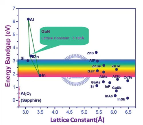
Figure. 1.1 The bandgap diagram of compound semiconductor materials.
Figure. 3.1.1. The schematic of experimental Photoluminescence setup.
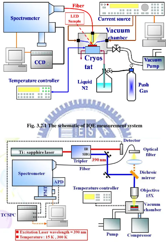
Figure. 3.2.1. The schematic of IQE measurement system.
Figure. 3.3.1. The schematic of EL measurement system.
Figure. 3.4.1. The picture of electroluminescence system
Figure. 4.2.1. The schematic drawing of sample structure.
Figure. 4.2.2. The schematic drawing of fabrication processes of LED.
Figure. 4.3.1. Top view CL images at corresponding emission peak wavelength.
Figure. 4.4.1.1 Schematic band diagrams of localized state due to In fluctuation.
Figure. 4.4.1.2 FWHM of three samples at different carrier density.
Figure. 4.4.2.1 Emission energy at different power density.
Figure. 4.5.1. Temperature dependent PL intensity range from 10 to 300 K.
Figure. 4.6.1. IQE as a function of excitation power at 15K and 300 K.
Figure. 4.7.1. Emission power as a function of current density of three sample.
Figure. 4.7.2. Emission efficiency as a function of current density of three sample.
Figure. 5.2.1. The schematic drawing of sample structure.
Figure. 5.3.1. Simulated hole distribution in reference and GQW LEDs.
Figure. 4.1 Current-dependent electroluminescence spectra .
Figure. 5.4.2. Current-dependent asymmetry factor of electroluminescence spectra .
Figure. 5.4.3. Current dependent emission energy and FWHM.
Figure. 5.5.1. Comparison of electroluminescence efficiency and L-I curves.
Chapter 1 Introduction
1-1 Wide bandgap III-N materials
Wide bandgap nitride materials have attracted great attention over the past
decades. The bandgap of the III-nitrides like AlN, GaN and InN material cover a very
wide range from 0.9 to 6.1 eV which represents the emission wavelength from deep
ultraviolet (UV) to infrared (IR) region as shown in Figure 1.1. This wide emission
wavelength range makes it promising for applying in the applications of
optoelectronic devices such as flat panel display, competing storage technologies,
automobiles, general lighting and biotechnology, and so on [1-4]. It is worth noting
that as the rapid developing of the blue region material research, we are able to fill up
the visible light gap and make the full color display by semiconductor material
becomes possible. Besides, the emitted short wavelength light in the blue and UV
region is especially suitable to pump up the yellow light and comes out a white light
output by mixing the original blue source and excited yellow light which realized the
solid state lighting. The III-nitride semiconductor material enjoyed some unique
properties that not only suitable for lighting source in short wavelength in visible
region but also high-speed/high-power electron device [5]. For example, it has high
considered as a next generation high efficiency lighting devices, III -nitride
semiconductors have some inherent drawbacks to deteriorate the lighting efficiency
like internal piezoelectric field and spontaneous polarization at heterointerface leading
to the quantum confined Stark effect (QCSE) and causing charge separation between
electrons and holes in quantum wells [8-9]. Even though, it is still worth to devote
more effort to overcome such problems for its great potential for realization of next
generation solid state lighting.
1-2 GaN-based LEDs
Basically, the blue GaN-based LED confronts some severe problems lowering the
efficiency and hindering the realization of solid state lighting. Lack of suitable
substrate GaN epitaxy is the most important issue. Nowadays, GaN material was
grown on sapphire susbtrate, which has a 15% smaller lattice constant than GaN, and
different thermal expansion coefficient. That leads to a very high defect density and
cracking of the layers when the structures are cooled down after growth. The problem
was firstly solved by Amano and Akasaki by designing and growing a AlN buffer
layer in 1986 [10]. Also, Nakamura grew GaAlN buffer layers on top of sapphire in
1991 [11] which make it possible to grow GaN on sapphire. In addition to the
problems by his two-flow growth reactor which opens the door of high quality GaN
material on sapphire [12]. The third problem of for GaN-based LED is p-type doping.
Every semiconductor lighting device needs p-n junctions. Previous to Akasaki’s work
p-type doping of GaN was impossibly. Akasaki (1988 at Nagoya University) found
that samples after Low Energy Electron Beam Irradiation treatment (LEEBI) showed
p-type conductivity [13-14]. Thus Akasaki demonstrated that in principle p-type
doping of GaN compounds was possible. Nakamura was then found the solution to
the puzzle of p-type doping. He found that previous investigators had annealed the
samples in Ammonia (NH3) atmosphere at high temperatures.Ammonia dissociates
above 400 oC, producing atomic hydrogen. Atomic hydrogen passivates acceptors, so
that p-type characteristics are not observed. Nakamura solved this problem by
annealing the samples in Nitrogen gas, instead of Ammonia [15]. Benefit by the effort
of such pioneers, the blue GaN-based light emitting diode (LED) is now successfully
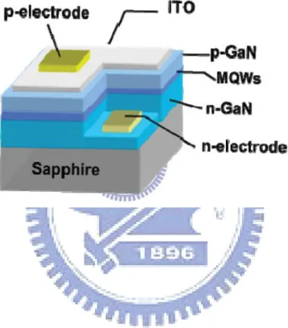
commercialized. The typical structure of a blue GaN-based LED is illustrated in
Figure 1.2. The layer of n -type GaN contains an excess of electrons,
whereas the p-type layer is a region from which electrons have been removed (i.e., in
which “holes” have been formed). If a forward bias is applied, electrons and holes can
recombine, releasing energy in the transition layer in the form of light. The energy of
Sapphire and silicon carbide are often used as substrates, which allow for large-area
heteroepitaxial growth.
1-3 Motivation
Typical InGaN/GaN LED are characterized by a substantial decrease in
efficiency as injection current increases. This phenomenon which known as efficiency
droop is a severe limitation for high power devices that operate at high current
densities and must be overcome to enable the LEDs needed for solid-state general
illumination. The efficiency droop is caused by a nonradiative carrier loss mechanism,
which is small at low currents but becomes significant for high injection currents.
Competition between radiative recombination and this droop-causing mechanism
results in the reduction in efficiency as current increases. The physical origin of
efficiency droop remains controversial, and several different mechanisms have been
suggested as explanations, including carrier leakage from the active region [16].
Auger recombination [17], junction heating [18], and carrier delocalization from
In-rich low-defect-density regions at high carrier densities [19]. Carrier leakage in
GaInN LEDs generally refers to the escape of electrons from the active region to the
p-type region. These leakage electrons may then recombine with holes either in the
therefore, fewer holes than electrons are injected into the active region. These two
phenomena that escape of electrons form the active region and reduced hole
concentration of any carrier leakage explanation for droop. Hole injected into the
active region may be the limiting factor, possibly due to the low p-type doping
efficiency or the electron blocking layer (EBL) acting as a potential barrier also for
holes. As a result of the low hole injection, current across the device is dominated by
electrons. Devices with p-type active regions which should increase hole injection
efficiency have been proposed as a solution to this problem.
However, it is not clear which cause the efficiency droops at high current. For
this study, we investigated the excitation power dependence PL intensity at room
temperature and temperature dependent intensity to confirm the confinement of
carrier in different structure. Then we discussed the normalized efficiency as a
function of injection current density at room temperature clearly and used APSYS
simulation to make sure our model is correct, so the physical mechanisms of current
dependent efficiency of InGaN/GaN LED has been confirmed.
This thesis is organized in the following way: In chapter 2, we give some
theoretical backgrounds and characteristics about InGaN/GaN MQW structures. The
experimental setups and theory are stated in chapter 3. In chapter 4, we present the
MQW LED with LT-GaN, InGaN/GaN and without prestrain layer. In chapter 5, we
show the experiment results and discuss for physical mechanisms of graded quantum
wells as a function of injection current density in InGaN/GaN LEDs. Finally, we gave
a brief summary of the study in chapter 6.
Chapter 2 Properties of Ⅲ-Nitride semiconductor
In this chapter, we show the properties of InGaN/GaN LEDs and prestrain
insertion layer in InGaN/GaN light emitting diodes. Efficiency droop behavior has
also be introduced
2-1 Quantum confinement effect in semiconductor nanostructure
The semiconductor nanostructure is widely used as the active layer in optoelectric devices such as light emitting diodes and laser diodes. This low dimension structure has the advantage of high emission efficiency because of the quantum confinement effect. Due to the different dimension of confinement, we can divide the nanostructures into several groups. For instance, the quantum well structure is confined in one dimension (1D), the quantum wire structure is confined in two dimensions (2D), and the quantum dot structure is confined in three dimensions (3D). In this thesis, we would discuss the quantum well structure in detail. When we discuss the quantum well structure, the excitons are confined in two dimensions. If the well width is much larger than aB in bulk, the exciton would not
feel any difference compared to the environment in bulk. However, if the well width decreases to the order of aB in bulk or even smaller than aB in bulk, the electrons and
holes would be strongly confined in the well and also increase the exciton binding energy.
With above discussion, the Hamiltonian of the relative motion can be written as
H=He ( xe, ye, ze ) + Hh ( xh, yh , zh ) + He-h ( r) Eq. (2.1.1)
where He and Hh are represented as the electron and hole motion confined in the well,
and He-h is the Hamiltonian described the Coulomb potential attracting the electron
different spatial confinement and r is the relative position vector between the electrons and holes. Therefore, the resolution of the Hamiltonian is given by
En= E en+ E hn - E e-h Eq. (2.1.2)
where E en and E hn is the energy of nth quantum confined state, and E e-h is the binding
energy of exciton. Then, the lowest exciton resonance energy associated with the ground states in the well can be described as
Eres = Eg + E en+ E hn - E e-h Eq. (2.1.3)
In actual situation, the exciton resonance energy is sensitive to the well width. When we use narrow well width, the confinement is improved. However, when the well
width is extremely narrow, there may be some leakage of the electron and hole wave function leading to the decreasing of the exciton binding energy. The emission
spectrum of the quantum well structure is affected by the competition between the quantum confinement energy level and that of exciton binding energy.
2-2 The electric field and localization effect in quantum well structure
In consequence of the polar crystal structure group III-nitride heterointerfaces are
charged [20, 21]. Strong electric fields therefore influence valence and conduction
band profiles at interfaces [21] and in quantum wells [22–25]. Any deformation of the
gallium nitride lattice modifies the interatomic distances as well as the polarisation of
the unit cell and occur in correlation with changes of interface charges and of the band
gallium nitride layers preceding the growth of the actual device structure is of high
interest. The built-in electric field in conventional c-plane heterstructures would result
in decreasing the oscillation strength of the separation of electron-hole pairs. Also, the
carrier recombination rate and the internal quantum efficiency would be
reduced.
However, in spite of the high density of dislocations and large separation of
electron-hole pairs, the InGaN-based heterostructures grown on c-plane sapphire still
have the high luminescence efficiency. It is reported that the luminescence efficiency
enhancement is due to the effective localization of excitons in the In-rich regions [29].
The mechanism of this unique behavior in InGaN-based heterostructures is still
unclear. Several groups suggested that the localization of excitons might induce by the
composition fluctuation and the phase separation [30,31]. In the In-rich regions, it
would provide a deep potential minimum within the InGaN layers, which would
confine electrons and holes tightly. Once the carriers injected into the InGaN-based
heterostructures, they will not be captured by the defects or dislocations. The
effectively trapping of carriers improved the radiative recombination rate.
Otherwise, the exciton localization is influenced by quantum well thickness, In
content, and doping level. The increase of In content may increase the effective
2-3 The basic concept of inserting prestrain layer
In general, the light output for a multiple quantum well (MQW) light-emitting
diode (LED) depends on the internal quantum efficiency (IQE) and the light
extraction efficiency (LEE). The former case mainly depends on the quality of
materials and their heterointerfaces within the active region. In addition, the quality of
the layer interfaces below and above the active region would also affect LED
performance. For GaN-based LEDs, the influence of magnesium or silicon dopants in
InGaN/GaN MQW on the IQE of GaN-based LEDs has been reported in previous
studies. Their performances could be also improved by the insertion of a prestrain
layer(s) between the InGaN/GaN MQW and the n-GaN [33].It has been proposed that the high luminescence efficiency results from successfully reducing compress strain and enhancing quality in active regions. However, the In fluctuation in the InGaN l a y e r s m a y a l s o i n d u c e m o r e n o n r a d i a t i v e d e f e c t d e n s i t i e s a n d influence efficiency at high carrier density.
2-4 The basic concept of efficiency droop
Solid-state lightings, especially InGaN/GaN light-emitting diodes (LEDs), have
been vigorously developed to take the place of traditional lighting source, due to its
which necessitates high efficiency at high current densities. However, as the
efficiency of LEDs increasing, the upcoming challenge is the efficiency “droop” for
high-power applications [34]. The external quantum efficiency EQE reaches its peak
at current densities as low as 50 Acm2 and monotonically decreases with further
increase in current.[35] It means that the efficiency reduces rapidly when LED
operating under high carrier density. Contrary to what may appear at an instant glance,
dislocations have been shown to reduce the overall efficiency but not affect the
efficiency droop. The major cause of efficiency droop is still a huge controversy.
Various possible mechanisms of droop including carrier overflow [35], non-uniform
distribution of holes [36, 37], Auger scattering [38], carrier delocalization [39],
junction heating have been proposed, but the genesis of the efficiency droop is still
the topic of an active debate. Although Auger recombination was proposed for the
efficiency droop,[40]the Auger losses in such a wide bandgap semiconductor are
expected to be very small,[41] which has also been verified using fully microscopic
many body models.[42] In addition, if an inherent process such as Auger
recombination were solely responsible for the efficiency degradation, this would have
undoubtedly prevented laser action, which requires high injection levels, in InGaN
which is not the case. The efficiency droop was also noted to be related to thequantum
increasing well thickness.[43] It was suggested that the effect of polarization field
may be playing a role.[44] The observations, however, are consistent with large
effective mass of holes because of which it is very likely that only the first QW next
to the p-barrier substantially contributes to radiative recombination. Making the well
wider, therefore, increases the emission intensity providing that the layer quality can
be maintained. Ithas also been suggested that in wider QWs the carrier density is
reduced for the same injection level and thus reduced Auger recombination.[44] What
is very revealing is that in below barrier photoexcitation experiments (photons
absorbed only in the QWs), where carriers are excited and recombined in the QWs
only, the efficiency droop was not observed at carrier generation rates comparable to
electrical injection which indicates that efficiency droop is related to the carrier
Chapter 3 Experimental instrument and setup
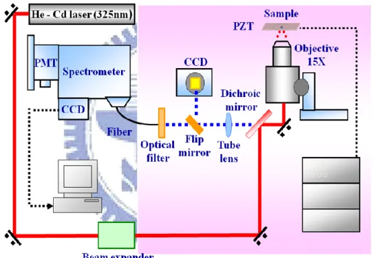
3-1 Photoluminescence (PL)
PL spectroscopy has been used as a measurement method to detect the optical
properties of the materials because of its nondestructive characteristics. PL is the
emission of light from a material under optical excitation. The laser light source used
to excite carriers should have larger energy band gap than the semiconductors. When
the laser light is absorbed within the semiconductors, it would excite the carriers from
the valence band to the conduction band. Then, it produces the electrons in the
conduction band and the holes in the valence band. When the electron in an excited
state return to the initial state, it will emit a photon whose energy is equal to the
energy difference between the excited state and the initial state, therefore, we can
observed the emission peak from PL spectrum.
The photoluminescence spectroscopy is the optical measurement to examine the
quality and optical characteristic of material.First, when we analysis a new compound
semiconductor, we can use PL measurement to know the band gap of the new
material. Second, the intensity of PL signal is contributed to the amount of radiative
the material quality and the recombination mechanisms of the materials.
The carrier recombination processes occur in many ways in order to reach the
equilibrium. Those processes can be divided into radiative recombination and
nonradiative recombination. We can recognize the radiative recombination easily at
low temperature by PL measurement, since it would not be influenced by the thermal
energy.
If there are some defect energy level existed in energy band gap of
semiconductor, they could also contribute to radiative recombination process.
Therefore, we could observe the multiple emission peaks in the PL spectrum, and the
intensity of the emission peaks is related to the contribution of the individual radiative
recombination process.
The schematic setup of our PL system is shown in Fig. 3.1.1. The pumping source
was a multi-mode and non-polarized Helium-Cadmium laser operated on 325 nm
with 35 mW. After reflecting by three mirrors, the laser light was focused by a lens
which focal length was 5 cm, to 0.1 mm in diameter and the luminescence signal was
collected by some lens. The probed light was dispersed by 0.32 monochromator
(Jobin-Yvon Triax-320) with 1800, 1200, and 300 grooves/mm grating and the
maximum width if the entrance slit was 1 mm. In order to prevent the laser coupling
temperature-dependent PL measurement, all the samples were placed in the
closed-cycle cryostat with a temperature controller ranging from 20 K to 300 K.
3-2 IQE measurement system
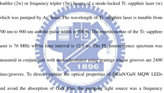
The schematic setup of our IQE measurement system is shown in Fig. 3.2.1.The
pulsed excitation source for the IQE measurement is provided by the frequency
doubler (2w) or frequency tripler (3w) beams of a mode-locked Ti: sapphire laser (w)
which was pumped by Ar+ laser. The wavelength of Ti: sapphire laser is tunable from
700 nm to 900 nm and the pulse width is 200 fs. The repetition rate of the Ti: sapphire
laser is 76 MHz whose time interval is 12.5 ns. The PL luminescence spectrum was
measured in conjunction with monochromator using gratings whose grooves are 2400
lines/grooves. To direct examine the optical properties of InGaN/GaN MQW LEDs
and avoid the absorption of GaN film, the pumping light source was a frequency
doubled Ti: sapphire laser operated on 390 nm. And all the samples were placed in the
closed-cycle cryostat with a temperature controller ranging from 20 K to room
temperature.
3-3 Electroluminescence (EL)
Fig. 3.3.1 shows the schematic of low electroluminescence measurement systems.
the patterned electrode of sample surface, three axial stages for probe and fiber to
detected the light output, and a cryostat for the cooling system which use the liquid
helium to cooling the chamber. Then, the light detected by a 0.32 m monochromator
(Jobin-Yvon Triax-320) with 1800, 1200, and 300 grooves/mm grating and the
maximum width if the entrance slit was 1 mm.
Fig. 3.2.1 The schematic of IQE measurement system
Fig. 3.3.1 The schematic of EL measurement system
Chapter 4 Optical and electrical properties of InGaN/GaN multiple
quantum wells with and without prestrain layer
4-1 Introduction
Generally speaking, lattice constants in the lateral plane of the substrate and
quantum well are different and there exist strains in one or both of components. The
strains change the energy gaps, the curvature of the valence bands, and consequently,
the effective masses of the holes. Therefore, the quantum confined valence subbands
are modified by the biaxial strains. The biaxial strains also lead to the piezoelectric
field along the Z direction in wurtzite materials. It inclines the one-dimensional
confinement potential. The quantum confinement energy levels and the corresponding
envelop function in such potential are different from those in the original confinement
potential. This is easily understood that imaging the field pushes the electrons and the
holes toward the opposite walls in the well because of opposite charges. Thus the
overlap of the electron and hole wave function is reduced and this reduction is
expected to result in the decrease of the exciton binding energy. Therefore, optical
properties under the presence of the piezoelectric field are expected to be considerably
4-2 Sample structure and Fabrication
The sample in this study are commercial InGaN/GaN MQW LEDs and grown
by metalorganic chemical vapor deposition (MOCVD). The sample in this study
grown on c-plane (0001) sapphire substrates. The sample structure consist 2μ m
undoped n-GaN, a 2μ m Si-doped n-type GaN, and an unintentionally doped active
layer with InxGa1-xN/GaN MQWs, and a 20nm p-AlGaN electron blocking layer
(EBL), and 120nm Mg-doped p-type GaN(Cladding layer). The doped concentration
of n- and p-type GaN is nominally 5 × 10¹⁸ and 1 × 1019 cm-3, respectively, the
MQWs layer comprise 6 periods InGaN well (~2.5 nm) and GaN barrier (~12 nm),in
composition is 15%. In this study, LED samples with the InGaN/GaN insertion layer
were labeled as LED-I, which comprise 10 periods InGaN layer(~1nm) and GaN
layer(~5nm),in composition is 6%. Sample with a low temperature growth GaN
prestrain layer was labeled as LED- II. The LT-GaN prestrain layer grown at 840。C,
this growth condition has higher vertical-to-lateral growth rate ratio compared to a
high growthtemperature. This may allow LT-GaN layer to release strain from lattice
mismatch. While LEDs without the insertion layer were also prepared for
comparison and labeled as LED-III. The sample structure is shown in Fig. 4.2.1. The
fabrication processes of InGaN/GaN LED show in Fig. 4.2.2 . In this study, we insert
by the lattice mismatch between sapphire and GaN, In this study, an LT-GaN prestrain
layer was used and compared with general InGaN/GaN prestrain layer. The difference
between sample I and sample II may affect the internal quantum efficiency and the
efficiency droop at high carrier density, hence, we will study the relation between
localized state in quantum well and physical mechanisms of quantum efficiency.
4-3 CL image measurement and discussion
For this study, the spatially resolved CL images were obtained by scanning the
scanning emission microscopy over the samples.The observed submicron-scaled CL
inhomogeneities should be due to the spatial fluctuation of the energy band gap,
which is mainly created by the spatial distribution of indium composition in InGaN
active layers.Fig.4.3-1(a),(b),and(c) shows the top view CL images of LED with
LED-I, LED-II, and LED-III. It can be seen clearly that emission pattern of (b) and (c)
were both inhomogeneous. In contrast, Sample with LT-GaN prestrain layers has the
most uniform emission image at corresponding peak emission wavelength. The
various emission area observed from sample with prestrain layers and without
prestrain layers indicate that elastic relaxation occurred in the prestrain layers by
surface undulations. Since the indium segregation to form emission pattern
strained In–N bonds, indium atoms can preferentially segregate to the ridges from the
troughs of the undulated surface. As a result, In-rich regions will be formed near the
surface. Therefore, the density of In-rich regions in InGaN/GaN prestrain layers was
larger than that in LT-GaN prestrain layers. This will result in the formation of In-rich
regions due to these In-rich surface.
4-4 Power dependent PL measurement
4-4.1 Carrier localization effect
Due to composition inhomogeneity and monolayer thickness fluctuation Of
InGaN QWs self-organized In-rich region is generated in InGaN active region,
resulting in potential fluctuation of energy bandgap. AS shown in Fig.4.4.1.1 As
injected carrier density increases further, an occupation of high energy stats of
localized centers will be enhanced. And the band filling effect will make the carriers
more easily escape from localized states to extendend states which decrease IQE.
From the Fig 4.4.1.2 we could found that LED without prestrain layer structure has
much higher FWHM under the same carrier density. At carrier density above
1x10¹⁸(#/cm3), the FWHM increase fast and the band filling effect is start to dominate.
From Fig 4.4.2, we can see sample III has larger FWHM than others, which means In
On the other hand, the LT-GaN and InGaN/GaN prestrain sample has similar band
width at low carrier density. However, as carrier density above 1x10¹⁸ (#/cm3), the
sample with LT-GaN prestarin layer has smaller band width than InGaN/GaN
prestrain layer which means smaller band filling effect. The possible reason of
reducing In fluctuaction of LT-GaN prestrain layer sample may relating to using
GaN film can more effectively eliminate In incorporation in active regions than InGaN film.
4-4.2 Reduction of pizeoelectric field
Several research groups have reported that the internal electric field existed in
InGaN/GaN QW structure. This internal electric field through the QW tilts the
potential band and leads to a spatial separation of electrons and holes in the QW,
resulting a decreasing in degreed of wave function overlap which is called the QCSE.
The internal electric filed in the QW can be screened by photogenerated carriers.
Consequently, the QCSE effect become weaker when the carrier density increased,
resulting in the emission peak wavelength buleshift and IQE enhanced at low injected
carriers region. . Figure 4.4.2.1 shows the emission peak energy under different input
power. When the input power was increase, the peak energy of the emission spectra of
input power before 10mW may be explained by the carrier screening of the QCSE
resulting from piezoelectric fields.[45][46] When the prestrain layer was inserted
between n-GaN and MQW, the bule shift by screen effect are decrease from 20meV
to only 10meV. We now analyze the spontaneous PL in the InGaN samples in more
detail. We explain the PL behavior differences of the LED with and without prestrain
layer by quantum confinement and the predominant strong piezoelectric field in thin
quantum wells. Indeed, in hexagonalnitride MQWs, the quantum-confined Stark
effect arises due to the piezoelectric field.[46] We analyzed the influence of
nonequilibrium carriers on the position of PL spectra in the InGaN/GaN MQWs using
a triangular well model. The photoexcited carriers screen the internal field. For an
idealized case, neglecting thermal distribution in the bands, the emitted quantum
energy hn for band-to-band recombination in a quantum well in the presence of
n o n e q u i l i b r i u m e l e c t r o n – h o l e p a i r d e n s i t y n c a n b e e x p r e s s e d a s ) ( ) ( ) ( ) ( ) (n edF n E n E n E n E
hv g e e h .Here, Eg(n) is the carrier density
dependent forbidden gap, which, taking into account band-gap renormalization, can
be expressed as 3 1 ) 0 ( ) (n E n
Eg g with β=2x10⁻⁸ eV cm; d is the well width; F(n) is the internal electricfield strength, which can be expressed as
0 ) 0 ( ) ( ned F n F
with maximum field strength F(0 )and static relative dielectric constant ε, which has
triangular well bottom for electrons and holes, respectively, and can be calculated from 13 23 , 2 , ] 8 ) ( 9 [ ) 2 ( F n m E h e h e
. The effective masses of electrons or holes, me,h ,
used in the calculations have been assumed to be 0.25m0 , mh>m0 , respectively[47].
In order to compare our experimental results with the calculations, we expressed hv as
a function of excitation power density P (in MW/cm2), which for the case of
predominantly square-law recombination are related as[48] n =n P hv , where
α is the absorption coefficient for laser light and has been taken as 1.5X105 cm-2, and γ
is the square-law recombination coefficient and has been taken as[49] 4.8x10⁻¹¹ cm3
s-1.
The results of these calculations for InGaN/GaN MQWs are also illustrated in
Figure 4.4.2.1 by the dotted line. This rather crude model gives remarkably good
agreement between experimental data and theoretical estimations for more than four
orders of excitation power density (up to 10 kW/cm2). Note that a number of other
effects were not included in our model (we neglected the two-dimensional nature of
the system, carrier distribution in the barriers and the wells, excitonic and
nonradiative recombination channels, possible recombination coefficient change due
to separation of the carriers in wells, etc.). The F0 of reference was found to be equal
to 1.21 V/cm, which is quite similar to other evaluations in similar semiconductor
the value of 0.68 and 0.73MV/cm, which is much smaller than sample III. From the
above experiment result and data analysis, we can conclude that the use of LT-GaN
prestrain layer release the biaxial strain in quantum well for a certainty.
4-5 Temperature dependent PL measurement
In order to further clarify the influence of the carrier confinement ability of
LED with and without prestrain layer, temperature dependent PL measurements were
performed. The Fig. 4.5.1 shows Arrhenius plots of the normalized integrated PL
intensity for the InGaN-related PL emission over the temperature range from 20K to
300K. It was found that the integrated PL intensity dropped slowly with temperature
during the low-temperature region, whereas it decreased rapidly during the
high-temperature region. The best fitting gives three activation energies of about 51,
45, and 32 meV for InGaN/GaN, LT-GAN, and without prestrain layer, respectively.
In general, the quenching of the luminescence with temperature can be explained by
thermal emission of the carriers out of a confining potential with an activation energy
correlated with the depth of the confining potential [49]. It has suggested that the
localization of carriers operates as excellent radiative recombination centers. In other
words, high localization energies of excitons will provide deep potential wells that
carrier localization in the active layer also has a significant effect on the performance
of LEDs, resulting in an increase in radiative recombination efficiencies[50].
4-6 The measurement of internal quantum efficiency
From the preview result, we know that LT-GaN prestrain did change the property
of active region. For this study, we used the IQE method which S. Watanabe et al.
proposed to determine the IQE of InGaN/GaN MQW LEDs to study the IQE of
different structure. The internal quantum efficiency can be calculated by
EX EX PL PL PL
E
I
E
I
C
/
/
(4.6.1)where IPL and IEX are PL intensity and excitation intensity, respectively. EPL and EEX
are PL photon energy and excitation photon energy, respectively. C is a constant
affected by mostly carrier injection efficiency by laser, light extraction and correction
efficiency of PL, and does not depend on either excitation power density or
measurement temperature. First, we measured the excitation power dependent PL
intensity at low and room temperature, and then the relative PL quantum efficiency
curves can be obtained by using equation 4.6.1. And the constant C would be canceled
out by normalizing the curves to the peak value at the lowest temperature, because it
efficiency curves will not depend on carrier injection efficiency by laser, light
extraction and correction efficiency of PL. Therefore, the PL efficiency would be find
out from this model.
In tradition, the IQE is estimated by assuming that IQE is 100 % at low
temperature regardless of excitation power density. However, IQE is strongly
dependent on injected carrier density. Consequently, it is more reasonable to assume
the peak of PL efficiency at lowest temperature is equal 100 %, and then the IQE
curves as a function of excitation power and temperature can be understand.
Moreover, to avoid the absorption of GaN, the frequency doubled femtosecond
pulse Ti: sapphire laser of 390 nm was used to excite sample, the excitation power
density was changed from 0.01 to 80 mW, and calculated injection carrier density is
ab out 2 .0 × 1 01 5 t o 1. 6 × 1 01 8 cm- 3 b y u s i n g t h e eq u at i o n b el ow : objective active InGaN GaN GaN active loss R d d f d h P density
carrier *exp( )*(1 exp( )) *
* * * ) ( ( 4 . 6 . 2 )
where P is excitation power, hν is energy of incident light, φ is laser spot size, f is
repetition rate of laser, dactive is the active layer thickness, αGaN is the absorption of
GaN, αInGaN is absorption of InGaN, R is reflection of sample surface, and Lossobjective
is transmission loss of objective.
carrier density at 15K and 300 K. We can observe that the IQE increases with
increasing injected carrier density to reach its maximum. As injected carrier density
further increases, then the IQE decreases. The tendency of two efficiency curves at 15
K and 300 K is very similar. But under low injected carrier density region, the IQE
curve at 300 K increases obviously than it at 15 K. The results indicated that the IQE
at 15 K saturated more easily than it at 300 K.
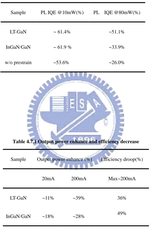
The experimental results indicated that the IQE are about 61.9 %, 41.4 % and
53.6% at injected carrier density is 4.7 × 10¹⁷ #/cm3(~20mA) for sample I, sample II
and sample III, respectively. Table 4.6.1 shows the value of IQE, We believe the
higher internal quantum efficiency for the LED is due to the better crystalline quality,
attributed to reducing of threading dislocations and releasing strain from sapphire ,so
enhance the carrier confinement ability as studied in previous work [51]. However,
when carrier density increase to 1.6 × 10¹⁸ #/cm3 ,the IQE are about 33.9 %,and 51.1
% for LED with InGaN/GaN and LT-GaN prestrain layer. Under similar quality and
strain release order, the LED with LT-GaN insertion layer has much higher efficiency
4-7Current dependent intensity and efficiency discussion
Fig.4.7.1 shows the light output power versus injection current (L–I)
characteristics of these LED samples. When a 20-mA current injection was applied to
the LEDs with emitting wavelength of 460 nm, the output powers enhancement of
LED-I and LED-II were approximately 11% and 18%, respectively. Even InGaN/GaN
LED has higher output power enhancement at 20mA, as injection current increase to
200mA, the LT-GaN LED has larger output power enhancement than InGaN/GaN
LEDs. In addition to the improvement of light output power for the LED. Note that
three samples, regardless of having InGaN/GaN, LT-GaN or without prestrain layer
between active region and n-type GaN show almost the same current density
dependency of forward voltage. As shown in Fig. 4.7.2, the EQE rapidly decreases as
the forward current increases up to 200mA, resulting in the serious EQE droop of ~
54%. However, the MQW LEDs with LT-GaN prestrain layer show very different
dependency of the EQE on the forward current density, EQE very slowly decreases
with increasing the forward current density, showing the magnitude of EQE droop of
approximately 36% at Jf of 200 mA. Table 4.7.1 shows the value of output power
enhancement and efficiency decrease. These results indicate that LT-GaN prestrain
layer facilitate the suppression of In inhomogeneous distribution in the active region ,
Figure. 4.3.1 Top view CL images of (a) LT-GaN prestrain layer, (b)InGan/GaN prestrain (c) w/o prestrain structure at corresponding emission peak
wavelength
Figure. 4.4.1.2 FWHM of three samples at different carrier density
Figure. 4.4.2.1 Emission energy of (a)LT-GaN (b)InGan/GaN (c)w/o prestrain structure at different power density.
Figure. 4.5.1 The Arrhenius plot of the integrated PL intensity obtained from the main emission peak over the temperature range from 10 to 300 K.
Figure. 4.7.1 Emission power as a function of current density of three sample
Table 4.6.1 IQE of InGaN/GaN, LT-GaN and without prestrain layers
InGaN/GaN LED at 10 and 80mW
Sample PL IQE @10mW(%) PL IQE @80mW(%)
LT-GaN InGaN/GaN w/o prestrain ~ 61.4% ~ 61.9 % ~53.6% ~51.1% ~33.9% ~26.0%
Table 4.7.1 Output power enhance and efficiency decrease
Sample Output power enhance (%) Efficiency droop(%)
20mA 200mA Max~200mA
LT-GaN ~11% ~39% 36%
49% InGaN/GaN ~18% ~28%
Chapter 5 Analysis of the reduce efficiency droop by Graded
quantum wells structure
5-1 Introduction
In recent years, great efforts have been made to reduce the efficiency droop.
Most of them are focus on minimizing the carrier overflow by reduce or eliminate the
polarization field in the active region, such as using polarization matched multiple
quantum wells (MQWs) [52, 53], staggered InGaN quantum wells [54], and non-polar
or semi-polar GaN substrate [55]. But for improving hole distribution, only several
approaches, such as p-type MQWs [56] or coupled quantum wells [57], are explored.
However, in the p-type MQWs, the Mg-dopant is very likely to diffuse into wells,
while in the coupled quantum wells, electrons are tend to overflow by using thin
barriers. These will result in reduction of radiative efficiency. In this research, we
designed and grew a new LED structure with graded-thickness multiple quantum
wells (GQWs) by using metal-organic chemical vapor deposition (MOCVD). Better
hole distribution in such graded-thickness designed MQWs were demonstrated by
APSYS simulation as well as the electroluminescence (EL) measurements.
5-2 Sample structure and fabrication
buffer layer, ten-pair InGaN/GaN superlattice were grown on the top of sapphire.
After that, six-pair MQWs were grown with 10-nm-thick GaN barriers. For our
designed experiment, the thicknesses of In0.15Ga0.85N quantum wells for GQW LED
structure, controlled by growth time, are 1.5, 1.8, 2.1, 2.4, 2.7, 3 nm along [0001]
direction. While the reference LED structure has a unique well-thickness of 2.25 nm.
It’s worth noting here that the total volumes of active region for the two samples are
the same. Finally, a 20-nm-thick electron blocking layer with Al0.15Ga0.85N and a
120-nm-thick p-GaN layer were grown to complete the epi-structure. The sample
structure is shown in Fig. 5.2.1. For EL measurements, the LED chips were fabricated
by regular chip process with ITO current spreading layer and Ni/Au contact metal,
and the size of mesa is 300×300 μm2
.
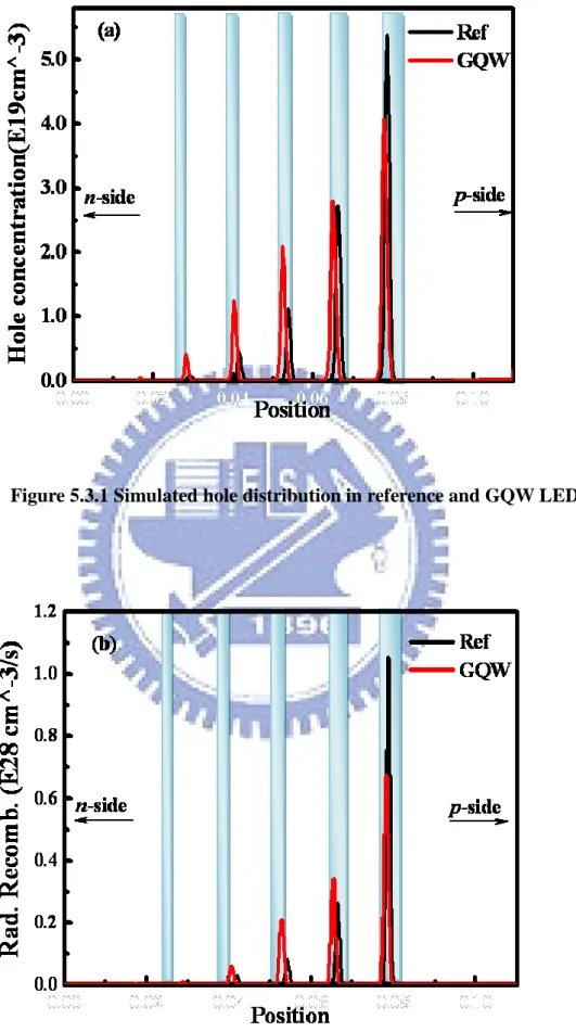
5-3 APSYS simulation of electron and hole concentration distribution
Based on our experimental structures, we built up the model of the reference and
GQW LED structures. The typical LED structure was composed of 2-μm-thick n-type
GaN layer (n-doping=2E18 cm-3), six pairs of In0.15Ga0.85N/GaN MQWs with
10-nm-thick GaN barriers, 20-nm-thick p-Al0.15Ga0.85N electron blocking layer
(p-doping=5E17 cm-3), and 120-nm-thick p-type GaN layer (p-doping=1E18 cm-3.
in Ref. [58]. Commonly accepted Shockley-Read-Hall recombination lifetime
parameters (several nano-seconds) are used in the simulations. Figure 5.3.1 and
Figure 5.3.2 shows the simulated hole distribution and radiative recombination
distribution along MQWs at 100 A/cm2. For reference LED structure, it can clearly be
seen that holes mostly concentrate in the QW nearest p-side (denoted as the first QW),
so does the radiative recombination. This phenomenon coincides with the optical
measurement result in ref. [59], which is mainly due to poor transportation of holes.
While in the case of GQW LED structure, the hole concentration decreases in the first
QW by about 16%, but increases in the second, third, and fourth QWs by 7%, 94%,
and 175%, respectively, as compared with reference LED. It indicates that the holes
are more capable of transporting across the first QW, consisted with our hypothesis.
On the other hand, electrons are relatively not being affected due to their high
mobility. Therefore, more wells will participate in the recombination process, as
illustrated by the radiative recombination distribution in Fig.5.3.2 Moreover, due to
the relative low carrier densities in the first QW and more uniform of carrier
distribution, the possibility of Auger scattering and carrier overflow can be lower.
5-4 Current dependent electroluminescence measurement and analysis
The electroluminescence EL spectra of the LEDs were easured using a pulsed
current source with 1% duty cycle and 2us pulse width, to eliminate the heating effect.
Light was collected by an optical fiber placed above the diode and connected to a
computer controlled sepectromemter equipped with a charge coupled device detector.
Different well width has different emission energy, so the GQW LED has larger
band with than reference LED at whole current range. And which has been mentioned
before is LED with thicker QW will emission longer wavelength due to QCSE effect.
So, The emission energy is of GQW LED is smaller than reference LED at small
current density, as the injection increase, the peak energy will increase with injection
current due to band filling effect, and the GQW LED has larger emission energy at
high current density . Under the same current density, LED with thicker well width
should has smaller peak energy (small band filling effect), however, in our
experiment , the GQW LED has invert result, which means carrier might transfer
from the widest well width QW to thinner well width QW close to n-type GaN.
Therefore we can conclude that graded quantum does has better carrier transport
ability.
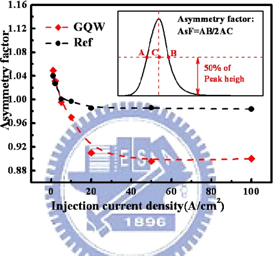
According to the simulated results mentioned above, more holes distribute in the
narrower well, the intensity of shorter-wavelength part in emission spectrum will rise.
Thus, the symmetry of spectrum might be changed, as can be seen from the power
dependent of EL spectrum in Fig. 5.4.1. To investing EL spectrum in detail, the
asymmetry factor (AsF) was calculated. As illustrated inset of Fig.5.4.3, it can be
defined as the distance from the center line of the peak to the back slope (AB) divided
by twice the distance from the center line of the peak to the front slope (2AC), with all
measurements made at 50% of the maximum peak height. The calculated AsF under
every injection level for both samples are summarized in Fig. 5.4.2. It can clearly be
seen that, AsF of reference LED decreases slightly from 1.04 to be about 0.98 when
injection current increases from 1 A/cm2 to 100 A/cm2. While GQW LED showes
larger variation, the AsF starts at 1.05 (0.1 A/cm2) and saturates at about 0.89 (after 20
A/cm2). According to the definition of AsF, if the bluer light emits from narrower
wells, the symmetry of spectrum would be interrupted and smaller than 1.
To further study the mechanisms responsible for the variation of the graded
quantum structure, more electrical properties were investigated as below. Fig.5.4.3
shows the emission peak energy (a) and FWHM (b) of spectra as a function of the
injected carrier density at room temperature for both LEDs of graded guantum well
and reference. In Fig.5.4.3several unique optical properties were observed. First, the
to screening effect and band filling effect. And we can see, at low injection current,
GQW LED has smaller emission peak energy and larger FWHM. The reason is when
LED is under low injection current, only the quantum well which closest to p-type
GaN generate light, and the GQW one has wider well width than reference. However,
at high current density, we can observe the emission energy of GQW is larger than
reference, it is due to carrier transport to thinner well which close to n-type GaN and
emission short wavelength of GQW LED. The rapidly increase in FWHM of GQW
also prove this penominace. Therefore, we can conclude that GQW does have
superior radiative recombination distribution, which leads to the EL spectrum
blueshifts and broadens significantly with increasing the injection current.
5-5 Analysis of injection carrier density dependence EL efficiency and efficiency droop
Finally, we investigated the efficiency droop behaviors in both LEDs. The output
powers of LEDs and the normalized efficiency (η) of refrence and GQW LED are
plotted in Fig. 5.5.1 as a function of injection current, which are obtained by
integrating the light intensity of EL spectrum measured by spectrometer. The
electroluminescence EL spectra of the LEDs were easured using a pulsed current
source with 1% duty cycle and 2us pulse width, to eliminate the heating effect.
computer controlled sepectromemter equipped with a charge couple d device
detector. It can clearly be seen that the light output power enhancement at current
density of 22 A/cm2 and 244 A/cm2 for GQW LED is 36% and 71%. This indicates
that even with wider wells (worse wave function overlap for electrons and holes) near
p-side, the overall efficiency for GQW LED is still higher than reference, and the
utilization rate of MQWs is improved. More importantly, LED without any structure,
the relative efficiency reaches its high as 33.3 A/cm2 and efficiency shows only a
slight decrease 17% at 244 Acm2, as shown in Fig 5.5.1. The quantum efficiency
peaks at a higher current density and shows a lesser decrease as current density
increase. This improvement could be mainly attributed to the superior hole
distribution and radiative recombination distribution, and also the reduction of Auger
scattering resulting from the lower carrier concentration in QW nearest p-side. As the
main contribution to the optical emission is from the first QW next to the p-type
region. In fact, Li et al reported a shift of EQE peak position from 5 A/cm2 to over
200 A/cm2, but with a trade-off for the IQE, by widening QWs from 0.6 to 1.5 nm.
This observation, not the interpretation, is actually consistent with the report by
Gardner et al. in which case EQE reached its peak above 200 A/cm2 when the MQW
active layer was replaced by a double heterostructure with a 13 nm InGaN layer. This
reducing the carrier density in the wells. Furthermore, for the samples with graded
quantum well. It should be noted that despite the pulsed measurements and pushing of
the efficiency peak to higher currents, the droop is still affected by heating since a red
shift not shown of the EL peak position beyond 300 A/cm2 is observed.
Figure 5.3.1 Simulated hole distribution in reference and GQW LEDs
Figure5.4.1 Current-dependent electroluminescence spectra of (a) GQW and (b) reference LEDs.
Figure 5.4.2. Current-dependent asymmetry factor of electroluminescence
Figure 5.4.3 Current dependent emission energy and FWHM in reference and GQW LEDs
Figure5.5.1. Comparison of normalized electroluminescence efficiency and L-I
Chapter 6 Conclusion
In first part, we have compared LEDs with LT-GaN, InGa/GaN and without
prestrain layer. The LED with LT-GaN prestrain layer shows a great improvement in
outpower and efficiency from the LED with InGa/GaN prestrain layer at high carrier
density. The use of LT-GaN results in a very little blue shift of emission, less band
filling effect, and reduce efficiency droop at high carrier density, compared to the
reference and InGaN/GaN prestrain LEDs. These results indicate that low temperature
growth GaN prestrain layer facilitate the suppression of the strain and In
inhomogeneous distribution. Further, we have demonstrated relatively low efficiency
droop in InGaN/GaN LEDs by graded quantum well structure as compared with the
normal LEDs. The EQE is nearly retained in GQW LEDs even at a high forward
current density of 244 A/cm2(only 17 % droop), whereas c-plane LEDs exhibit as
high as 36% efficiency droop under the same injection current density. The light
output power was also enhanced by 36% at 22 A/cm2 due to more quantum well be
used. The APSYS simulations indicate that superior hole distribution can be achieved
in the GQW designed MQWs, in which the well-thickness increases along [0001]
direction. It might be attributed to the longer radiative recombination lifetime in the
wider well nearest to p-type layer. Moreover, by analyzing the EL spectra in detail, the
more carriers distribute in the following wells, which agrees well with the simulated
results. As a result, the efficiency droop behavior was alleviated from 54% in LED
without any structure modified to 17% in LED with LT-GaN prestrain layer and
graded quantum well. In addition, This work implies that with suitable active region
design, carrier transportation behavior could be modified, which is very useful for
Reference
[1] S. Nakamura, M. Senoh, N. Isawa, and S. Nagahama, Japan Journal of Applied
Physics 34,L797 (1995)
[2] S. Nakamura, T. Mukai, and M. Senoh, Applied Physics Letter 64, 1687 (1994)
[3] S. Nakamura, M. Senoh, S. Nagahama, N. Iwasa, T. Yamada, T. Matsushita, Y.
Sugimoto, and H. Kiyoju, Applied Physics Letter 70, 868 (1997)
[4] S. Nakamura, Science 281, 956 (1998)
[5] Y.Arakawa, IEEE Journal of Selected Topics in Quantum Electronics 8, 823
(2002)
[6] H. Morkoc, Nitride Semiconductors and Devices (Springer Verlag, Heidelberg),
1999
[7] S. N. Mohammad, and H. Morkoc, Progress in Quantum Electronics 20, 361,
(1996)
[8] F. Bernardini and V. Fiorentini, Physica Status Solidi B 216, 391 (1999)
[9] A. Hangleiter, J. S. Im, H. Kollmer, S. Heppel, J. Off, and F. Scholz, MRS
Internet Journal of Nitride Semiconductor Research 3, 15 (1998)
[10] H. Amano, N. Sawaki, I. Akasaki, and Y. Toyoda, Applied Physics Letter 48,
353(1986)