國 立 交 通 大 學
電 控 工 程 研 究 所
碩 士 論 文
具雙調變機制且寬負載範圍之高效率高頻切換
直流-直流降壓式電源轉換器
Dual Modulation Technique for High Efficiency in High-switching
Buck Converters Over a Wide Load Range
研 究 生:黃 琮 瑛
指導教授:陳 科 宏 博士
具雙調變機制且寬負載範圍之高效率高頻切換
直流-直流降壓式電源轉換器
Dual Modulation Technique for High Efficiency in High-switching
Buck Converters Over a Wide Load Range
研 究 生:黃琮瑛 Student:Tsung-Ying Huang
指導教授:陳科宏 Advisor:Ke-Horng Chen
國 立 交 通 大 學
電控工程研究所
碩 士 論 文
A Thesis
Submitted to Department of Electrical Control Engineering College of Electrical Engineering
National Chiao Tung University in partial Fulfillment of the Requirements
for the Degree of Master in
Electrical and Control Engineering October 2010
Hsinchu, Taiwan, Republic of China
具雙調變機制且寬負載範圍之高效率高頻切換
直流-直流降壓式電源轉換器
學生:黃琮瑛
指導教授:陳科宏 博士
國立交通大學電控工程研究所 碩士班
摘 要
在現今可攜式電子產品的應用上,高效能和小型的電壓轉換器在提供
系統電源上扮演非常重要的角色。為了減少輸出級濾波器的面積,提出高
頻切換的直流轉直流降壓轉換器來達到元件整合的功能。
然而,對傳統的電流控制模式之直流轉直流降壓式電源轉換器來說並
不適合在高切換頻率下操作,因為系統的電源轉換效率在輕載時會急遽下
降以及控制器電路中所使用到的運算放大器會限制電源轉換器整體系統
的頻寬。換言之,轉換器在輕載時系統轉換效率的降低不適合商業上的應
用與電路頻寬的限制造成在高切換頻率下的不正確操作。為了解決以上提
到的問題,雙調變機制在本論文中被提出。
由於雙調變機制的使用,主調節器中的交流漣波偵測器不僅讓電壓轉
換器在高切換頻率下能夠正常操作而且能加速系統的暫態響應,而由次調
節器製造的跳頻切換脈波能做到減少功率開關元件的切換次數以達到提
高系統在輕載時的轉換效率。
本論文中,實現一個雙調變控制機制用來改善電源轉換效率伴隨著輸
出電壓漣波小幅的提高;所提出的交流漣波偵測器可以減輕輸出電容上的
寄生電阻與寄生電感在高速切換下所產生的切換雜訊。此外,雙調變機制
能夠在系統暫態響應時做到加快系統反應時間;且當系統操作在極輕載
時,系統操作頻率能維持在一高於音頻之最小值,避免系統產生噪音。實
驗結果顯示電源轉換器使用
1μH 的電感操作在 5MHz 的切換頻率,輸出
電壓為
1.8 伏特。負載電流在 150 毫安培與 450 毫安培間瞬間變換時的反
應時間小於
3μS;且電源轉換效率在寬負載範圍下可以維持在百分之八十
五以上。相較於傳統控制方式,輕載時的轉換效率最高可以改善百分之四
十五。
Dual Modulation Technique for High Efficiency in High-switching
Buck Converters Over a Wide Load Range
Student:Tsung-Ying
Huang
Advisor:Dr. Ke-Horng Chen
Institute of Electrical Control Engineering
National Chiao Tung University
ABSTRACT
For today’s portable electronic device applications, high performance and compact size voltage regulator plays an important role to provide system power. To reduce the size of output filter, a high switching dc-dc buck converter is presented to achieve high integration.
However, the conventional current mode DC-DC buck converter is not suitable for high switching operation, because the system conversion efficiency deceases drastically at light load condition and the operational amplifiers of control circuits restrict system’s bandwidth. That is to say, the drop of the efficiency at light load makes the converter not suitable for commercial application and the limitation of circuit bandwidth causes incorrect operation at a high switching frequency. To solve these issues mentioned above, the dual modulation technique is presented in this thesis.
Owing the dual modulation technique, the AC ripple detector in primary modulator not only makes converter operate at a high switching frequency correctly but also speeds up the transient response, and the hopping switching pulse produced by secondary modulator reduces switching times of power switches to raise efficiency at the light load condition.
In this thesis, a dual modulation technique to improve power conversion efficiency with minimal increase in output voltage ripple is presented. The worsening switching noise caused by parasitic resistance and inductance due to high-switching operation can also be alleviated by the proposed AC ripple detector. Furthermore, the dual modulation method can speed up the load transient response since the switching frequency can increase to 10 MHz during the transient period. At very light loads, the switching frequency is always kept higher than the acoustic frequency to avoid noisy sound. Experiment results show that the converter operates at 5MHz using a small inductor of 1μH. The load transient response time is shorter than 3μs when load current changes from 150 to 450mA or vice versa. Power efficiency is kept higher than 85% over a wide load current range. Specifically, light efficiency can be raised to about 45% above that of the conventional design.
誌 謝
即將完成碩士的研究生涯,心中無限感慨,在此要感謝的是指導教授
─陳科宏老師;無論其於行為品格,及其研究熱忱、執著與嚴謹的態度,
給予我無條件悉心指導與啟發,帶領我進入類比電路設計的領域;也感謝
老師給予實驗室優良完善的訓練環境以及豐富的研究資源。
感謝國林學長帶領我進入電源管理晶片的領域,在我剛進實驗室時花
了許多時間指導我,替我打下足夠的基礎面對日後的研究,是我研究所的
啟蒙老師。
感謝夥伴仁杰學長、王為,一起參與計畫、撰寫 Paper,是我研究所
生活中不可多得的好夥伴。感謝同儕逸群、士偉、典融、智宇、銘彥,在
研究生活中相互切磋、同甘共苦。
感謝昱輝學長、契霖學長、俊禹學長、銘信學長、耀沂學長與已畢業
的學長、姊們,給予研究上的諮詢與照顧以及學弟、妹們平時的協助。
最後,要感謝我的父親、母親給我精神與物質上的支持鼓勵使我能全
力專注於碩士學位的攻讀。以及女友惠鈞,一直以來陪伴在我身邊尤其在
兩年的研究所生活與我分享當中的苦與樂。
黃琮瑛
國立交通大學
2010.10.15
Contents
Chapter 1 ... 1
Introduction ... 1
1.1 Background of Power Management System ... 1
1.2 Classifications of Voltage Regulators ... 3
1.2.1 Linear Regulator ... 3
1.2.2 Switched Capacitor Circuit ... 4
1.2.3 Switching Regulator ... 6
1.2.4 Comparison ... 8
1.3 Motivation ... 8
1.4 Thesis Organization ... 10
Chapter 2 ... 12
Basic Knowledge of Switching Regulators ... 12
2.1 Topologies of DC-DC Converters ... 12
2.2 Technologies of Controlling Modulator ... 14
2.2.1 Pulse Width Modulation (PWM) ... 15
2.2.2 Pulse Frequency Modulation (PFM) ... 17
2.2.3 Hysteretic Control Technique ... 18
2.3 Specifications of Switching Regulators ... 20
2.3.1 Power Conversion Efficiency ... 20
2.3.2 Load and Line Regulation ... 22
2.3.3 Transient Response ... 22
Chapter 3 ... 25
The Theory of the Dual Modulation Technique in High Switching Buck Converters ... 25
3.1 High Switching Operation Issues ... 25
3.2 Design Concept Description ... 26
3.2.1 Dual Modulation Technique ... 26
3.2.2 AC Ripple Detection Technique ... 29
3.2.3 Summary ... 31
3.3 Loop Analysis ... 32
Chapter 4 ... 38
Circuit Implementation ... 38
4.1 Hopping Frequency Modulator (HFM) Circuit ... 39
4.2 Frequency Hopper ... 40
4.3 Loading Potential Detector (LPD) Circuit... 42
4.4 Voltage Adder ... 43
Experimental Results and Conclusion ... 46
5.1 Experimental Results ... 46
5.1.1 Performance of Steady State ... 48
5.1.2 Performance of Transient Response ... 50
5.1.3 System Efficiency Comparison ... 51
5.2 Conclusion ... 53
5.3 Future Work ... 53
Figure Captions
Fig. 1. The block diagram of cell phone system. ... 2
Fig. 2. The energy constrained operation. ... 2
Fig. 3. The basic structure of linear regulator. ... 4
Fig. 4. The conventional structure of voltage doubler. ... 6
Fig. 5. The structure of buck type voltage mode control switching converter. ... 7
Fig. 6. The Conventional Current Mode Buck Converter. ... 10
Fig. 7. The three topologies of DC-DC converters ... 13
Fig. 8. Waveforms of pulse width modulation. ... 16
Fig. 9. Combination of conduction loss and switching loss in PWM control. ... 16
Fig. 10. Control signal waveforms of pulse frequency modulation. ... 17
Fig. 11. Combination of conduction loss and switching loss in PFM control. ... 18
Fig. 12. The structure of hysteretic control technique. ... 20
Fig. 13. The transient response of output voltage relates to load current. ... 24
Fig. 14. Waveforms of the buck converter with the dual modulation technique. ... 27
Fig. 15. Efficiency and hopping frequency versus load current for the proposed converter system. ... 28
Fig. 16. The proposed buck converter with the dual modulation technique. ... 29
Fig. 17. The concept of current sensing flow as it utilizes the AC ripple detector. .. 31
Fig. 18. Small-signal model of the AC ripple control buck converter. ... 32
Fig. 19. Bode plot of the proposed converter system. ... 37
Fig. 20. The schematic of HFM circuit. ... 40
Fig. 21. The schematic of frequency hopper. ... 41
Fig. 22. The schematic of loading potential detector. ... 43
Fig. 23. The schematic of voltage adder. ... 44
Fig. 24. The schematic of AC ripple detector. ... 45
Fig. 25. The chip micrograph. ... 46
Fig. 26. Waveforms of the output voltage and inductor current at different load current conditions. (a) ILoad =5 mA. (b) ILoad =20 mA. (c) ILoad =110 mA (d) ILoad =220 mA. ... 49
Fig. 27. Load transient response. (a) Load current steps from 150mA to 450mA or vice versa. (b) Load current steps from 1mA to 500mA or vice versa. The modulation rapidly switches between the secondary and the primary modulation techniques. ... 51
Fig. 28. (a) Efficiency comparison between the original PWM operation and the proposed dual modulation technique. (b) Efficiency of the proposed converter over a wide range of load current. ... 52
Table Captions
Table I. Comparative table of power management circuits. ... 8
Table II Comparative table of power management circuits. ... 11
Table III. Comparisons of three converter topologies. ... 14
Table IV. Comparisons between PWM and PFM controls. ... 21
Table V: Design parameters of the proposed converter. ... 36
Chapter 1
Introduction
Nowadays, portable devices are popularly used such as cell phones, digital cameras and MP3 players, etc. The more functions in one product, the more competitive in marketing. However, the multi-function in portable devices makes the demand on supply energy increase greatly. That is to say, extending the battery life has become an important issue determined by the power management module. Thus, minimizing power loss and effective energy usage on power management ICs are two major topics to achieve the enhancement on power conversion efficiency. In this chapter, we will show the background and basic knowledge of power management system in chapter 1.1 firstly. The classification of power management circuits which including switching converters, linear regulators, and charge pump converters will show in chapter 1.2. The motivation will give in chapter 1.3. Finally, the thesis organization will show in chapter 1.4.
1.1 Background of Power Management System
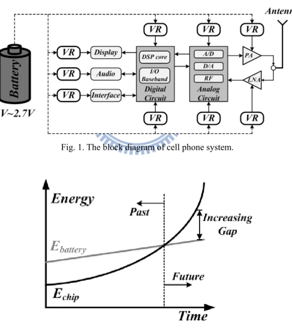
For portable power applications, the multi-level supply constructed by voltage regulators is an important technology. For example, the block diagram of cell phone system is shown in Fig. 1 [1]. Voltage regulator circuits (VR) regulate the battery voltage to provide different level voltage to suitable blocks: audio, display, interface, DSP core, analog circuits, and digital circuits. The system will operate in different modes, such as sleeping mode, communication mode and so on. The control unit is needed to control the internal power management block enable or disable, respectively. That is to say, by using control unit can enhance system efficiency of power supply circuits, such as linear regulators, switching regulators and charge pumps. When this technology is used, the energy consumption can be
reduced compared to that with the battery supply only [2].
As shown in Fig. 2, due to the increasing functionality and complexity in every single chip, the requirement on energy raises rapidly, make the growing of battery energy is not enough to supplying power of chips in the future. An easy method to solve is enlarging the capacity of batteries, but the increasing volume of portable devices isn’t pleased to see because of user’s convenience. In order to minimize the cost, the ability of saving power and increasing of power conversion efficiency is an important issue, that’s why the power management system playing an irreplaceable role in analog integrated circuit design.
Fig. 1. The block diagram of cell phone system.
1.2 Classifications of Voltage Regulators
General power management circuits used in portable devices can be classified into three technologies: linear regulators, switched capacitor circuits, and switching regulators. These voltage regulators will be introduced in briefly in this section, and comparisons will be given finally, including load ability, efficiency, circuit complexity, efficiency and so on.
1.2.1 Linear Regulator
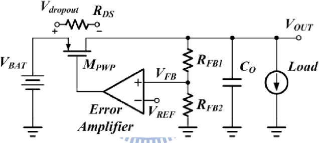
The basic structure of linear regulator is shown in Fig. 3 [3], it’s also called low drop-out (LDO) voltage regulator because of a drop out voltage (Vdropout) between input and
output voltages about 100~500mV. An error amplifier controls the gate voltage of the pass transistor (MPWP) with respect to a reference voltage (VREF). These devices are constructed
in a feedback configuration to maintain the output voltage irrespective of the load current variations. The power transistor has equivalent resistor (RDS) from input to output, so the
size of power transistor should be well designed to fit the regulated output voltage and load ability.
The advantages of linear regulator are described as follows. One is the circuit structure is simple, make the die size is the smallest in all kind of voltage regulators, another is linear regulator only uses feedback resistors and error amplifier’s output analogy signal to control power transistor, it makes a purely analogy operation environment without any digital base circuits. So there is no Electro Magnetic Interference (EMI) issue and no output ripple.
There are two major disadvantages described as follows. Firstly, because of without dual storage components, the linear regulators only can do buck regulation. Secondly, since the output current must pass through the series transistor which consumes the dropout voltage between the output and input voltages, the efficiency is low for large voltage across
input and output voltages. The efficiency that depends on the difference of input and output voltages is given by (1).
OUT LOAD OUT OUT LOAD IN OUT LOAD IN
V
I
V
V
I
V
V
I
V
(1)The major applications that use linear regulators can be classified to digital and analog. The digital applications include Digital Signal Processors (DSP), Input/Output (I/O) modules and memory type devices. Analog applications include signal-path applications such as power amplifier (PA) and Phase lock loop (PLL).
Fig. 3. The basic structure of linear regulator.
1.2.2 Switched Capacitor Circuit
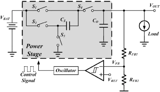
The switched capacitor circuit is also called chare pump, is used to generate a dc voltage higher or lower than the supply voltage or opposite in polarity to the supply voltage in low power applications. Charge pumps use capacitors as energy storage devices. The capacitors are switched to deliver energies to obtain desired output voltage. Fig. 4 illustrates a conventional switched capacitor voltage doubler [4].
The switches S1 and S3 are closed during the first interval of the switching period,
period, the switches S2 and S4 are turned on and the voltage across capacitor CS is placed in
series with the input to generate an output voltage that is twice the input voltage. In order to maintain the output voltage, there are many ways to modulate the output voltage of a switched capacitor circuit to a desired value. The most straightforward method is to use a control circuit and an error amplifier. The error amplifier senses the output voltage variations via the feedback resistors. The control circuit fed from the error amplifier controls switches S1~S4 to regulate output voltage to a stable value through a voltage
control oscillator.
Depending on the hysteric feedback control and reference voltage, both buck and boost type can be used in switched capacitor circuits, and the circuit complexity is between linear regulators and switching regulators. But there is major drawback which is the load ability is depend on the size of output capacity (CO) and switching frequency. That is to say, larger
capacitor makes stronger load ability but consumes more chip size.
The charge pumps are useful in many different applications including low-voltage circuits, dynamic random access memory circuits, Electrically Erasable Programmable Read-Only Memory (EEPROM), and transceivers.
Fig. 4. The conventional structure of voltage doubler.
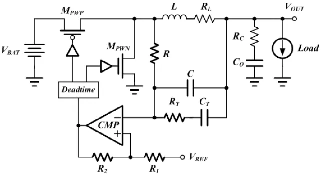
1.2.3 Switching Regulator
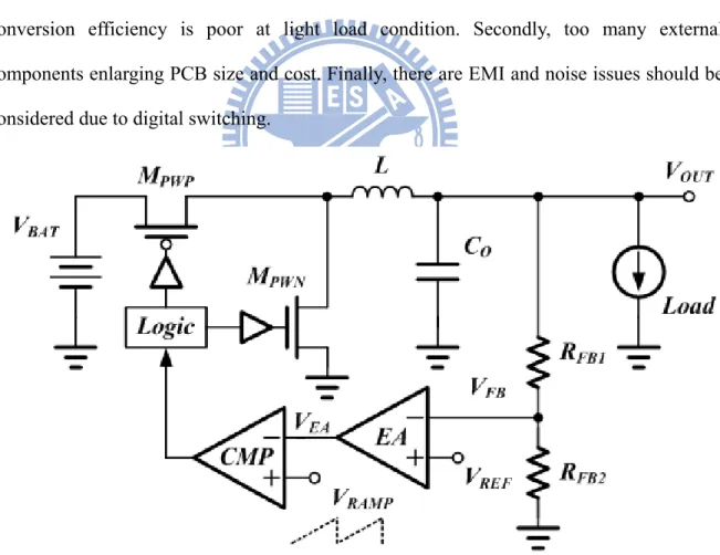
Switching regulators are widely used in power management system, because it has high efficiency and power handing capability. The conventional structure of buck type voltage mode control switching regulator is shown in Fig. 5 [5]. The regulator consists of a couple of complementary power transistors (MPWP MPWN), passive storage inductor (L),
output capacitor (CO), feedback resistors (RFB1 RFB2), and control circuits.
The circuit operation is described as follows. The error amplifier receives the output voltage variation and produces the error signal (VEA). The inputs of comparator receive the
error signal from error amplifier and the ramp signal (VRAMP) from ramp generator, then
compares the quantity between VEA and VRAMP to decide the duty cycle. After generating the
control signal, the logic block produce the detail timing to avoid short through current. Finally, control signals are sent to gate drivers to drive huge complementary power transistors. At the first subinterval, power PMOS (MPWP) turns on and power NMOS (MPWN)
turns off then supply source charges the inductor and the output capacitor. At the second subinterval, power NMOS (MPWN) turns on and power PMOS (MPWP) turns off then the
inductor will discharge to the output capacitor and load. As mentioned above, the switching regulator adjusts the output voltage error and regulates to correct voltage.
The advantages of switching regulators are described as follows. Firstly, the load ability is very large which in the range from no load to several amps. Secondly, the power conversion efficiency is high in medium to heavy load condition, up to 90%. Thirdly, switching regulators can operate in different kinds of type including buck, boost, and buck-boost type.
Nevertheless, there are some drawbacks described as follows. Firstly, the power conversion efficiency is poor at light load condition. Secondly, too many external components enlarging PCB size and cost. Finally, there are EMI and noise issues should be considered due to digital switching.
1.2.4 Comparison
A comparison table of power management circuits is listed in Table I. From Table I, we can conclude that switching regulators are best choices for power supplies driven portable application because of their high efficiency and large power handling capability.
Table I. Comparative table of power management circuits.
Linear
Regulator
Charge
Pump
Sw
tching
Regulator
Regulation Type Buck Buck/Boost Buck/Boost/Buck-Boost
Efficiency Low Medium High
Power Capability Medium Medium High
Footprint Area Compact Moderate Large
Cost Low Medium High
Complexity Low Medium High
Noise Low Medium High
1.3 Motivation
Recently, switching power converters use a high-switching controller to reduce the size of the output filter for compact solution in portable devices, such as cellular phones, wireless devices, and Bluetooth applications. However, the design of a high-switching controller needs to consider carefully the power conversion efficiency and high-switching noise caused by parasitic components. In general, the efficiency of a converter is defined as the ratio of output power, Pout, to input power, Pin, as expressed in (2).
out out in out loss
P
P
P
P
P
(2)and Psw are the conduction and switching losses, respectively. Psys is the power loss in the
controller, which is composed of analog and digital circuits [6].
loss con sw sys
P
P
P
P
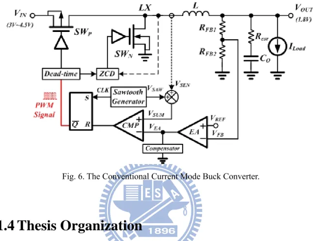
(3)The conventional pulse width modulation (PWM) of the current mode control (Fig. 6) becomes limited as switching frequency increases. The control system can have high efficiency at heavy loads as the Pcon is kept low by using low on-resistance of power
switches. Incidentally, efficiency decreases drastically when the load gradually decreases to no load condition since the increasing value of Psw dominates it. Specifically, the
high-switching operation resulting from the use of a small inductor could deteriorate efficiency. Thus, it is important to keep high efficiency over a wide load range.
The power converter system generally undergoes multiple operation modes in order to extend the battery life of present-day portable devices. Essentially, these include standby mode regulated by the pulse frequency modulation (PFM), burst mode to save on power, and normal PWM operation mode to sustain system operation [7]. However, the circuit complexity, output ripple, and noise issue are not effectively treated [8]. It deteriorates the performance of the power converter and limits the load current range.
Furthermore, in the current-mode control, high-switching frequency decreases system accuracy due to limited response time of the inductor current sensor [9]. In addition, the switching noise drastically increases to deteriorate the accuracy of current sensor to decrease the system stability.
Thus, it is important to improve the estimation accuracy of the inductor current for high-switching operation. In prior arts, the equivalent series resistance (ESR) on the output capacitor can be used to generate the current ripple to achieve fast load transient response through the two voltage feedback loops [10]. However, it suffers from large output voltage ripple [11]. In addition, using large ESR for system stability limits the selection of output
capacitor. Specifically, the large ripple reduces the performance of the sequent stage that needs small transient voltage dip.
Fig. 6. The Conventional Current Mode Buck Converter.
1.4 Thesis Organization
Therefore, the proposed dual modulation technique with the AC ripple detector needs to improve power conversion and remove high-switching noise to increase system stability simultaneously.
The dual modulation technique can separate the inductor current into the AC ripple signal and the loading potential signal. It can accurately acquire the inductor current information to decide the duty cycle without the need of large ESR. The loading potential signal not only can determine the optimum switching numbers for each power switch at different loads, it also can generate a hopping switching frequency at light loads for high-conversion efficiency. Furthermore, the hopping switching frequency should be higher than the acoustic frequency to avoid noisy sound. Compared with conventional PWM switching converters, the dual modulation technique can achieve faster transient response
and higher power conversion efficiency simultaneously with an acceptable output ripple. In addition, multilayer ceramic capacitors (MLCC) can be selected as the output capacitor for low cost.
Table II compares the converter with different control methods. The dual modulation mode not only has good efficiency but also reduces the output ripple and chip area compared with other methods. Specially, the audio noise, which is important issue for communication applications, can be effectively reduced.
The organization of this thesis is shown as follows. Chapter 2 introduces the design concept of the proposed dual modulation technique and the AC ripple detector. The close-loop analysis is described in chapter 3 to demonstrate the system stability. The circuit implementation is shown in chapter 4. In the chapter 5, experimental results can prove the correction of the dual modulation technique and the conclusion are demonstrated.
Table II Comparative table of power management circuits.
PFM
mode
Burst
mode
Dual modulation
mode
Efficiency Good Good Good
Circuit
Complexity Large Medium Small
Output Ripple Large Medium Small
Audio Noise Small Large Small
Chapter 2
Basic Knowledge of Switching
Regulators
In the chapter 2, the basic knowledge of switching regulators is presented. The three kinds of switching regulators including buck, boost, and buck-boost converters are introduced in section 2.1. The section 2.2 will show three kinds of controlling modulators including pulse width modulation (PWM), pulse frequency modulation (PFM), and hysteretic control technique in buck converters. Finally, the characteristics and performance specifications of buck converters are presented in section 2.3.
2.1 Topologies of DC-DC Converters
According to different placement of components, DC-DC converters can be classified into three types which are buck, boost, and buck-boost converters. These three types of converters are shown in Fig. 7 [12]-[14] and introduced in this section. All of converters consist of storage elements; power MOSFETs as the switch to control and drive large current by the control signal, and diode as another current passage to charge or discharge output loads. The control signal controls the energy from input to output by passing the power MOSFETs and regulated output to desired voltage.
The buck converter can only regulate a voltage lower than the input voltage. Contrarily, the boost converter only regulates a voltage higher than the input voltage. The buck-boost converter can regulate output voltage no matter higher or lower than the input voltage. A briefly comparison of three converter topologies characteristics are listed in the Table II. The conversion ratio is defined as dividing the input voltage into the output voltage, and
duty ratio (D) is defined as the power MOSFETs on time during one switching period.
(a) Buck type DC-DC converter
(b) Boost type DC-DC converter
(c) Buck-boost type DC-DC converter Fig. 7. The three topologies of DC-DC converters
Table III. Comparisons of three converter topologies. Buck Con erter Boost Converter Buck-boost Converter Conversion Ratio OUT IN V D V (CCM) 1 1 OUT IN V V D (CCM) 1 OUT IN V D V D (CCM) Conversion Type Step-down only Step-up only
D>0.5:Step-up D<0.5:Step-down
2.2 Technologies of Controlling Modulator
Although switching converters have high conversion efficiency, but the power loss will increase and result in efficiency reduction at different load conditions. The power consumptions can be classified with three parts. The first is the power losses due to large current pass through the equivalent resistance of the power MOSFET, the equivalent resistance can be expressed as RON, this power consumption is named conduction loss (PCON)
and expressed as follow.
2
CON OUT ON
P
I
R
(4)The second part is the charging and discharging alternately at large gate parasitic capacitor of the power MOSFET when the switching on and off periodically. This is a large loss of converters at light load condition named switching loss (PSW) and expressed as
follow.
2
(
)
SW GP GN IN SW
P
C
C
V
f
(5)The CGP and CGN are represented as gate parasitic capacitors of power PMOSFET and
frequency. The third is the quiescent current of converter’s internal controller to regulate output voltage at no load, it’s also called idle mode. This power consumption is named system power loss (PSYS) and defined the multiplication of quiescent current and input
voltage. That is to say, the power conversion efficiency of DC-DC converters can be defined the ratio of the output power and the total input power, and is expressed as follow.
100%
OUT OUT IN OUT LOSS
OUT
OUT SW CON SYS
P
P
Efficiency
P
P
P
P
P
P
P
P
(6)As above mentioned, the conduction loss (PCON) is dominated at heavy load because of
large output current flowing through the power MOSFETs. Contrarily, switching loss (PSW)
and system loss (PSYS) are dominated at light load condition because of slight output current.
So how to maintain high efficiency at wide load range is an important issue.
There are three most basic controlling methods named pulse width modulation (PWM), pulse frequency modulation (PFM), and hysteretic control technique. The following sections will introduce these controlling methods, respectively.
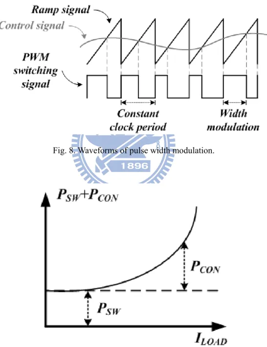
2.2.1 Pulse Width Modulation (PWM)
In PWM control operating, the power MOSFETs are controlled by a constant clock cycle, the PWM control waveforms are shown in Fig. 8 [15] [16]. While the ramp signal is lower than the control signal, the PWM signal at high level; contrarily, when the ramp signal is higher than the control signal, the PWM signal changes to low level. The main modulation is change the width of every clock cycle by the control signal and the output voltage is determined by the duty ratio of the PWM signal.
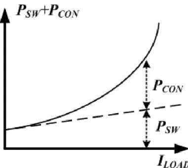
The conduction loss and switching loss are focused in PWM control operation. The summation of these two power loss is expressed as follows.
2
(
)
2CON SW OUT ON GP GN IN SW
P
P
I
R
C
C
V
f
(7)As shown in Eq. (5), the switching frequency is constant but output current varies with different loads. That is to say, the conduction loss maintains fixed but the switching loss is variable with loads. The summation of conduction loss and switching loss at different load can be shown in Fig. 9.
Fig. 8. Waveforms of pulse width modulation.
2.2.2 Pulse Frequency Modulation (PFM)
In PFM control operating, power MOSFETs are controlled by a vary frequency, the control waveforms are shown in Fig. 10 [17]. The on-time is fixed and off-time is variable determined by different loads in PFM control. By controlling the off-time of each switching cycle, the desired output voltage can be obtained. Therefore, the smaller output load could make switching frequency reduced.
The summation of conduction loss and switching loss in PFM control is the same with Eq. (5). In PFM control operating, vary switching frequency with different load conditions makes the switching loss reduced at light load, the diagram is shown in Fig. 11.
Fig. 11. Combination of conduction loss and switching loss in PFM control.
2.2.3 Hysteretic Control Technique
The hysteretic control structure is shown in Fig. 12 [18], the main control method is generating a hysteresis window. By controlling the upper and lower boundary to regulate the output voltage, when the feedback voltage touch to the hysteretic upper boundary, the power NMOSFET will turn on and PMOSFET will turn off to make the inductor current discharged and feedback voltage will decrease. At the same time, the hysteretic window will change to the lower boundary. While the feedback voltage touch to the hysteretic lower boundary, the power PMOSFET will turn on and the power NMOSFET will turn off to make the inductor current charged and feedback voltage will increase. The hysteretic window which is calculating by superposition theorem can be expressed as follows.
2 1 2 1 2 1 2 1 2 1 1 2
(
) (
)
H upper lower REF IN REF INV
V
V
R
R
R
V
V
V
R
R
R
R
R
R
R
V
R
R
(8)circuit is comparator, so there is no compensation issue without error amplifier. Secondly, without using any clock generator, the switching frequency of hysteretic controller is generated by system itself. The following is the calculation of feedback voltage variation, as expressed as follows. 0
0
(1
)
FBAVG FB OFF OFF FBAVG IN FBdV
V
V
I C
C
dt
R
t
t
V
DV
D T
V
RC
RC
(9)The voltage VFBAVG is the average voltage of feedback, ideally is DVIN, the parameter D,
is the duty ratio of the buck converter. Because the hysteresis window variation (VH) equals
to feedback voltage variation (△VFB). Combining the Eq. (8) and Eq. (9), the switching
frequency can as expressed as follows.
1 0 1 2 2 0 0 1
(1
)
1
1
(1
)(1
)
IN H FB INR
DV
D T
V
V
V
R
R
RC
R
f
D
D
T
RC
R
(10)By controlling the resistor R, capacitor C and the ratio of resistors R1 and R2 can define
the switching frequency, which is very suitable for high switching frequency design. Finally, because the output ripple has been defined, it can’t choose the low ESR capacitor to reduce output ripple.
Fig. 12. The structure of hysteretic control technique.
2.3 Specifications of Switching Regulators
Due to more and more electronics application need to be supplied by switching converter, the performances of switching converter have to be considered. The important specifications should be care about are listed as follows. Firstly, the power conversion efficiency of switching regulator is an important topic, how to maintain high efficiency over wide load range will be discussed in the section 2.3.1. The second is excellent load and line regulation, which will be discussed in the section 2.3.2. Final part is the transient response, how to immediately response when the suddenly large output current variation will be shown in the section 2.3.3.
2.3.1 Power Conversion Efficiency
The definition of switching regulator’s power conversion efficiency is the ratio of input power and output power and can be wrote as
OUT OUT OUT100%
IN IN INP
V
I
Efficiency
P
V
I
(11)The detail power losses and the operation range of control modulator have been shown in the section 2.2. Overall saying, the pulse width modulation (PWM) mode is suitable for operating in heavy load condition, and the pulse frequency modulation (PFM) is suitable for operating in light load condition. If the switching regulators operating only one module mode, take cell phone for example, the cell phone system operates in standby mode and many blocks of system doesn’t work, at light load condition but the converter only have PWM controller, as a result, the battery lifetime will reduce quickly. Hence, the best way to improve the efficiency is including the pulse frequency modulation (PFM) to control at light load condition. By dual mode control can keep high efficiency over wide load range. The comparison of PWM and PFM control technique will be listed in TABLE III.
Table IV. Comparisons between PWM and PFM controls.
Pulse Width Modulation Pulse Frequency Modulation
Well Efficiency Range Moderate to heavy load Light load
Frequency Constant Variable
Switching Loss of
Whole Load Constant
The heavier load the larger loss
Output Ripple Smaller Larger
Transient Response Faster Slower
Circuit Complexity Complicated Simple
2.3.2 Load and Line Regulation
Switching regulators are powerful system of stepping up or down the desired voltage. Therefore, to keep the regulated voltage and decrease the steady state error when varying the supply voltage and load condition of DC-DC converter is the most important.
The load regulation is defined as the percentage of steady state error of output voltage when the load condition changes and can be calculated as follows.
_
100
%
OUT
OUT desired load
V
Load Regulation
mA
V
I
(12)The line regulation is defined as the percentage of steady state error of output voltage when the input voltage changes and can be calculated as follows.
_100
%
.
OUT OUT desired INV
Line Regulation
mA
V
V
(13)2.3.3 Transient Response
The transient response is an important specification of DC-DC converter for the system applications. The large load current changes suddenly will cause a voltage fluctuation at output of DC-DC converter. The voltage fluctuation may trigger the logic circuit or affect the analog circuit. Therefore, it’s important to reduce the large voltage changing and the time during voltage variation. The transient response of output voltage relates to load current is shown in Fig. 13. During the first period Δt1, the large current flows into the
output load from DC-DC converter, due to the DC-DC converter cannot provide enough energy to maintain the output voltage, the output voltage will drop in this period because the output capacitor discharge the energy to support the load current. The drop voltage is shown in Eq. (14). According to the parameters of Eq. (11), selecting the output capacitor well can reduce the drop in this period.
1
1 2
drop drop OUT ESR O
t
V
V
I
R
C
(14)During the second period Δt2, the system senses the output variation by feedback loop
then turn on the power PMOSFET to recover the regulated output voltage. The summation of Δt1 and Δt2 is called the recovery time and the second period Δt2 depends on the system
bandwidth of the DC-DC converter
The static error ΔVOUT between light load and heavy load is relates to the voltage
regulator DC gain, the higher DC gain bringing the better load regulation [19]. Comparing to the Fig. 12(b) and Fig. 12(c), the performance of Fig. 12(b) due to the large DC gain and causes the better load regulation, but the second period Δt2 extends the recovery time.
However, it reduces the time of transient response. The performances of Fig. 12(c) due to the poor DC gain and cause huge static error but reduces the time of second period Δt2 and
improve the dynamic performance.
When the load current is decreasing to light load suddenly, the output voltage will jump until the DC-DC converter start to recovery the regulated voltage. The redundant current charges the output capacitor resulting to a peak voltage as shown in shown in Eq. (15) before the feedback loop of DC-DC converter reacts.
3
1 2
peak peak OUT ESR O
t
V
V
I
R
C
(15)During the final period Δt4 the output capacitor discharged the redundant current to
feedback resistors. As mention described, the transient response is relates to the bandwidth of DC-DC converter, output capacitor, equivalent series resistance (RESR) of output voltage
Chapter 3
The Theory of the Dual Modulation
Technique in High Switching Buck
Converters
In the chapter 3, we present the concept description of the proposed technique in high-switching converters. In the section 3.1, we discuss the drawbacks of the conventional switching converter operating at a high switching frequency. And the section 3.2 describes the analysis of the proposed dual modulation technique. Finally, the loop analysis of conventional V2 control and the proposed system are presented in section 3.3.
3.1 High Switching Operation Issues
The conventional switching power converters are suitable for normal operation frequency such as the range from 0.1MHz to 1MHz. The bandwidth and the operational phase delay of sub-circuits can be neglected because of the longer switching period. But lower switching frequency makes the output passive components including inductor and capacitor must be chosen larger values and need to be placed off-chip. That is to say, the cost increases due to the off-chip components and the larger PCB size.
In DC-DC buck converters, the inductor current ripple is inversely proportional to the switching frequency, so the size of output LC filter can be reduced due to the smaller inductor current ripple. Hence, in order to integrate the passive components into chip, increasing switching frequency is the most straightforward way.
When buck converter operates in high switching frequency, the internal controller of the converter may suffer from some problems. Firstly, the quiescent current of comparators
must be increased to have enough slew rate, it results more power consumption. Secondly, the inductor current signal is hard to be sensed due to the current sensing circuit doesn’t have enough bandwidth in conventional current mode control. Finally, the main power consumption is determined by the sum of the conduction loss and the switching loss. Arising switching frequency makes the switching loss increased, so the power conversion efficiency is deteriorated when load current decreases gradually. Thus, high switching converters are rare to be used in common commercial applications.
To solve the drawbacks mentioned above, the frequency hopping modulation technique with AC ripple detection is presented, and the design concept description of the proposed method is introduced in the next section.
3.2 Design Concept Description
3.2.1 Dual Modulation Technique
For high-switching operation, power conversion efficiency decreases drastically when load current changes from heavy to light. The dual modulation technique needs to hop switching frequency to find a trade-off between power conversion efficiency and output voltage ripple when load current decreases [20].
The timing diagram of the dual modulation technique is illustrated in Fig. 15. The original PWM control uses a high- switching signal VPRI to regulate the output voltage to
achieve a reduced ripple. Since the conduction loss dominates the whole power consumption at heavy loads, the high-switching signal would not result in a great decrease in efficiency. However, the switching loss drastically deteriorates efficiency from medium- to light-load condition due to the high-switching operation. Therefore, the secondary modulator becomes necessary to reduce the switching numbers as shown by the modulated signal VGATE used to control the power switches. At this time, dual modulation operates to
raise efficiency within an allowable output ripple.
Fig. 14. Waveforms of the buck converter with the dual modulation technique. The secondary modulator contributes to the decrease in the switching frequency and the increase in the hopping period. Light-load conditions require reduced switching frequency in order to save power. The hopping frequency modulator (HFM) circuit can determine a suitable switching frequency to reduce substantially the switching power loss at the power switches. Meanwhile, dual modulation starts to decrease the switching frequency from the constant fSW(constant) to fSW(dynamic) through the hopping frequency, fHOP, in the
secondary modulator. As depicted in Fig. 16, the value of fHOP varies with load current. In
addition, the hopping frequency not only reduces switching loss but also always keeps the output ripple within the allowable range.
The decrease in the switching frequency is accompanied with an increase in the hopping period as load current declines continuously. The decrease in switching frequency results in increased efficiency from a medium- to light-load condition. Much power is retrenched due to the switching loss reduction at the power MOSFETs. To further raise efficiency at very light loads, the primary modulator is shut down automatically and only the secondary modulator is employed to regulate the output voltage and to save much power in the quiescent operation loss. Furthermore, to avoid operation in the acoustic region, the hopping frequency is always kept higher than the acoustic frequency, facoustic, even at no
Fig. 15. Efficiency and hopping frequency versus load current for the proposed converter system.
3.2.2 AC Ripple Detection Technique
The architecture of the proposed dual modulation technique is shown in Fig. 16. The controller is separated into two parts. The primary modulator makes the system operate normally under high-switching frequency, and the secondary modulator can raise power conversion efficiency at light loads. Thus, high power conversion efficiency and a fast transient response under high-switching operations can be achieved.
Fig. 16. The proposed buck converter with the dual modulation technique.
The dual modulation technique should detect the load condition using the proposed loading potential detector (LPD) circuit. In addition, the combination of the LPD circuit and the error signal received by the error amplifier can be viewed as the control signal in the HFM circuit. As a result, the hopping signal generated by the secondary modulator can regulate the original PWM signal to find the trade-off between efficiency and output voltage ripple.
For high-switching converters, the conventional current sensing method may fail to provide accurate sensing load current due to limited bandwidth. Thus, it is better to find a
suitable current sensing method for the high-switching converter. Fig. 17 shows the concept of the proposed AC ripple control. In time domain, the output LC stage of the converter can be considered as a low-pass filter and work as an integrator.
However, the existence of ESR and ESL may deteriorate the accuracy of current sensing signal and the steady state duty cycle. Considering the ESR, Resr, and the equivalent series inductor (ESL), Lesl, on the output capacitor, CO, the output voltage ripple can be evaluated as the summation expressed in (16).
| | |
1
L
out out esr out esl out Co esr L esl L O
di
v
v
v
v
R i
L
i dt
dt
C
(16)Briefly, (16) is composed of overshoot voltage, vout|esr, across the ESR; induced voltage,
vout|esl, which is the differentiation of the inductor current with ESL; and voltage ripple,
vout|Co, which is the integration of the inductor current on the CO. Thus, it is convenient to
differentiate vout(t) in order to obtain the AC signal of the inductor current. This can be
expressed as 2 2 out L L L s esr esl O
dv
di
d i
i
v
R
L
dt
dt
dt
C
(17)At the right side of (17), the first and second terms represent the effect of the ESR and ESL, respectively. Owing to high-switching operation, the ESR and ESL seriously affect system stability and result in a large output ripple. The inductor current information can be accurately derived through the operation of the proposed AC ripple detector. The AC ripple detector behaves as a differentiator and inserts one low-frequency zero to increase system stability. One low-pass filter is utilized to filter out the high-frequency components contributed by the ESR and ESL. Consequently, the accurate inductor current can be derived as the PWM ramp since the effect of the ESR and ESL can be efficiently removed. In other words, the cheap MLCC can be selected as the output for low cost.
Fig. 17. The concept of current sensing flow as it utilizes the AC ripple detector.
3.2.3 Summary
To sum up the concept described above, the proposed dual modulation technique can solve the converter’s large switching loss in high switching frequency operating. Hence, the size of the output LC filter is reduced without consuming too much power consumption in the light load condition, it makes high switching converters are more suitable for common commercial applications. And the modified V2 control method can regulate output voltage even in zero-ESR condition, and the reduced output voltage ripple can make the converter more suitable for portable device applications. The V2 control topology contains two voltage feedback paths; the path from output voltage can rapidly react to the output voltage variation to speed up the transient response.
only can speed up the transient response, but also can maintain high power conversion efficiency over a wide load range.
3.3 Loop Analysis
Fig. 18. Small-signal model of the AC ripple control buck converter.
Fig. 18 shows the small-signal model of the dual modulation buck converter with the AC ripple detector [23]. The loop gain can be divided into two parts. The first part, which is the power stage, contributes duty-to-output transfer function and contains dual poles due to the output LC filter as expressed in (18) with a DC gain of Gvd0.
0 21
ˆ
ˆ
2
1
out esr vd vd O Os
v
G
s
G
d
s
s
1
1
1
where ,
,
and
2
O O esr O s esr O O LC
C
L
R
R C
LC
L
R
(18)The zero, ωesr, generated by Resr is pushed to high frequencies by using small ESR. RL
is the loading resistor and Rs is the series resistor of the LC resonant loop, which is the sum
of MOSFET on resistance, inductor resistance, and Resr.
The second part, composed of the controller, contributes the output-to-duty transfer function. In dual modulation, the control path contains two feedback loops, namely, the primary loop and the secondary feedback loops. The primary feedback loop is determined by the AC ripple detector and the error amplifier. Thus, the primary duty cycle can be decided through the signals, vs and vEA, by the PWM comparator. On the other hand, the
secondary feedback loop is determined by the error amplifier and the secondary modulator. The loop selection is determined by the LPD circuit. At very light loads, only the secondary modulator loop is selected as the feedback path. The feedback signal directly passes through the secondary modulator loop, ASEC(s), to generate the duty cycle. As load
current increases continuously, the feedback signal passes through both primary and secondary loops. Thus, dual modulation combines the primary and the secondary modulators at medium to light loads. At heavy loads, the feedback path is decided by the primary modulator when load current is larger than Iload(threshold). The feedback signal only
passes through the primary loop since the secondary loop ASEC(s) is disabled and the switch
is always connected to the primary path.
derived as (19).
_ _1
1
PI z PRI m o PI ps
A
s
G R
s
(19)The DC gain is constituted by the error amplifier’s transconductance, Gm, and the
output resistance, Ro. The PI compensator introduces one pole, ωPI_p composed of Ro and
compensation capacitor Cc, and one zero, ωPI_z composed of the compensation network, Rc
and Cc.
Similarly, the transfer function, ASEC(s) as shown in (20) contributed by the secondary
modulator, is used to provide a low-bandwidth response to filter out the high-switching PWM signal according to the load current. Thus, the DC gain of the ASEC(s) is inversely
proportional to the load current and controlled by Iload(threshold).
( ) 0 ( ) _ 1 _ 2 _ 1 _ 2 1 1 2 2 01
1
1
1
1
where , ,
and
is the low-frequency gain
load threshold load SEC SEC load threshold SEC p SEC p SEC p SEC p L L L L SEC
I
I
A
s
A
I
s
s
R C
R C
A
(20)The close-loop transfer function in the secondary modulator can be expressed as (21).
SEC vd PRI SEC
T
s
k G
s A
s A
s
(21)Therefore, the close-loop transfer function in dual modulation can be expressed as (22).
( ) ( )( )
loaddual PRI SEC load threshold
I
T
s
T
s
T
s
I
(22)As the load decreases continuously, the contribution of the primary modulation becomes smaller than that of the secondary modulation. At very light loads, the secondary
modulator can take over the control authority.
In this study, the primary modulation is demonstrated as follows: The control duty can be expressed as (23) to include the results from the AC ripple detector and the error amplifier.
1 2 1 2
ˆ
ˆ
ˆ
ˆ
where is the sensor gain
m PI m AC out
d d
d
F A
F B
k v
k
(23) Owing to the LC double poles, the AC ripple detector as a differentiator can introduce a low-frequency zero, ωAC, with a time constant, CdRd, to increase the system stability. Thus,
the transfer function, BAC(s), is shown in (24).
AC d d ACs
B
s
sC R
(24)In a steady state, the PWM comparator transfer functions Fm1 and Fm2 have the same
value of Fm as defined in (25).
1 2
m m m
F
F
F
(25)Thus, the output-to-duty transfer function can be derived as shown in (26). As expressed in (27), the system contains one single, low-frequency dominant pole, ωPI_p, and
two compensated zeros, ωzcomp1,2.
1 2 _1
1
ˆ
ˆ
1
zcom zcom m PRI AC m m o out PI ps
s
d
k F A
s
B
s
kF G R
v
s
(26) _ 1,2 21
4
where
and
1
1
2
m c d d PI p zcom o c d d m c cG R
C R
R C
C R
G C R
(27)As a result, the close-loop transfer function can be expressed in (28), which contains two zeros and three poles. According to design parameters shown in Table V, the position of the three poles and the two zeros can guarantee system stability during the primary PWM
operation.
1 2 0 2 _1
1
2
1
1
PRI m vd PRI AC zcom zcom m vd m o O O PI pT
s
kF G
s A
s
B
s
s
s
kF G G R
s
s
s
(28)Table V: Design parameters of the proposed converter. EA’s Gm 62.5 μA/V
Resistor Ro=90 MΩ Rc=150 kΩ Rd=5 MΩ
Capacitor Cc=30 pF Cd=2 pF
Three Poles f PI_p=59 Hz fO1=fO2=73 kHz
Two Zeros fzcom1=57.7 kHz fzcom1=91.5 kHz
Fig. 19 depicts the analytic Bode plot of the primary modulator with the AC ripple detector. Expectedly, the phase margin is larger than 45 degrees since the pole-zero cancellation of the proposed AC ripple detection technique is achieved without using a large ESR.
Chapter 4
Circuit Implementation
The architecture of the proposed buck converter has illustrated in Fig. 16. The converter is composed of a power stage, a feedback network, and the control stage including primary modulator and secondary modulator. The power stage contains a pair of power switches SWP and SWN, and an inductor L. Owing to high switching frequency, compact off
chip inductor and filtering capacitor CO can be used. Output voltage VOUT is scaled down to
VFB by the voltage divider, composed of resistors RFB1 and RFB2. The controller stage is
utilized to turn on/off power switches SWP and SWN.
In normal operation, the primary modulator produces the original PWM pulse to regulate output voltage. The comparator CMP compares the output signal VEA generated
from the error amplifier EA, with the summation of the sensing signal VS and the slope
compensation signal VSAW to decide system duty.
In light load condition, the secondary modulator generates the HFM pulse to combine with original PWM pulse. The LPD circuit generates VLoad, which stands for the load
condition, VLoad is combined with the error signal VEA to generate input control signal of
HFM circuit, VCtrl, and HFM circuit produces the optimal HFM pulse (VHOP) to modulate
with original PWM pulse (VPRI), the modulated control signal (VGATE) can reduce the
switching times of power switches to reduce the switching loss.
Furthermore, the primary modulator will shut down automatically in very light load or no load condition, and the secondary modulator can regulate the output voltage by itself to save much more efficiency.
The operation of the whole system is mentioned above. The operations of key sub-circuits in the control stage are explained in the following sections.