行政院國家科學委員會專題研究計畫 成果報告
超薄閘極氧化層 CMOS 元件軟崩潰效應研究(2/2)
計畫類別: 個別型計畫 計畫編號: NSC92-2215-E-009-024- 執行期間: 92 年 08 月 01 日至 93 年 07 月 31 日 執行單位: 國立交通大學電子工程學系 計畫主持人: 汪大暉 報告類型: 完整報告 報告附件: 出席國際會議研究心得報告及發表論文 處理方式: 本計畫可公開查詢中 華 民 國 93 年 10 月 28 日
行政院國家科學委員會補助專題研究計畫
■ 成 果 報 告
□期中進度報告
超薄閘極氧化層 CMOS 元件軟崩潰效應研究
計畫類別:■ 個別型計畫 □ 整合型計畫
計畫編號:NSC 92-2215-E-009-024-
執行期間:91 年 08 月 01 日至 93 年 07 月 31 日
計畫主持人:汪大暉
共同主持人:
計畫參與人員:蔡慶威、陳旻政、古紹泓、詹前泰、江欣凱、游建文
成果報告類型(依經費核定清單規定繳交):□精簡報告 ■完整報告
本成果報告包括以下應繳交之附件:
□赴國外出差或研習心得報告一份
□赴大陸地區出差或研習心得報告一份
■出席國際學術會議心得報告及發表之論文各一份
□國際合作研究計畫國外研究報告書一份
處理方式:除產學合作研究計畫、提升產業技術及人才培育研究計畫、
列管計畫及下列情形者外,得立即公開查詢
□涉及專利或其他智慧財產權,□一年□二年後可公開查詢
摘要
關鍵字:互補金氧半電晶體、絕緣層上覆矽、超薄閘極氧化層、可靠性、軟崩潰、 遲滯效應、flicker 雜訊(低頻雜訊)、浮動基極效應、漸進崩潰、漸進崩潰速率 當積體電路製程推進到奈米(sub-100nm)元件世代,絕緣層上覆矽技術的使 用將是可行性的替代方案之一。當元件尺寸縮小到 100 奈米時,閘極介電層的等 效氧化層厚度必須薄於 20 埃以下。然而,在如此薄氧化層的絕緣層上覆矽元件 中,軟式崩潰所引發之可靠性問題將是異常重要。 本研究報告將針對超薄氧化層絕緣層上覆矽金氧半場效電晶體中軟式 崩潰所引發之可靠性議題作一系列的探討。首先,在浮動基底極絕緣層上覆矽元 件中,吾人知道大量的基底漏電流所造成的基底電位的調變和所導致不可避免的 磁滯效應已被廣泛的討論。由於氧化層崩潰將增加基底極的穿隧漏電流,所以在 浮動基底極的超薄閘極氧化層絕緣層上覆矽元件中,崩潰位置對臨界電壓磁滯現 象的影響將在這部分探討。吾人將發表兩種在關閉狀態的金氧半電晶體中氧化層 崩潰增強磁滯現象的模型。吾人所提供的基底充電機制和實驗結果相符。在浮動 基底結構下的超薄閘極氧化層部份空乏絕緣層上覆矽金氧半場效電晶體中,軟式 崩潰增強的磁滯現象將成為一種嚴重的可靠性議題。 再者,吾人發現在浮動基底絕緣層上覆矽金氧半場效電晶體中通道軟式崩潰 導致一種新的低頻汲極電流雜訊退化現象。這種額外的雜訊來源來自於通道軟式 崩潰導致大量基底極的價帶電子穿隧電流產生微量的白雜訊放大所致。在超薄閘 極氧化層類比絕緣層上覆矽元件中,即使在操作電壓小於一伏特,通道軟式崩潰 增加額外的雜訊仍會發生並將成為一個重要的可靠性問題。 最後,直接穿隧效應也會對超薄氧化層的崩潰及元件之毀壞產生影響。一般來說,元件的毀壞與否是由氧化層崩潰所造成破壞程度所決定,代表破壞程度較 低的氧化層漏電流對實際電路應用而言,並不會造成任何操作上的影響。吾人在 p 型超薄氧化層絕緣層上覆矽電晶體中,針對浮動基底極對氧化層崩潰的破壞程 度作完整之研究。在 p 型超薄氧化層元件中,吾人發現了正偏壓基底極操作模式 下所產生的加速崩潰破壞。當氧化層初崩潰時,高能量的通道電洞在正偏基底極 時產生較大的電動加壓電流,進而使得氧化層產生更大的破壞。藉由熱載子光激 發實驗及熱電洞在通道能階上的分佈分析,吾人成功地解釋出此基底極偏壓相依 性。吾人並預測此種崩潰破壞將對浮動基底超薄閘極氧化層絕緣層上覆矽 p 型金 氧半場效電晶體產生新的可靠性議題。
Abstract
Keywords: CMOS, SOI, ultra-thin oxide, reliability, soft breakdown, hysteresis,
flicker noise (low frequency noise), floating body effect, progressive breakdown,
breakdown progression rate
The silicon-on-insulator (SOI) technology is a promising candidate of IC
manufacture required for sub-100nm CMOS devices. As device size shrinks below
100nm, the effective oxide thickness of gate dielectric must scale below 20Å. While, a great reliability concern induced by soft breakdown (SBD) in such thin oxides SOI
devices is being aroused.
The objective of this report is to investigate soft breakdown induced reliability
issues in such ultra-thin oxide SOI MOSFETs. First of all, substrate leakage current
has been known to cause substrate bias variation and induce unavoidable hysteresis
effects in floating body SOI devices. Since oxide breakdown can enhance substrate
tunneling leakage current, the impact of breakdown location on threshold voltage
hysteresis in ultra-thin oxide SOI devices is investigated in this part. Two breakdown
enhanced hysteresis modes in off-state CMOS are identified. The proposed body
hysteresis effect would be a serious reliability subject in ultra-thin oxide MOSFETs
with floating body configuration.
Moreover, a new low frequency drain current noise source in floating body
SOI nMOSFETs caused by channel soft breakdown is studied. The excess noise
originates from channel soft breakdown enhanced valence band electron tunneling
and the amplification by the small white noise of the substrate current. The c-SBD
enhanced excess noise may occur even with supply voltage less than 1.0V and would
be an important reliability problem in analog applications.
Finally, a large direct tunneling current can decrease oxide time-to-breakdown
and limit oxide further scaling. Actually in most circuits, the failure criterion is
determined by the hardness of oxide breakdown. In this part, floating body enhanced
breakdown progression in ultra-thin oxide SOI pMOS is proposed. The enhanced
progression is attributed to the increase of hole tunneling current resulting from
breakdown induced channel carrier heating. The substrate bias dependence of
post-breakdown hole tunneling current is confirmed through the calculation of
channel hole distribution in sub-bands. This observed phenomenon is significant to
Contents
中文摘要
iEnglish Abstract
iiiContents
vFigure Captions
viiTable Captions
xiChapter 1
Introduction
1Chapter 2
Soft Breakdown Enhanced Hysteresis Effects in
Ultra-Thin Oxide SOI MOSFETs
42.1 Introduction 4
2.2 Device Structure and Characterization 5
2.3 Modes of SBD Enhanced Hysteresis 7
2.4 Results and Discussion 8
2.5 Summary 9
Chapter 3
Soft Breakdown Enhanced Excess Low- Frequency
Noise in Ultra-Thin Oxide SOI n-MOSFETs
233.1 Introduction 23
3.2 Excess Low-Frequency Noise Model in SOI MOSFETs 24 3.3 Kink Effect Induced Excess Low-Frequency Noise 29 3.4 Channel Soft Breakdown Enhanced Excess Low-
Frequency Noise 31
Chapter 4
Floating Body Accelerated Oxide Breakdown
Progression in Ultra-Thin Oxide SOI p-MOSFETs
464.1 Introduction 46
4.2 Devices and Experiment 47
4.3 Result and Discussion 48
4.3.1 A Shorter tfail in SOI pMOSFETs 48
4.3.2 Mechanism of Enhanced BD Progression in SOI 48
4.3.3 BD Caused Carrier Heating 49
4.4 The Impact of Gate Stress Bias 52
4.5 Summary 52
Chapter 5
Conclusions
66References
68Publication List
81Figure Caption
Fig. 2.1 Gate current and substrate current versus gate bias in nMOSFETs. Solid line refers to an unstressed device and dashed line (dotted line) refers to a device after channel SBD (drain edge SBD).
Fig. 2.2 Body current versus drain bias in nMOSFETs. Solid line refers to an unstressed device and dashed line (dotted line) refers to a device after channel SBD (drain edge SBD).
Fig. 2.3 Gate current and substrate current versus gate bias in pMOSFETs. Solid line refers to an unstressed device and dashed line (dotted line) refers to a device after channel SBD (drain edge SBD).
Fig. 2.4 Illustration of two soft-breakdown enhanced floating-body charging processes in SOI nMOSFETs. (a) soft breakdown in the channel region and hole creation due to valence band electron tunneling; (b) soft breakdown in the drain region and enhanced GIDL current.
Fig. 2.5 Illustration of two soft-breakdown enhanced floating-body charging processes in SOI pMOSFETs. (a) soft breakdown in the channel region and valence band electron tunneling from poly-gate to the floating body; (b) soft breakdown in the drain region and enhanced GIDL current.
Fig. 2.6 Hysteresis in Ids and corresponding floating-body potential versus Vg in a
c-SBD SOI nMOSFETs. Measurement is performed with forward and then reverse drain sweeps from 0V to 1.3V.
Fig. 2.7 Hysteresis in sub-threshold current and corresponding floating-body potential in an e-SBD SOI nMOSFETs. Measurement is performed with forward and then reverse drain sweeps from 0V to 1.3V.
Fig. 2.8 The variation of body voltage Vb as a function of the amplitude of gate
Fig. 2.9 The variation of body voltage Vb as a function of the amplitude of drain
bias sweep in SOI nMOSFETs. Vg=0V.
Fig. 2.10 The variation of body voltage Vb as a function of the amplitude of gate
bias sweep in SOI pMOSFETs. Vd=0V.
Fig. 2.11 The variation of body voltage Vb as a function of the amplitude of drain
bias sweep in SOI pMOSFETs. Vg=0V.
Fig. 2.12 Illustration of dominant Vt hysteresis modes in the switching of an SOI
CMOS inverter.
Fig. 3.1 Noise sources in an SOI MOSFET.
Fig. 3.2 (a) Noise small-signal equivalent circuit for the floating-body and (b) schematic for the req and Ceq network.
Fig. 3.3 Typical input-referred low-frequency noise spectrum. Fig. 3.4 Low-frequency noise measurement setup.
Fig. 3.5 The Id-Vd characteristics in nMOS SOI devices with floating body and
grounded body when gate is biased at 0.9V.
Fig. 3.6 Normalized noise power spectral density in floating body nMOS SOI devices under different drain voltages with gate biased at 0.9V.
Fig. 3.7 Normalized noise power spectral density in grounded body nMOS SOI devices under different drain voltages with gate biased at 0.9V.
Fig. 3.8 Comparison of normalized noise power spectral density under different drain biases in floating body SOI devices and grounded body SOI devices at given frequency.
Fig. 3.9 The gate current and substrate current as a function of Vg in fresh, channel
SBD, and edge SBD n-MOSFETs are compared.
Fig. 3.10 The low frequency drain noise spectrums of a n-MOSFET before and after two SBD modes. The measurement drain bias is 0.1V and the gate bias is 1.2V.
Fig. 3.11 The normalized noise power spectrum of a c-SBD nMOS SOI device with floating body under different gate biases.
Fig. 3.12 Comparison of normalized noise power spectral density with floating body under different gate biases in a fresh device, c-SBD device and e-SBD device at f=100Hz.
Fig. 4.1 Comparsion of breakdown behavior in a 1.4nm oxide pMOSFETand in a 2.5nm oxide pMOSFET. The stress gate voltage is –3V for the 1.4nm oxide and –4.5V for the 2.5nm oxide. tBD denotes the onset time of oxide
breakdown.
Fig. 4.2 Oxide breakdown progression in bulk and SOI pMOSFETs. The stress gate bias is –2.9V and temperature is 125o C.
Fig. 4.3 The Weibull plots of tBD and tfail distribution for 1.6nm oxide SOI and bulk
pMOSFETs. The stress gate bias is –2.9V and the temperature is 125o C. tBD and tfail are defined as the time for gate current to reach 1.5 times and
15 times of its pre-stress value, respectively.
Fig. 4.4 The Vb dependence of pre-BD and post-BD electron currents (Ib) and hole
currents (Isd) at Vg=-1.5V. Distinct Vb dependence of the post-tBD Isd is
noted. The floating body configuration corresponds to a body voltage of approximately -0.65V. The inset illustrates carrier flow in a pMOSFET at a negative gate bias.
Fig. 4.5 The Vb dependence of the hole current Isd at different stress times, t0, t1, t2
and t3. Isd is normalized to its value at Vb=2V. Gate current vs. stress time
in a stress condition of Vg=-3.2V and T=25o C is shown in the inset.
Fig. 4.6 Spectral distribution of light emission in a 1.4nm oxide pMOSFET at Vg=-2.5V. The extracted carrier temperature from the high-energy tail of
Fig. 4.7 Illustration of hole distribution in sub-bands at a hole temperature of 300 o K and 1300 o K. Higher carrier temperature results in a larger Vb effect.
Fig. 4.8 Simulated substrate bias effect on hole tunneling current in a 1.6nm oxide pMOSFET. Isd is normalized to its value at Vb=2V. Simulated Vg=-1.5V.
Fig. 4.9 Substrate bias dependence of the post-BD hole current at various gate biases. Isd is normalized to its value at Vb=2V.
Fig. 4.10 Gate bias dependence of electron current and hole current in a fresh pMOSFET and during progressive BD.
Fig. 4.11 tfail (63%) vs. gate stress bias for SOI and bulk pMOS devices.
Fig. 4.12 The range of oxide thickness and stress gate voltage where the hole current component is dominant in a fresh device and after breakdown. h or e represents hole current or electron current dominant regime, respectively.
Table Caption
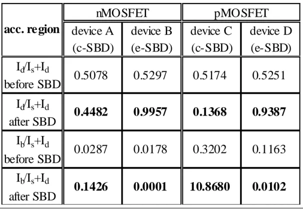
Table 2.1 The ratio of Id/(Is+Id) and Ib/(Is+Id) before and after soft breakdown in
four SOI MOSFETs. The measurement is in the accumulation region
and Vg= |1.5V|, Vd=Vs=0V.
Table 4.1 Calculated distributions of channel holes in the lowest three
sub-bands. The gate bias in simulation is –1.5V. The parameters used
in simulation is m*(Si) = 0.67m0, m*(SiO2) = 0.55m0, φh (hole barrier
height at SiO2 interface) = 4.25eV, tox = 1.6nm, and NB (substrate
Chapter 1
Introduction
Gate oxide thickness scaling has been recognized as one of major keys in CMOS device scaling. With the device shrinkage, gate oxides below 2 nm are needed for sub-100nm CMOS technology. It is amazing that such thin oxide doesn’t suffer much from extrinsic factors such as defect density, surface roughness and uniformity control. The physical limitation of oxide thickness is caused by quantum-mechanical tunneling of carriers. The direct tunneling current increases exponentially by about one order of magnitude for every 2~3Å reduction in oxide thickness [1.1]. Large tunneling currents with device scaling make oxide breakdown play an important role in reliability issues. Additionally, silicon-on-insulator (SOI) CMOS has been emerged as one promising solution to increase the performance of CMOS over that offered by simple scaling.[1.2,1.3] In bulk CMOS, the oxide soft breakdown (SBD) just increases the tunneling leakage current and does not disrupt circuit operation.[1.4] In fact, this unnecessary leakage current not only causes increased power dissipation but also may bring about some reliability subjects such as hysteresis effects, noise degradation and oxide breakdown in ultra-thin oxide SOI CMOS devices.
Partially Depleted (PD) SOI MOSFETs have the advantages in better threshold voltage control and easier fabrication process than fully depleted SOI MOSFETs. However, the floating body configuration of PD SOI MOSFETs has aroused several serious problems in device characteristics. An excess substrate leakage current can charge the substrate and cause annoying hysteresis effects. The SBD enhanced substrate tunneling leakage current may make the hysteresis effects more serious in PD SOI CMOS. The influence of SBD location on hysteresis effects in PD SOI MOSFETs will be investigated in various device operation modes.
analogy circuits due to reduced junction capacitance and also due to the benefits of a high receptivity substrate.[1.5,1.6] Low-frequency noise is a key design constraint and an important figure-of-merit in analogy MOS circuits. Moreover, unwanted floating-body effects including the excess low-frequency noise have been extensively studied for SOI MOSFETs.[1.7,1.8] In this thesis, we will explore the noise properties of PD SOI MOSFETs in different SBD modes. The impact of SBD location on low frequency noise in SOI devices will be investigated in this thesis, too.
Time dependence dielectric breakdown (TDDB) is an important reliability index of ultra-thin gate oxide. Although stress oxide field of SOI MOSFETs is not varied by floating body induced forward substrate bias, the negative substrate bias may enhance the pMOS breakdown progression.[1.9,1.10] The comparison of breakdown hardness in SOI and bulk pMOSFETs will be discussed in this thesis. Our result shows that oxide breakdown rate is enhanced in SOI devices. This points toward that SBD will be an urgent reliability issue in ultra-thin PD SOI MOSFETs.
Organization of This Report
This report is organized into five chapters.
Following the introduction, the impact of oxide soft breakdown location on threshold voltage hysteresis in PD SOI MOSFETs with an ultra-thin oxide is investigated in Chapter 2. Two breakdown enhanced threshold voltage hysteresis modes are identified. In a drain-edge breakdown device, excess holes resulting from band-to-band tunneling flow to the floating body, thus causing threshold voltage variation in drain bias switching. In contrast, in a channel breakdown device, enhanced threshold hysteresis is observed during gate bias switching because of increased valence band electron tunneling. Our findings reveal that soft breakdown enhanced hysteresis effects can be a serious reliability issue in ultra-thin oxide SOI devices with floating body configuration.
In Chapter 3, a new low frequency noise degradation mode in nMOSFETs due to breakdown enhanced floating body effect is proposed. In a channel breakdown device, a noise overshoot phenomenon is observed in the ohmic regime. It is characterized by a peak in drain current noise spectral density versus the operation gate voltage, whereby the peak amplitude can be about one order of magnitude higher than the background 1/f noise. In addition, it is shown that the corresponding spectrum has a Lorentzian shape. The origin of this excess noise is due to c-SBD enhanced valance band electron tunneling induced amplification of the substrate shot noise. The excess low frequency noise model in SOI MOSFETs is also proposed. The findings indicate that c-SBD enhanced drain current noise can be a reliability issue in PD analog SOI CMOS circuit.
In Chapter 4, enhanced oxide breakdown progression in ultra-thin oxide SOI pMOS is observed, as compared to bulk devices. The enhanced progression is attributed to the increase of hole stress current resulting from breakdown induced channel carrier heating in a floating-body configuration. Numerical analysis of hole tunneling current and hot carrier luminescence measurement are performed to support our proposed theory. This phenomenon is particularly significant to the reliability of floating body SOI pMOS with thinner oxides and lower gate voltage. Conclusions are finally made in Chapter 5.
Chapter 2
Soft Breakdown Enhanced Hysteresis Effects in Ultra-Thin Oxide
SOI MOSFETs
2.1 Introduction
Silicon-on-insulator (SOI) technology has emerged as a promising technology for system-on-a-chip applications, which require high-performance complementary metal-oxide-semiconductor (CMOS) field effect transistors (MOSFETs), low power, embedded memory, and bipolar devices. The primary feature of a MOSFET with SOI configuration is that the local substrate of the device is floating electrically, and thus the substrate-source bias (VBS) is not fixed. As VBS changes, the device threshold voltage (Vt) will
change due to the body effect. This “instability” in Vt resulting from floating body
configuration becomes one of the most challenging tasks in bringing SOI devices into mainstream applications.[2.1-2.4] One manifestation of the Vt variation is the hysteresis effect.
The Vt hysteresis as a result of various floating body charging/discharging mechanisms has
been widely investigated.[2.2-2.4] In this work, the influence of gate oxide breakdown position on hysteresis effects in ultra-thin oxide partially-depleted (PD) SOI MOSFETs will be explored.
Several causes of Vt hysteresis in PD SOI MOSFETs have been proposed.[2.5-2.8]
Boudou et al [2.5] reported that Vt hysteresis could be caused by positive feedback of impact
ionization due to long time constants associated with body potential charging. Chen et al [2.6] showed that at high drain biases the floating body effect can lead to hysteresis in the sub-threshold Ids-Vgs characteristics even when the gate is biased well below its threshold
voltage. Fung et al [2.7] found that in ultra thin gate oxide devices the gate-to-body tunneling current modulates the body voltage and induces a hysteresis effect. All the above works investigate the hysteresis phenomenon in PD SOI MOSFETs without considering gate oxide
soft breakdown (SBD). Recent studies [2.9-2.13] showed that in bulk CMOS the impact of gate oxide SBD is only manifested in a noticeable increase in gate leakage current without degrading other device characteristics in operation. Crupi et al [2.14] showed that at high gate voltages the substrate current steeply increases after SBD due to localized effective thinning of gate oxide. Chan et al [2.15] presented that in thinner oxides the post-SBD gate induced drain leakage (GIDL) current increases significantly because of the enhancement of band-to-band tunneling. Although the dependence of these excess substrate currents on the location of a SBD spot was widely explored, the influence of SBD location on Vt hysteresis in
SOI devices has been rarely investigated.
2.2 Device Structure and Characterization
The devices in this work were made with a 0.13µm standard CMOS process on p-type PD SOI substrate. The gate oxide was grown with rapid plasma nitridation (RPN) process. The gate length is 0.13µm, the gate width is 10µm and the oxide thickness is 1.6nm. The test devices have an H-gate structure with an additional contact to facilitate the measurement of the body current and voltage. In this chapter, all devices were stressed at high constant gate voltage with the source and drain grounded. The stress was stopped immediately after the first breakdown was detected. The current compliance for breakdown detection was chosen to be 10µA. After breakdown, the device on-state characteristics were checked and no difference was observed.
The breakdown position was examined by using the method proposed by Degraeve et al.[2.16] Table 2.1 shows the ratio of Id to (Is+Id) before and after SBD in four SOI devices.
The measurement is in accumulation region and |Vg|=1.5V and Vd=Vs=0V. A significant
increase of Id/(Is+Id) in device B and device D indicates that breakdown is located at the drain
2.1). In the channel SBD (c-SBD) devices, the valence band tunneling leakage in the channel region (Ib) was enhanced, resulting in a larger Ib/(Is+Id). In the case of edge SBD (e-SBD), the
breakdown was above the drain edge. As a result, the tunneling leakage current in the channel region remains almost the same as in pre-SBD, and the increased edge leakage current makes Is+Id larger and thus a smaller Ib/(Is+Id). In short, the results in Table 2.1 shows that we can
use the change of Id/(Is+Id) or Ib/(Is+Id) to determine the breakdown location in the channel or
in the drain edge region.
By utilizing the above technique, the device electrical behaviors in c-SBD and e-SBD devices were characterized. In Fig. 2.1, the gate current and the substrate current as a function of Vg in a fresh, a c-SBD, and an e-SBD nMOSFET were compared. The result shows that the
substrate current increases drastically after c-SBD, but has little change after e-SBD. The substrate current at a positive gate bias is attributed to valence electron tunneling from the channel to the gate. The generated holes left behind in the channel then flow to the substrate. This tunneling process is unlikely to occur in the n+ drain region since the valence-band edge of the n+ drain is aligned with the band-gap of the n+ poly-gate. Thus, Ib is enhanced significantly at a positive gate bias in a c-SBD device due to localized effective oxide thinning [2.14, 2.17-2.18] while Ib in an e-SBD device is nearly unchanged. Fig. 2.2 shows the drain
bias dependence of the GIDL current before and after SBD. The substrate current has an apparent increase after edge SBD. This is because at a high drain bias the Ib comes from
electron band-to-band tunneling in the drain depletion region and the generated holes flow to the substrate. Since the electrical field in the drain region becomes stronger after e-SBD due to effectively oxide thinning, the GIDL (Ib) in an e-SBD device is enhanced. The same
2.3 Modes of SBD Enhanced Hysteresis
Two modes of SBD enhanced body potential alteration are proposed. Fig. 2.4 illustrates two floating-body charging processes in c-SBD and in e-SBD SOI nMOSFETs.[2.19-2.20] In a c-SBD device with a positive gate bias (Fig. 2.4(a)), valence band electron tunneling from the channel to the gate is increased after SBD. The generated holes flow to the body and raise the body potential. Fig. 2.4(b) shows the drain-induced floating-body charging in an e-SBD nMOSFET. Since the breakdown path is in the drain edge, the GIDL current increases due to a stronger band bending in the n+ drain region, thus raising the body potential at a high drain bias. On the contrary, the GIDL current does not change in a c-SBD device. Likewise, Fig. 2.5 shows two possible floating-body charging processes in pMOSFETs. Due to the above two charging processes, we conclude that the body potential of both nMOSFET and pMOSFET can be modified either during gate switching or during drain switching depending on the
2.4 Results and Discussion
Fig. 2.6 shows the Ids-Vgs hysteresis in a PD SOI nMOSFET before and after c-SBD. The
measurement drain bias is 0.1V. The gate bias is swept from 0V to 1.3V and then is reversely swept from 1.3 to 0V. Note that (i) the sub-threshold hysteresis before SBD is insignificant and (ii) the post-SBD hysteresis is induced by gate bias sweep in this device. The corresponding body potential fluctuation in gate bias sweep is shown in Fig. 2.6. The arrow in the figure indicates the direction of bias sweep. After c-SBD, the body potential begins to rise when the Vg amplitude is above 0.8V. The gate switching induced body potential variation can
be as large as 0.3V in this case. The pre-SBD body potential hysteresis at the same switching amplitude is less than a few tens of milli-volts. The c-SBD induced Vt hysteresis is also
observed in a pMOSFET. The measurement data are not shown here.
In an e-SBD device, although gate enhanced hysteresis is not observed, drain sweep induced hysteresis in sub-threshold leakage current is remarkable (Fig. 2.7). In this figure, the measurement Vgs is 0V and the drain bias is swept from 0V to 1.3V and then reversely swept
back. The body potential variation is shown in Fig. 2.7, too. The e-SBD enhanced hysteresis effect is clearly shown in this figure. It should be noted these breakdown-induced hysteresis effects occurs in off-state rather than in on-state where hot carrier impact ionization has been reported as a responsible charging mechanism.[2.5]
The relationship between the magnitude of sweep voltage and the body potential hysteresis in the two SBD modes is investigated. In nMOSFETs, the degree of hysteresis in terms of the body potential variation versus the amplitude of the sweep voltage is shown in Fig. 2.8 for gate bias sweep and in Fig. 2.9 for drain bias sweep. The hysteresis voltage is defined as the maximum substrate charging voltage during the sweep. In gate bias sweep (Fig. 2.8), the c-SBD device shows an increased hysteresis voltage while the hysteresis voltage of the e-SBD device is almost unchanged. In contrast, the e-SBD device shows a larger hysteresis voltage in drain bias sweep (Fig. 2.9). Similar results in pMOSFETs are presented
in Fig. 2.10 for gate bias sweep and in Fig. 2.11 for drain bias sweep. From our characterization, we found SBD induced hysteresis effect may become appreciable even when the supply voltage is below 0.8V.
The impact of SBD enhanced body charging effect in CMOS operation is described as follows. Fig. 2.12 illustrates the dominant Vt hysteresis modes in a SOI CMOS inverter. Hot
carrier (HC) induced floating body charging occurs in on state [2.1,2.5] and it is dominant only when the inverter is during switching. On the other hand, floating body charging takes place in c-SBD (e-SBD) nMOSFETs and e-SBD (c-SBD) pMOSFETs when the input signal is at high (low) state. Since the soft breakdown induced body charging is in the off state, the time for charging can be much longer than the on-state HC caused body charging. Our study reveals that SBD in PD SOI MOSFETs not only increases leakage current but also affects circuit stability.
2.5 Summary
The significance of soft breakdown position to Vt hysteresis in PD SOI CMOS devices
has been evaluated. Two SBD enhanced hysteresis modes in off-state CMOS are identified. The dominant floating body charging mechanism is valence band tunneling in c-SBD devices and band-to-band tunneling in e-SBD devices. The SBD enhanced hysteresis effect may occur even with supply voltage less than 1.0V and would be a serious reliability concern in ultra-thin oxide PD SOI circuits.
device A
(c-SBD)
device B
(e-SBD)
device C
(c-SBD)
device D
(e-SBD)
I
d/I
s+I
dbefore SBD
0.5078
0.5297
0.5174
0.5251
I
d/I
s+I
dafter SBD
0.4482
0.9957
0.1368
0.9387
I
b/I
s+I
dbefore SBD
0.0287
0.0178
0.3202
0.1163
I
b/I
s+I
dafter SBD
0.1426
0.0001
10.8680
0.0102
nMOSFET
pMOSFET
acc. region
Table 2.1 The ratio of Id/(Is+Id) and Ib/(Is+Id) before and after soft breakdown in
four SOI MOSFETs. The measurement is in the accumulation region and Vg=
0 0.5 1 1.5 2
10
-5
10
-7
10
-9
10
-11
Gate bias (volts)
Current (Amp)
fresh
post c-SBD
post e-SBD
Gate
current
Substrate
current
V
d
=0V
Fig.2.1 Gate current and substrate current versus gate bias in nMOSFETs. Solid line refers to an unstressed device and dashed line (dotted line) refers to a device after channel SBD (drain edge SBD).
0 0.5 1 1.5 2
10
-7
10
-9
10
-11
Drain bias (volts)
Body current (Amp)
fresh
post c-SBD
post e-SBD
V
g
=0V
Fig.2.2 Body current versus drain bias in nMOSFETs. Solid line refers to an unstressed device and dashed line (dotted line) refers to a device after channel SBD (drain edge SBD).
10
-5
10
-7
10
-9
10
-11
Gate bias (volts)
Current (Amp)
fresh
post c-SBD
post e-SBD
Gate
current
Substrate
current
V
d
=0V
-2 -1.5 -1 -0.5 0
Fig.2.3 Gate current and substrate current versus gate bias in pMOSFETs. Solid line refers to an unstressed device and dashed line (dotted line) refers to a device after channel SBD (drain edge SBD).
n
+
n
+
+V
gvalence-band
tunneling
n
+
n
+
+V
dband-to-band
current
(a)
(b)
Fig.2.4 Illustration of two soft-breakdown enhanced floating-body charging processes in SOI nMOSFETs. (a) soft breakdown in the channel region and hole creation due to valence band electron tunneling; (b) soft breakdown in the drain region and enhanced GIDL current.
p
+
p
+
V
gvalence-band
tunneling
p
+
p
+
-V
dband-to-band
current
(a)
(b)
+
+
-V
gvalence-band
+
+
V
dband-to-band
(a)
(b)
Fig.2.5 Illustration of two soft-breakdown enhanced floating-body charging processes in SOI pMOSFETs. (a) soft breakdown in the channel region and valence band electron tunneling from poly-gate to the floating body; (b) soft breakdown in the drain region and
0.5
0.4
0.3
0.2
0.1
0
0 0.5 1 1.5
10
-2
10
-4
10
-6
10
-8
10
-10
Gate bias (volts)
Drain to source current (Amp)
pre c-SBD
post c-SBD
Body voltage (volts)
V
d
=0.1V
Fig.2.6 Hysteresis in Ids and corresponding floating-body potential versus Vg in a
c-SBD SOI nMOSFETs. Measurement is performed with forward and then reverse drain sweeps from 0V to 1.3V.
0 0.5 1 1.5
10
-6
10
-7
10
-8
10
-9
Drain bias (volts)
Drain to source current (Amp
)
pre e-SBD
post e-SBD
V
g
=0V
0.5
0.4
0.3
0.2
0.1
0
Body voltage (volts)
Fig.2.7 Hysteresis in sub-threshold current and corresponding floating-body potential in an e-SBD SOI nMOSFETs. Measurement is performed with forward and then reverse drain sweeps from 0V to 1.3V.
0 0.5 1 1.5
0.5
0.4
0.3
0.2
0.1
0
Max. sweep gate bias (volts)
Hysteresis
voltage, V
b
(volts)
fresh
post c-SBD
post e-SBD
V
d
=0V
Fig.2.8 The variation of body voltage Vb as a function of the amplitude of gate
0 0.5 1 1.5
Max. sweep drain bias (volts)
Hysteresis
voltage, V
b
(volts)
fresh
post c-SBD
post e-SBD
V
g
=0V
0.5
0.4
0.3
0.2
0.1
0
Fig.2.9 The variation of body voltage Vb as a function of the amplitude of drain
Max. sweep gate bias (volts)
Hysteresis
voltage, V
b
(volts)
-1.5 -1 -0.5 0
fresh
post c-SBD
post e-SBD
V
d
=0V
-0.5
-0.4
-0.3
-0.2
-0.1
0
Fig.2.10 The variation of body voltage Vb as a function of the amplitude of gate
-1.5 -1 -0.5 0
Max. sweep drain bias (volts)
Hysteresis
voltage, V
b
(volts)
fresh
post c-SBD
post e-SBD
V
g
=0V
-0.5
-0.4
-0.3
-0.2
-0.1
0
Fig.2.11 The variation of body voltage Vb as a function of the amplitude of drain
V
out
V
in
V
out
V
cc
GND
V
in
c-SBD
e-SBD
V
out
V
in
V
out
V
cc
GND
V
in
V
out
V
cc
GND
V
in
c-SBD
e-SBD
HC
c-SBD
c-SBD
e-SBD
e-SBD
Fig.2.12 Illustration of dominant Vt hysteresis modes in the switching of an SOI
Chapter 3
Soft Breakdown Enhanced Excess Low-Frequency Noise in
Ultra-Thin Oxide SOI n-MOSFETs
3.1 Introduction
Silicon-on-insulator (SOI) technology also has regarded as a hopeful technology for system-on-a-chip applications, which require high-performance, low power, fully integrated RF, and mixed-signal circuits.[3.1-3.5] However, the troublesome floating-body effect (FBE) in PD SOI MOSFETs leads to kink in drain current characteristics as well as some undesirable transient effects.[3.1-3.4] FBE also gives rise to excess low-frequency noise with a Lorentzian-like spectrum in floating body PD SOI devices, posing a serious problem for base band signal processing system.[3.6-3.9] The observed Lorentzian shaped noise is caused by white thermal noise (Nyquist or shot) sources associated with the generation and removal of body charge.[3.6] The Lorentzian signature is obtained through the trans-impedances coupling these internal white noise sources to the terminals of the SOI device.[3.7] Several causes of the Lorentzian-like spectrum in SOI MOSFETs have been proposed. The origin of these floating body noises could be related to high drain bias induced impact ionization current and large gate bias induced valance band electron tunneling through the ultra-thin gate oxide.[3.9-3.10] Chapter 3 has pointed out that soft breakdown enhanced substrate tunneling current would induce threshold voltage (Vt) hysteresis effects in PD SOI MOSFETS.[3.11]
The aim of this chapter is to describe the impact of soft breakdown location on the excess low-frequency noise for SOI devices with floating body configuration.
In the beginning, the excess noise model in PD SOI MOSFETs is introduced. Then, the kink effect in ultra-thin oxide floating body SOI n-MOSFETs is studied, which would induce excess low frequency noise. After that, the impact of soft breakdown location on drain current
noise overshoot phenomenon is observed in the ohmic regime. It is characterized by a peak in current noise spectral density versus the operation gate voltage, whereby the peak amplitude can be about one order of magnitude higher than the background flicker noise. The origin of this excess noise is believed due to soft breakdown (SBD) enhanced valance-band electron tunneling and thus induced floating body effect. The findings indicate that channel SBD enhanced drain current noise can be a reliability issue in PD analog SOI CMOS circuit.
3.2 Excess Low-Frequency Noise Model in SOI MOSFETs
The major noise sources of an SOI MOSFETs operating in strong inversion are shown in Fig. 3.1. There are two noise sources associated with the conducting channel. One is flicker (1/f) noise which contributes to the low-frequency noise, the other is thermal noise which dominates at high frequency. In addition to the noise in the channel, there are two shot noise sources associated with the floating-body, which are due to the impact ionization current and the body-source diode current, respectively. In bulk MOSFET, only 1/f noise can be observed at low-frequency. However, excess noise is found in floating-body PD SOI MOSFET. The excess noise originates in the two shot noises. Although the shot noises are small in magnitude compared with flicker noise, they are amplified by FBE and give rise to the excess low-frequency noise in PD SOI MOSFET. The low-frequency noise in floating-body PD SOI MOSFET’s includes white noise, flicker noise and the FBE-induced excess noise.
A. White Noise
The white noise component originates from thermal random motion of carriers in the channel.
.
B. Flicker Noise
1/fβ, where β is close to unity so that flicker is normally called 1/f noise. There is no consensus to the origin of the 1/f noise, it is very likely that there exist more than one mechanism giving rise to the same noise characteristics. According to McWhorter’s number fluctuation theory [3.12], 1/f noise is attributed to the trapping and de-trapping processes of the charges in the oxide traps close to the Si–SiO2 interface. Hooge’s empirical model [3.13],
however, considers the 1/f noise as a result of carrier mobility fluctuation due to lattice scattering. It has been reported that both the carrier number fluctuation and the mobility fluctuation are possible mechanisms which lead to the 1/f noise in MOSFET’s [3.14-3.15]. Hence, for the 1/f noise, a correlated noise model [3.14] which incorporates both mechanisms is applied
∫
+ = − ds V eff f t eff eff ds f id N dV N E N fL kTqI S 0 2 2 / 1 (1 ) ) ( αµ γ µ (3.1) whereSid-1/f 1/f noise current spectral density;
Ids drain current;
µeff effective mobility;
γ attenuation coefficient of the electron wave function in the oxide; Leff effective channel length of the device;
Vds drain bias;
Nt(Ef) oxide trap concentration around the quasi-Fermi level along the channel;
N carrier concentration along the channel; α lattice scattering coefficient.
The excess low-frequency noise is specific to PD SOI MOSFET’s associated with the floating-body effect (FBE). The noise small-signal equivalent circuit shown in Fig. 3.2(a) can explain the mechanism underlying the excess low-frequency noise [3.6]. The shot noise results from the impact ionization current (Iii):
ii ib M qI
S 1 = ⋅2 (3.2)
where M is a multiplication factor [3.16]. Impact ionization current exhibits shot noise because only the carriers with sufficient kinetic energy can generate electron-hole pairs. The second noise source is associated with the body-source diode current (Ibs) where carriers have
to overcome the built-in potential barrier:
bs ib qI
S 2 =2 (3.3)
The two noise current flow through the body-ground impedance ( and ), leading to a fluctuation in body potential:
eq c req 2 1 2 | ) 1 ( | | | = ⋅ + − ⋅ = eq eq ib b ib vb j c r S z S S ω
2 2 ) ( 1 eq ib f f r S + ⋅ = c (3.4) where 2 1 ib ib ib S S S = + and eq eq c c r f ⋅ = π 2 1
The equivalent body-ground resistance is equal to the small-signal resistance of the body-source junction. The equivalent body-ground capacitance can be modeled as the sum of all the capacitance seen from the body. The schematic for and is shown in Fig. 3.2(b). And, the fluctuation in the body potential modulates the threshold voltage of the device: eq r eq c eq r ceq 2 ) ( bs th vb vth V V S S ∂ ∂ ⋅ = (3.5)
Due to the fluctuation in Vth, the excess drain current noise is given by:
2 ) ( th ds vth excess id V I S S ∂ ∂ ⋅ = − 2 2 2 ) ( 1 2 ) 1 ( ii mb eq f f r g qI M + ⋅ + = c
(3.6)
where gmb is the body trans-conductance. The excess noise shows a Lorentzian power
spectrum, which is characterized by a constant plateau at low frequency and a 1/f 2 roll-off at higher frequencies.
Since white noise, 1/f noise and excess noise are uncorrelated, the total spectrum density of low-frequency drain current noise is the sum of the three components (Fig 3.3):
white id excess id f id total id S S S S − = −1/ + − + − (3.7)
To verify the proposed low-frequency noise model, the noise measurement is conducted according to the setup shown in Fig. 3.4. The DC bias to the DUT is supplied by the Berkeley Technology Associate BTA9603 Noise Analyzer, which eliminates the residual noise in the bias voltages generated by HP4155C Semiconductor Parameter Analyzer. The noise current of the DUT is amplified by the low-noise amplifiers in BTA9603 before being applied to the Stanford Research SR780 Network Signal Analyzer (bandwidth: dc to 100 kHz) for FFT (fast Fourier transform). A computer installed with Noise Pro is used to automatically control the whole measurement.
3.3 Kink Effect Induced Excess Low-Frequency Noise
The SOI devices in this chapter were made with a 0.13µm standard CMOS process on p-type silicon substrate. Fig. 3.5 shows ours measured Id-Vd characteristics of SOI
n-MOSFETs (W/L = 10μm/0.18μm) with floating body and grounding body. Gate is biased at 0.9V. The kink effect is obviously observed in a floating body n-MOSFET and not in an n-MOSFET with body grounded. Due to the impact ionization current, electron-hole pairs are created at the drain end. Then, the holes go to the floating body, which induce the variation of body potential. At the kink point where the body potential sufficiently increases, threshold voltage drops and thus causes an increase of the drain current. The phenomenon in the floating body n-MOSFET consists with others results in PD SOI MOSFETs.[3.6] The excess noise is also found in floating body PD SOI MOSFET as the drain bias is above the kink voltage.
In Fig. 3.6, normalized noise power spectrum density in an n-MOSFET with body floated is measured at gate biased 0.9 V, and drain biased 0.5V、1.0V、1.2V、1.3V、1.4V、 1.6V. Fig. 3.6 shows that the excess noise is not observable in the curve corresponding to the linear regime operation. As drain biases is above the kink onset voltage, the normalized noise power spectrum exhibits a plateau up to the characteristic frequency fc = 1/(2π⋅reqceq) before a 1/f2 roll-ff sets in. Furthermore, a typical Lorentzian shift to lower plateau and higher cut-off frequency is observed due to the increase of impact ionization current with the drain bias. Because the decreases with increasing drain voltage, a larger drain bias gives rise to a higher f
eq
r
c but a smaller noise magnitude.
Additionally, Fig. 3.7 shows that normalized noise power spectrum density in an n-MOSFET with body grounded. Fig. 3.7 manifests that only flicker noise is exhibited at drain biased from linear regime to saturation regime. That is, the excess noise can be effectively eliminated, as body contact is grounded. Fig. 3.8 illustrates that the normalized
point appears for a given frequency. This is when the device switches from linear operation regime to the regime around the kink point with the increase of the drain voltage.
The low-frequency noise in floating-body PD SOI MOSFETs is composed of 1/f noise and shot noise-induced excess noise. High drain bias gives rise to impact ionization current which flows through the floating-body to the source terminal. The shot noise causes fluctuation of body potential and threshold voltage, and consequently leads to excess noise in drain current. The RC network of the body in floating-body PD SOI MOSFETs amplifies and filters the shot noise, giving rise to a Lorentzian-like spectral density in noise. The noise peaks around the kink onset voltage for a given frequency. These experimental results consisted with previous mentioned noise model.
3.4 Channel Soft Breakdown Enhanced Excess Low-Frequency Noise
The gate length of this section is 0.13µm, the gate width is 10µm and the oxide thickness is 1.6nm. All devices were stressed at high constant gate voltages with the source and drain grounded. The stress was stopped immediately after the first breakdown was detected. The current compliance for breakdown detection was chosen to be 10µA. After breakdown, the device on-state characteristics were checked and no difference was observed. Similarly, from others’ study, [3.17-3.21] the impact of the gate oxide SBD is only a noticeable increase in leakage current without degrading any on-state device performance in operation.
The breakdown position was examined by using the method given in Chapter 2.[3.22] The measurement gate bias is Vg=-1.5V and Vd=Vs=0V in the accumulation region. A
significant increase of Id/Is+Id in device indicates that breakdown is located at the drain edge,
while the moderate change in Id/Is+Id implies that SBD position is in the channel. By utilizing
the aforementioned technique of examining the breakdown location, the device electrical behaviors before and after various soft breakdown modes could be characterized. In Fig. 4.9, the gate current and substrate current as a function of Vg in fresh, channel-SBD, and
edge-SBD n-MOSFETs were compared.
This comparison indicates that the substrate current increased drastically in channel-SBD devices, but the change in edge-SBD devices was negligible. The substrate current at a positive gate bias is attributed to channel hole creation resulting from valence-band electron tunneling from Si substrate to the conduction band of the poly gate. The tunneling process is unlikely to occur in the n+ drain region since the valence-band edge of the n+ drain is aligned with the band-gap of the n+ poly-gate. Thus, these findings support the viewpoint that the post c-SBD Ib is enhanced largely at a positive gate bias due to a localized effective oxide thinning
[3.23-3.25] while Ib is nearly unchanged after e-SBD. The results provide direct experimental
According to the above results, c-SBD enhanced substrate tunneling current in PD SOI MOSFETs is proposed as a new body-charging mode.[3.11,3.26-3.27] To further illustrate this point; the low frequency drain noise spectrums of SOI nMOSFET before and after both SBD modes are shown in Fig. 3.10. The measurement drain bias is 0.1V and the gate bias is 1.2V. The pre-BD noise characteristics of 1.6 nm gate oxide nMOSFET were dominated by a 1/f-like flicker noise component without other noise component of linear kink effect.[3.28] Suitable channel engineer process can eliminate the excess floating body noise of SOI device in advanced 0.13µm generation SOI technologies.[3.8,3.10] An additional Lorentizian-like spectrum appears only when both channel soft breakdown occurs and body contact is floated. As body contact is grounded, the excess noise can be effectively eliminated. The excess noise is also not observable in e-SBD devices. It indicates that the additional body charge injection of c-SBD devices not only enhances the Vt hysteresis effect but also degrades the LF noise
spectrum.
Now, we would further investigate the gate bias dependence of the c-SBD induced excess floating body noise. Fig. 3.11 shows the normalized noise spectra of a floating body c-SBD SOI nMOSFETs under different gate biases. We observed a typical Lorentzian shift to lower plateau and higher cut-off frequency due to the valance band electron current increase with the gate bias. At Vg=1.6V, only 1/f noise is observed. In fact, we believe there is still a
Lorentzian in this case but shifted to lower frequency, below our measurement capability. Note that the normalized 1/f noise remains almost constant over measurement gate bias in this ohmic region. This could be associated with the number fluctuation dominated in this measurement.[3.29-3.30] The excess noise of a c-SBD SOI devices with floating body shows similar behaviors to the excess noise induced by the kink effect in section 3.3.
Fig. 3.12 illustrates that for a given frequency, the normalized drain current noise of c-SBD floating body SOI devices initially increases with Vg and reaches a peak when gate
the body in floating-body PD SOI nMOSFET’s amplifies and filters the shot noise of substrate current, giving rise to a Lorentzian-like spectral density in noise.[3.6-3.9] It can be explained that with an increase in gate voltage, c-SBD induces more substrate current as a result of valance band electron tunneling. Further increase in gate bias leads to a low amplification gain by the floating-body to the shot noise, because the equivalent substrate resistance decreases with the substrate current increase, thus the noise magnitude decreases.[3.7]
3.5 Summary
The significance of soft breakdown position to the low frequency drain current noise in floating body PD SOI nMOSFETs has been evaluated. The excess floating body noise of nMOSFETs would be enhanced if a breakdown path occurs at the channel. The enhanced noise correlates with channel soft breakdown induced large substrate current of valance band electron tunneling. This noise sources origins from the amplification by small white noise of the substrate current. The c-SBD enhanced excess noise may occur even with supply voltage less than 1.0V and would be a serious reliability concern in ultra-thin oxide analog SOI devices.
Gate
Drain
Source
Body
i
f2i
t2i
ii2i
bs2i
f2i
t 2i
ii2i
bs2:Flicker Noise :Thermal Noise
:Shot Noise due to body-source diode current
:Shot Noise due to impact ionization current
Gate
Drain
Source
Body
i
f2i
t2i
ii2i
bs2Gate
Drain
Source
Body
i
f2i
f2i
t2i
t2i
ii2i
ii2i
bs2i
bs2i
f2i
f2i
t 2i
t2i
ii2i
ii2i
bs2i
bs2:Flicker Noise :Thermal Noise
:Shot Noise due to body-source diode current
:Shot Noise due to impact ionization current
Body
Ground
i
ii2i
bs2C
eqr
eqSource
Gate
Drain
Cjs Cjd Cbb Cbe rjsi
ii2i
bs 2= 2qI
iiB, = 2qI
bsB
B: noise band width
C
bb: body to channel depletion cap.
C
js/jd: body to S/D junction cap.
R
js: body to source AC resistance
r
eq= r
js, C
eq= C
bb+ C
be+ C
js+ C
jdBody
Ground
i
ii2i
bs2C
eqr
eqSource
Gate
Drain
Cjs Cjd Cbb Cbe rjsBody
Ground
i
ii2i
ii2i
bs2i
bs2C
eqr
eqSource
Gate
Drain
Cjs Cjd Cbb Cbe rjsSource
Gate
Drain
Gate
Drain
Cjs Cjd Cbb Cbe rjsi
ii2i
bs 2= 2qI
iiB, = 2qI
bsB
B: noise band width
i
ii2i
ii2i
bs 2i
bs2= 2qI
iiB, = 2qI
bsB
B: noise band width
C
bb: body to channel depletion cap.
C
js/jd: body to S/D junction cap.
R
js: body to source AC resistance
r
eq= r
js, C
eq= C
bb+ C
be+ C
js+ C
jd(a)
(b)
Fig.3.2 (a) Noise small-signal equivalent circuit for the floating-body and (b) schematic for the req and Ceq network.
Power
Spectral
Density
(log)
frequency (log)
1/f noise
plateau
Lorentzian
white noise
1/f
2
corner frequency
Power
Spectral
Density
(log)
frequency (log)
1/f noise
plateau
Lorentzian
white noise
1/f
2
corner frequency
BTA 9603 FET Noise Analyzer
D G B S V
D
V
G
V
B
V
S
S
Id
Device
Under
Test
HP 4155C
Semiconductor
Parameter
Analyzer
SR 780
Dynamic
Signal
Analyzer
BTA 9603 FET Noise Analyzer
D G B S V
D
V
G
V
B
V
S
S
Id
Device
Under
Test
HP 4155C
Semiconductor
Parameter
Analyzer
SR 780
Dynamic
Signal
Analyzer
0.0
0.5
1.0
1.5
0.0
2.0x10
-44.0x10
-46.0x10
-4I
d
(Amp)
V
d
(volts)
W/L=10
µm / 0.18
µm
V
g=0.9V
V
b=0V
V
b=floating
Fig.3.5 The Id-Vd characteristics in nMOS SOI devices with floating body and
10
010
110
210
310
410
510
610
-1510
-1310
-1110
-9S
Id
/Id
2
(1/Hz)
frequency (Hz)
V
g=0.9V V
b=floating
V
d=0.5V
V
d=1.0V
V
d=1.2V
V
d=1.3V
V
d=1.4V
V
d=1.6V
Fig.3.6 Normalization noise power spectral density in floating body nMOS SOI devices under different drain voltage when gate is biased at 0.9V.
10
010
110
210
310
410
510
610
-1510
-1310
-1110
-9S
Id
/Id
2
(1/Hz)
frequency (Hz)
V
g=0.9V V
b=0V
V
d=0.5V
V
d=1.0V
V
d=1.2V
V
d=1.4V
V
d=1.6V
Fig.3.7 Normalization noise power spectral density in grounding body nMOS SOI devices under different drain voltage when gate is biased at 0.9V.
0.4
0.6
0.8
1.0
1.2
1.4
1.6
10
-1310
-1210
-1110
-10 float @100Hz bulk @100Hz float @1KHz bulk @1KHzS
Id
/Id
2
(1/Hz)
V
d
(volts)
Fig.3.8 Comparison of normalization noise power spectral density under different drain bias in floating body SOI devices and grounding body SOI devices for given frequency.
0 0.5 1 1.5 2
10
-5
10
-7
10
-9
10
-11
Gate bias (volts)
Curren
t (Am
p
)
fresh
post c-SBD
post e-SBD
Gate
current
Substrate
current
V
d=0V
0 0.5 1 1.5 2
10
-5
10
-7
10
-9
10
-11
Gate bias (volts)
Curren
t (Am
p
)
fresh
post c-SBD
post e-SBD
Gate
current
Substrate
current
V
d=0V
Fig.3.9 The gate current and substrate current as a function of Vg in fresh,
10
010
110
210
310
410
510
-1410
-1310
-1210
-1110
-1010
-910
-8 fresh_ Vb=ground fresh_ Vb=floating c-SBD_ Vb=ground c-SBD_ Vb=floating e-SBD_ Vb=ground e-SBD_ Vb=floatingS
Id
/Id
2
f
frequency (Hz)
S
Id
/Id
2
(1
/Hz
)
10
010
110
210
310
410
510
-1410
-1310
-1210
-1110
-1010
-910
-8 fresh_ Vb=ground fresh_ Vb=floating c-SBD_ Vb=ground c-SBD_ Vb=floating e-SBD_ Vb=ground e-SBD_ Vb=floatingS
Id
/Id
2
f
frequency (Hz)
S
Id
/Id
2
(1
/Hz
)
Fig.3.10 The low frequency drain noise spectrums of n-MOSFET before and after both SBD modes are shown. The measurement drain bias is 0.1V and the gate bias is 1.2V.