國 立 交 通 大 學
光 電 工 程 研 究 所
碩士論文
氮化鎵面射型雷射製程技術之研究
Study of Fabrication Techniques for GaN based VCSEL
研
研
究
究
生
生
:
:
高
高
宗
宗
鼎
鼎
..指
指
導
導
教
教
授
授
:
:
王
王
興
興
宗
宗
教
教
授
授
郭
郭
浩
浩
中
中
教
教
授
授
中
中
華
華
民
民
國
國
九
九
十
十
五
五
年
年
六
六
月
月
氮化鎵面射型雷射製程技術之研究
研究生: 高宗鼎 指導教授: 王興宗 教授,郭浩中 教授 國立交通大學 光電工程研究所摘 要
本論文主要是探討兩種改善氮化鎵微共振腔元件特性的製程技術。以期能夠成功製 作出電激發氮化鎵面射型雷射。其中一種改善的方法是用 ITO 來取代過去氮化鎵微共振 腔元件的 Ni/Au 薄金屬透明電極.我們首先利用模擬軟體來計算出 ITO 所需的厚度並充 分運用各種半導體製程技術,諸如:蝕刻、薄膜成長、歐姆接觸電極之蒸鍍等…,成功 的製作出利用 ITO 作為透明電極的氮化鎵微共振腔元件。此一元件在室溫 10 毫安培的 電流注入下,發光波長在 458nm,並具有一窄的光譜半高寬值為 2nm。由此元件的光學 特性可以計算出此元件的 Q 值已經由過去元件的 68 增加到 229.此結果告訴我們在製作 high Q 的光學元件時,透明電極的吸收率扮演著極重要的角色。除此之外,我們也針對 元件發光孔內的亮點去做探討。可以發現這些亮點相對於其他區域都有著比較高的 Q 值。並且在其中一處發現了 Q 值高達 894 的亮點。由雷射理論我們可以推斷出這些亮點 是由於氮化鎵/鋁化鎵布拉格反射鏡的不均勻造成的。另外一個製程技術是利用鎂離子 佈值在 p 型氮化鎵來取代過去利用氮化矽絕緣層作為電流侷限的方法。我們首先利用模 擬軟體來設計鎂離子佈值的能量及所需的氮化矽緩衝層的厚度。並且由二次離子質譜儀 的結果來加以確定。從元件進行複合式結構的氮化鎵面射型雷射之設計。由元件發光的 情形可以看出我們徹底解決了過去利用氮化矽絕緣層所造成的漏電流的問題。上述兩種 製程技術的改善說明了其發展電激發氮化鎵面射型雷射之可行性與潛力。Study of Fabrication Techniques for GaN-based VCSEL
Student : Tsung-Ting Kao Advisor : Dr. S.C. Wang Dr. H.C. Kuo
Institute of electro-optical Engineering National Chiao-Tung University
Abstract
In this thesis, we investigate the performance of GaN based micro-cavity light emitting diode (MCLED) with two fabrication techniques for the realization of electrically injected GaN VCSEL. One of the techniques is the use of high-transmittance transparent contact, ITO film. The device shows the turn on voltage is a comparable value with Ni/Au device to be about 3.4V and 530Ω, respectively. The emission peak wavelength of the ITO MCLED was located at 458nm with a narrow line-width of 2nm. Compared to the emission spectrum of the conventional Ni/Au MCLED, the ITO MCLED shows a relatively excellent line-width and possesses a high Q factor of about 229. The improvement of Q factor shows that the non-absorbed transparent contact indeed plays an important role to fabricate this kind of high Q device like VCSEL. Moreover, the “bright spots” within the emission aperture were also discussed. We found the Q factors at the bright spots are relatively higher than those within the dark regions, even as high as 894. The excellent Q factor is the best value compared with that of MCLED published in the recent literatures. The other technique is current confinement using Mg ion implantation. The device is implanted by 80keV Mg with does of 2E15. Moreover, 100nm thick SiNx as buffer layer is required for avoiding damage induced defect in MQWs. The absence of side wall emission of implanted MCLED not only confirms the existence of leakage current in our conventional device but also verifies the current confinement was successful. Such techniques could be the basis for electrically injected GaN-based VCSEL.
誌謝
歲月匆匆,碩士生涯一晃眼就要結束了,回想當初憑著一股對光源充滿興趣的傻勁 而選擇念光電所並進入半導體雷射實驗室,我很慶幸當初的選擇,因為在這裡的兩年 中,是我自求學以來收穫最多的一個階段。 首先要感謝王興宗老師的敦敦教誨,王老師對學問表現出來的熱忱與執著,深深的 影響了我的求學態度,也是我未來面對困難時最好的典範。再來要感謝郭浩中老師的帶 領,給我明確的研究方向,並且時時給予我支持與鼓勵。也要感謝盧廷昌老師在我論文 上的建議與指導,還有黃博和姚忻宏學長在磊晶上的協助。特別要感謝常被我調侃的直 屬學長小強,謝謝你全心全力的付出與指導,不僅讓我的論文順利完成,更使我學到很 多待人接物的道理,也希望你未來能夠順順利利。此外,感謝小朱、道鴻、亞銜、泓文、 宗憲、小賴、裕鈞、文燈、傳煜、瑞溢、國峰等學長與芳儀和乃方學姐在實驗上給我的 協助與寶貴的建議。也謝謝助理麗君在行政業務上的幫忙。此外,我要感謝清大物理所 的建旭學長在離子佈值實驗上的幫忙,謝謝你無條件的指導,讓我能了解很多原子物理 方面的知識。幸運如我,能在老師和學長的指導下,有幸能參與台灣第一顆光激發雷射 的誕生,謝謝你們帶給我的驚喜與歡樂,相信我已成長不少。 此外,感謝和我一起努力兩年的同學文凱、剛帆、皇伸、柏傑、意偵、志堯和游敏, 謝謝你們總是能在我研究期間失落的時候給我鼓勵,很高興能夠認識你們,希望未來大 家還能夠常常連絡,也很謝謝學弟妹金門、孟儒、潤琪、家璞、瑞農、卓奕、碩均和秉 寬的幫忙,也祝福你們未來在研究上都能順順利利的。 最後,我要感謝我親愛的父母與哥哥,還有我的女友和所有家人,謝謝你們無怨無 悔的付出與全心全力的支持,使我能順利的完成研究。希望我沒讓你們失望。 2006/07 宗鼎于Contents
Abstract (in Chinese)...i
Abstract (in English)...ii
Acknowledgement...iii Contents...iv Table Contents...vi Figure Contents...vii Chapter 1 Overview………..1 1.1 Introduction………1
1.2 GaN-based Surface Emitting Devices………2
1.3 Objective of the Thesis………...2
1.4 Outline of the Thesis………...3
Chapter 2 Fundamentals of VCSEL and Fabry-Perot Resonator………4
2.1 Introduction to VCSELs………....4
2.2 The Theory of DBRs……….7
2.3 Febry-Perot Resonator……….11
2.4 The Finesse and the Quality Factor of Resonant Cavity……….12
2.5 Operation Mechanism of VCSEL………....13
2.6 Work Review………...19
Chapter 3 Fundamentals of Ion Implantation...22
3.1 Introduction to Ion Implantation...22
3.2 Principle of Ion Implantation...23
Chapter 4 GaN based MCLEDs using ITO as transparent contact layer...28
4.1 Recent Status...28
4.1.1 Introduction to Conventional GaN based MCLED...28
4.1.2 Issue of Q factor...28
4.2 GaN based MCLED using ITO as transparent contact layer...30
4.2.1 Introduction to indium tin oxide (ITO)...30
4.2.3 Comparison of the absorption coefficient of ITO and Ni/Au
film...31
4.3 Fabrication of GaN based MCLED using ITO as transparent contact layer...33
4.3.1 Wafer Preparation...33
4.3.2 Process Procedure...36
4.4 Characteristics of GaN-based MCLED using ITO as transparent contact layer...40
4.4.1 Electrical Characteristics of ITO MCLED...40
4.4.2 Optical Characteristics of ITO MCLED...42
4.5 Inhomogeneities in the device...43
4.6 Summary...46
Chapter 5 Mg+ ion implantation for current confinement in GaN-based Micro-cavity Light Emitting Diodes (MCLEDs) ...47
5.1 Recent Status...47
5.2 Simulation Design and SIMS results of Mg+ ion implantation in GaN....48
5.2.1 Introduction to TRIM simulation software...48
5.2.2 Introduction to Secondary Ion Mass Spectrometer (SIMS)...49
5.2.3 TRIM Simulation and SIMS results of ion implantation...50
5.3 Fabrication of GaN-based MCLED using Mg+ ion implantation for current confinement ...52
5.3.1 Process Procedure...52
5.4 The characteristics of GaN based MCLED using Mg+ ion implantation for current confinement...56
5.4.1 The electrical characteristics measurement setup...56
5.4.2 The emission image of implanted and conventional device...56
5.4.3 The I-V curves of implanted and conventional device...58
5.5 Summary...59
Chapter 6 Conclusions...60
Table Contents
Table 4.1 Process flowchart of MCLED using ITO as transparent contact layer...39 Table 5.1 Process flowchart of MCLED using Mg+ ion implantation for current confinement...55
Figure Contents
Fig. 2.1 Schematic diagrams of (a) an EEL and (b) a VCSEL...4 Fig. 2.2 Typical structures of VCSEL and DBRs...5 Fig. 2.3 Schematic diagram of the light reflected from the top and bottom of the thin film...7 Fig. 2.4 Schematic diagram of DBRs...9 Fig. 2.5 A schematic diagram of a Fabry-Perot cavity with two metallic reflectors with reflectivity R1 and R2...11 Fig. 2.6 The transmission pattern of a Fabry-Perot cavity in frequency domain...13 Fig. 2.7 Reservoir with continuous supply and leakage as an analog to a DH active region with current injection for carrier generation and radiative and nonradiative
recombination...14 Fig. 2.8 Schematic diagram of VCSEL...17 Fig. 2.9 Illustration of output power vs. current for a diode laser...18 Fig. 2.10 The schematic diagram of the overall VCSEL structure (b) The SEM image of the overall VCSEL...19 Fig. 2.11 PL emission of the overall VCSEL structure...20 Fig. 2.12 The excitation energy - emission intensity curve (L-I)...20 Fig. 2.13 The schematic diagram and EL spectrum of the GaN MCLED in Brown
University...21 Fig. 4.1 The conventional MCLED using Ni/Au as transparent contact layer.
(a) The structure of conventional MCLED. (b) The EL spectrum of the conventional MCLED. (c) The I-V curve of the conventional MCLED...29 Fig. 4.2 The results of ITO (240nm) within the cavity using TFCal simulation software...30 Fig. 4.3 Reflectivity and Transmittance of the Ni/Au (5/5nm) and ITO (300nm) on glass.31 Fig. 4.4 The 2D schematic diagram of nitride structure of MCLED grown by MOCVD...33
Fig. 4.5 The reflectivity spectrum of the 25 pairs of GaN/AlN DBR structure measured by
N&K ultraviolet-visible spectrometer with normal incident at room...34
Fig. 4.6 The PL spectrum of the MOCVD grown...35
Fig. 4.7 The reflectivity spectrum of the 8 pairs of Ta2O5/SiO2 dielectric DBR structure measured by N&K ultraviolet-visible spectrometer with normal incident...35
Fig. 4.8 The schematic diagram of nitride structure...37
Fig. 4.9 1st step of process: mesa...38
Fig. 4.10 2nd step of process: passivation...38
Fig. 4.11 3rd step of process: TCL...38
Fig. 4.12 4th step of process: N-contact...38
Fig. 4.13 5th step of process: P-contact...38
Fig. 4.14 6th step of process: DBR...38
Fig. 4.15 Electrical and optical measurement system...40
Fig. 4.16 (a): The photograph of MCLED tested at probe station. (b)Top view photograph of MCLED at 10mA current injection at room temperature...41
Fig. 4.17 The current-voltage (I-V) and light output power-current (L-I) characteristics under forward bias...41
Fig. 4.18 The EL of GaN-based ITO MCLED...42
Fig. 4.19 The emission images of six devices...43
Fig. 4.20 The near field image of the Fig 4.19(a)...44
Fig. 4.21 The respective electroluminescence of the labeled point in Fig. 4.21...45
Fig. 4.22 The EL spectrum of the device at some bright spot...45
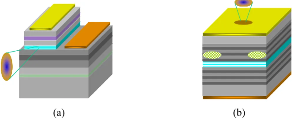
Fig. 5.1 (a) The schematic diagram of conventional GaN based MCLED. (b) The emission image from top view...47
Fig. 5.2 The TRIM profiles of the total number of vacancies produced in GaN by 40 keV C, 100 keV Au, and 300 keV Au ions...48
Fig. 5.3 The interface of the TRIM simulation software...49
Fig. 5.4 (a) Depth profiles of the distribution of the damage created in p-GaN during the implantation process with 80 keV Mg ions. (b) TRIM simulation under the same condition...50
Fig. 5.5 The SIMS profiles and the corresponding TRIM simulation of the damage created in MCLED structures using 50nm/100nm thick SiNx buffer layer during the implantation process of 80keV Mg ions with a does of 2E15...51
Fig. 5.6 The 2D schematic diagram of nitride structure of MCLED grown by MOCVD...53
Fig. 5.7 1st step of process: mesa...54
Fig. 5.8 2nd step of process: buffer layer...54
Fig. 5.9 3rd step of process: blocking metal...54
Fig. 5.10 4th step of process: Implant...54
Fig. 5.11 Remove Au metal and SiNx film...54
Fig. 5.12 5th step of process: TCL...54
Fig. 5.13 6th step of process: N-contact...55
Fig. 5.14 7th step of process: P-contact...55
Fig. 5.15 Probe station measurement instrument setup...56
Fig. 5.16 Emission images of Mg implanted MCLED with six aperture size...57
Fig. 5.17 The emission images and structures of Mg implanted and conventional MCLEDs. (a) Conventional MCLED. (b) Implanted MCLED...57
Fig. 5.18 (a) The emission images of Mg+ implanted MCLED after deposition of ITO transparent contact layer. (b) The emission image of aperture size of 40μm under high magnification. (c) The structure of implanted MCLED after deposition of ITO transparent contact layer...58
Chapter1
Overview
1.1 Introduction
GaN-based materials have been attracting a great deal of attention in the early 1990s due to the large direct band gap and the promising potential for the optoelectronic devices, including light emitting diodes (LEDs) and laser diodes (LDs) [1-7]. In 1993 the first prototype high brightness ( > 100 times greater than previous alternatives, about 1 candela) GaN-based blue LEDs were developed by Nakamura’s group, also they developed the first GaN-based violet LD with an emission wavelength of around 400nm in 1996[5]. From that time, research groups in the laboratories and companies have spent more time on the development of GaN-based devices and many commercial products with various applications were produced. Today, blue LEDs are widely used in many applications such as illumination, exterior automotive lighting, full color display, traffic signals, back light of liquid crystal display and etc. The blue LD can serve as the light source of high density data storage (about 25GB/disk, 5 times larger than now) in high definition digital versatile disk (HD-DVD) which is the main stream of next generation data storage. The big market of HD-DVD has shown up the importance of blue LDs. Besides, the blue and violet LDs may have many other possible markets, such as high brightness projector, high speed printer, medical field and others. However, commercial blue LDs are edge emitting lasers (EELs), not vertical cavity surface emitting lasers (VCSELs). The VCSEL possesses many advantageous properties over the EEL, including circular beam shape, light emission in vertical direction, low cost and formation of two-dimension arrays. In particular, the use of two-dimensional arrays of the blue VCSEL could reduce the read-out time in high density optical storage and increase the scan speed in high-resolution laser printing technique. Recently, many efforts were devoted to the fabrication of GaN-based VCSEL, and some optically pumped laser operation results were achieved and reported [8-14]. Although electrically injected GaN-based VCSEL has not to date been achieved, some VCSEL-like GaN-based microcavity light emitting diodes (MCLEDs)
[15-22], the basis of electrically injected GaN-based VCSEL, have also been reported. In brief,
the GaN-based MCLED is an electronic surface emitting device with VCSEL structure but unable to achieve the stimulated emission yet. However, it is believed that the obtainment of high quality materials, performed by the improvement of the epitaxially grown technique of VCSEL structure, would realize the electrically injected GaN-based VCSEL.
1.2 GaN-based Surface Emitting Devices
The fabrication of GaN-based surface emitting devices, including GaN-based VCSEL and MCLED, requires a pair of high-reflectivity mirrors, usually in the form of DBRs, for forming a high quality vertical cavity. The favorite design of GaN-based surface emitting device is the hybrid structure employed the in-situ epitaxially grown nitride-based DBR, and the dielectric DBR. Compared to the structure with all epitaxially grown DBRs or all dielectric DBRs, the hybrid one is more easy and convenient. In addition, most reported GaN-based surface emitting devices employed more than 40 pairs AlxGa1-xN/GaN DBR to form the high reflectivity mirror [8][11][19]. However, the high refractive index contrast between AlN/GaN indicates that about 20~25 pairs AlN/GaN DBR could achieve high reflectivity and also suggests that using AlN/GaN DBRs as the reflecting mirror of GaN-based surface emitting device could be the better choice. But, the AlN/GaN combination has relatively large lattice mismatch (~2.4%) that tends to cause cracks in the epitaxial film during the growth of the AlN/GaN DBR structure and could result in the reduction of reflectivity and increase in scattering loss. Therefore, GaN-based VCSELs and MCLEDs employed AlN/GaN DBRs were not reported until now. Recently, we have achieved high-reflectivity AlN/GaN DBR structure with relatively smooth surface morphology and could be used in the GaN-based surface emitting device [23][24].
1.3 Objective of the Thesis
In this thesis, we report two fabrication techniques for GaN based micro-cavity light emitting diode (MCLED), an initial step toward electrically injected VCSEL. One is the substitution of the Ni/Au transparent contact layer by ITO. We present the electrical and optical characteristics of the device – including I-V curve, L-I curve, and the EL spectrum. Another technique is using the Mg ion implantation for current confinement in GaN based MCLED. The process flowchart and electrical and optical characteristics of GaN based MCLED are also presented. Such techniques could be the basis for electrically injected GaN-based VCSEL.
1.4 Outline of the Thesis
This thesis is organized in the following manner. In chapter 2 and chapter 3 , the formation, operation mechanism and applications of VCSEL and the fundamentals of ion implantation are briefly introduced. In chapter 4, the characteristics of MCLED using ITO as transparent contact layer are presented and compared with the MCLED using Ni/Au as transparent contact layer. In chapter 5, we describe the fabrication and characteristics of GaN-based MCLED using Mg ion implantation for current confinement. Finally, chapter 6 is the conclusion.
Chapter2
Fundamentals of VCSEL and Febry-Perot Resonator
2.1 Introduction to VCSELs
[25-27]What is VCSEL? It is a contracted name of vertical cavity surface emitting laser and it is a kind of semiconductor laser. What’s the advantage of VCSEL? What’s the application of VCSEL? Before talking about these, let’s review the history of the semiconductor laser.
History overview
More than forty years have been passed since the solid-state ruby laser and the He-Ne gas laser were successfully made in 1960. It was from that time, more efforts have been put on the research of laser, especially the possibility of lasing in semiconductor laser. In 1962, first stimulated emission in semiconductor laser was reported by several groups. Then, the research of the semiconductor laser never stop until now, and the related products, such as optical disc players, laser printers, and fiber communication links, have played an important role in our daily life. However, the conventional used semiconductor laser, edge emitting laser (EEL), as shown in Fig 2.1(a), still has some problems, e.g. , the initial probe test of such devices is impossible before separating into chips, the monolithic integration of lasers into an optical circuit is limited due to the finite cavity length, and so on. In 1977, K. Iga at the Tokyo Institute of Technology, Tokyo, Japan suggested a vertical cavity surface emitting laser for the purpose of overcoming such difficulties as mentioned above [28]. As the name suggests, VCSEL emission occurs perpendicular, rather than parallel, to the wafer surface. The cavity is formed by two surfaces of an epitaxial layer, and light output is taken vertical from one of the mirror surfaces, as depicted in Fig 2.1(b). According to the suggested laser structure, many novel advantages could be done if VCSEL is realized.
(a) (b)
Figure 2.1 Schematic diagrams of (a) an EEL and (b) a VCSEL.
The advantages of VCSEL stated by Iga are as follows [28]. (1) The laser device is fabricated by a fully monolithic process. (2) A densely packed two-dimensional laser array could be fabricated. (3) The initial probe test could be performed before separation into chips. (4) Dynamic single longitudinal mode operation is expected because of its large mode spacing. (5) It is possible to vertically stack multithin-film functional optical devices on to the VCSEL. (6) A narrow circuit beam is achievable. These benefits of VCSEL encourage the researchers to devote themselves to speeding up the development of VCSEL. In 1979, Iga demonstrated first VCSEL used 1.3µm-wavelength GaInAsP/InP material for the active region. In 1984, they made a room temperature pulsed operation GaAs-based device, and the first room temperature continuous wave (CW) operation GaAs-based VCSEL was fabricated in 1987. Until now, Iga has done a lot of research and improvement on VCSEL. It is worth to say, his outstanding contributions on VCSEL earn him the name of “Father of VCSEL”. So far, GaAs-based device have been extensively studied and some of the 0.98, 0.85, and 0.78µm wavelength devices are now commercialized into optical systems. Besides, the technique of 1.3 and 1.5µm devices has already set up. In the mean while, green-blue-ultraviolet device research has been started. It is believed that the commercial products with green-blur-ultraviolet VCSEL will come out in no more future.
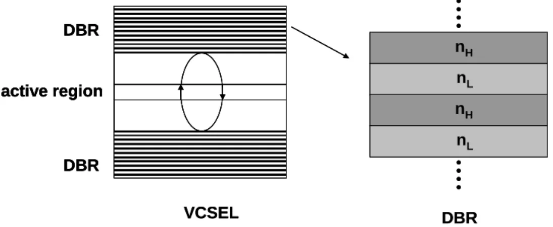
Typical structure of VCSEL
Typical structure of VCSEL includes central active region and the top and bottom high reflecting mirror, as shown in Fig 2.2. Besides, the high reflecting mirror is usually in the form of distributed Bragg reflectors (DBRs), composed of high and low reflection index material quarter wavelength stack, as shown in Fig 2.2. The light is amplified in the microcavity and emission out in the vertical direction. The entirely operation mechanism of VCSEL will be discussed later in section 2.5, and the theory of DBRs will also be reported in section 2.2. active region DBR DBR nH nL nH nL VCSEL DBR active region DBR DBR active region DBR DBR nH nL nH nL VCSEL DBR
Advantages of VCSEL
In the past, the semiconductor laser market was filled with the product which applied the EEL, especially in optical storage devices (780nm lasers for CDs and 650nm lasers for DVDs). Recent, the semiconductor laser market has been shared by the VCSEL, due to the demand of the optical data link. Besides, the development of VCSEL grew up vary quickly these years, and more advantages of VCSEL start to surface. These advantages are as follows.
Technical advantages:
(1) Vertical emission from the substrate with circular beam is easy to couple to optical fibers. (2) Low threshold and high driving current operation is possible.
(3) Large relaxation frequency provides high speed modulation capability.
(4) Single mode operation is possible, and wavelength and threshold are relatively insensitive against temperature variation
(5) Long device lifetime and high power-conversion efficiency.
Manufacturing and cost advantages:
(1) Smaller size of laser devices can lower the cost of the wafer.
(2) The initial probe test can be performed before separating devices into discrete chips. (3) Easy bonding and mounting, cheap module and package cost.
(4) Densely packed and precisely arranged two-dimensional laser arrays can be performed. (5) It is possible to vertically stack multithin-film functional optical devices on to the VCSEL.
Applications of VCSEL
The application of VCSEL is mainly on optical data transmission, including optical interconnects, parallel data links, and so on. The 1300nm and 1550nm long wavelength VCSEL should be useful for silica-based fiber links, providing ultimate transmission capability by taking advantage of single wavelength operation and massively parallel integration. The 650nm VCSEL is useful for short-distance data links by using 1mm diameter low loss plastic fibers. Moreover, blue to UV VCSEL should be useful in the high density data storage. Now, more and more applications of VCSEL are under development, such as compact disc optical pickup modules, printing heads, optical scanners, optical displays, projection systems, and optical sensor. It is believed that those products will be made sooner or later.
2.2 The Theory of DBRs
The DBRs are a simplest kind of periodic structure, which is made up of a number of quarter-wave layers with alternately high- and low- index materials. Therefore, it’s necessary to know the theory of quarter-wave layer before discussing the DBRs.
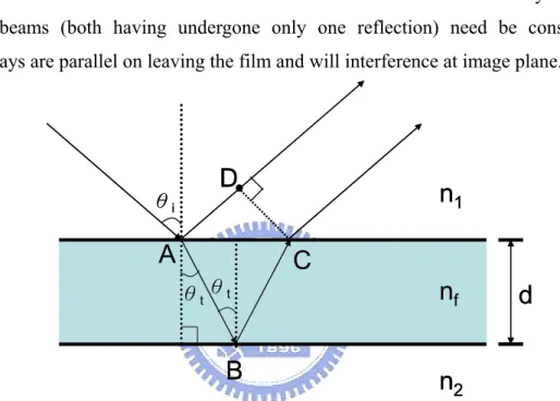
Quarter-wave layer [29-30]
Consider the simple case of a transparent plate of dielectric material having a thickness d and refractive index nf, as shown in Fig 2.3. Suppose that the film is nonabsorbing and that the amplitude-reflection coefficients at the interfaces are so low that only the first two reflected beams (both having undergone only one reflection) need be considered. The reflected rays are parallel on leaving the film and will interference at image plane.
d
A
B
C
D
θi θtθtn
fn
1n
2d
A
B
C
D
θi θtθtn
fn
1n
2Figure 2.3 Schematic draw of the light reflected from the top and bottom of the thin film. The optical path difference (P) for the first two reflected beam is given by
(2.1) ) ( )] ( ) [(AB BC n1 AD n P= f + − and since (2.2) t d BC AB) ( ) cosθ ( = = ) ( cos 2 1 AD n d n P t f − = θ (2.3) (2.4) also (AD)=(AC)sinθi t i f n n AC AD) ( ) sinθ ( = (2.5)
Using Snell’s Law
(2.6)
t
d
AC) 2 tanθ
) sin 1 ( cos 2 2 t t d n P f θ θ − =
The expression for P now becomes (2.7)
(2.8)
or finally P=2 dnf cosθ
The corresponding phase difference (δ) associated with the optical path length difference is then just the product of the free-space propagation number and P, that is, KoP. If the film is immersed in a single medium, the index of refraction can simply be written as n1=n2=n. It is noted that no matter nf is greater or smaller than n, there will be a relative phase shift π radians. (2.9) 4 ) 1 2 ( cos t m f d θ = + λ Therefore, π θ λ π δ = 2− 2 2 2± 0 ( sin ) 4 i n n n f f (2.10) or
The interference maximum of reflected light is established when δ=2mπ, in other words, an even multiple of π. In that case Eq. (2.9) can be rearranged to yield
[maxima] (m = 0, 1, 2,…) (2.11) f n m d t 4 ) 1 2 ( cosθ = + λ0
The interference maximum of reflected light is established when δ=(2m±1)π, in other words, an odd multiple of π. In that case Eq. (2.9) can be rearranged to yield
[minima] (m = 0, 1, 2,…) (2.12) f n m d t 4 2 cosθ = λ0
Therefore, for an normal incident light into thin film, the interference maximum of reflected light is established when d = λ0/4nf (at m=0). Based on the theory, a periodic structure of
alternately high- and low- index quarter-wave layer is useful to be a good reflecting mirror. This periodic structure is also called Distributed Bragg Reflectors (DBRs).
Distributed Bragg Reflectors (DBRs) [25-26][31-34]
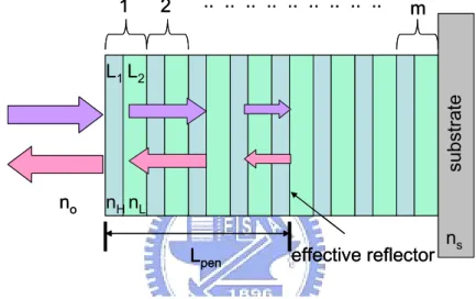
DBRs serve as high reflecting mirror in numerous optoelectronic and photonic devices such as VCSEL. There are many methods to analyze and design DBRs, and the matrix method is one of the popular one. The calculations of DBRs are entirely described in many optics books, and the derivation is a little too long to write in this thesis. Hence, we put it in simple to understand DBRs. Consider a distributed Bragg reflector consisting of m pairs of two dielectric, lossless materials with high- and low- refractive index nH and nL, as shown in Fig 2.4. The thickness of the two layers is assumed to be a quarter wave, that is, L1 =λB/4nH and L2 =λB/4nL, where theλB is the Bragg wavelength.
Multiple reflections at the interface of the DBR and constructive interference of the multiple reflected waves increase the reflectivity with increasing number of pairs. The reflectivity has a maximum at the Bragg wavelength λB. The reflectivity of a DBR with m quarter wave pairs at the Bragg wavelength is given by
L1L2 nHnL 1 2 .. .. .. .. .. .. .. .. .. m effective reflector Lpen ns su bs tra te no L1L2 nHnL 1 2 .. .. .. .. .. .. .. .. .. m effective reflector Lpen ns su bs tra te no
Figure 2.4 Schematic diagram of DBRs.
⎟⎟ ⎟ ⎟ ⎠ ⎞ ⎜⎜ ⎜ ⎜ ⎝ ⎛ + − = p p H L o s H L o s n n n n n n n n R 2 2 ) ( 1 ) ( 1 (2.13)
where the no and ns are the refractive index of incident medium and substrate.
The high-reflectivity or stop band of a DBR depends on the difference in refractive index of the two constituent materials, △n (nH-nL). The spectral width of the stop band is given by
eff B stopband n n π λ λ = Δ Δ 2 (2.14)
where neff is the effective refractive index of the mirror. It can be calculated by requiring the same optical path length normal to the layers for the DBR and the effective medium. The effective refractive index is then given by
1 ) 1 1 ( 2 + − = L H n n neff
The length of a cavity consisting of two metal mirrors is the physical distance between the two mirrors. For DBRs, the optical wave penetrates into the reflector by one or several quarter-wave pairs. Only a finite number out of the total number of quarter-wave pairs are effective in reflecting the optical wave. The effective number of pairs seen by the wave electric field is given by
(2.15) (2.16) ) 2 tanh( 2 1 L H L H L H L H n n n n m n n n n meff + − − + ≈
For very thick DBRs (m→∞) the tanh function approaches unity and one obtains
L H L H n n n n meff − + ≈ 2 1 (2.17) (2.18) Also, the penetration depth is given by
) 2 tanh( 4 2 1 mr r L L Lpen= +
where r = (n1-n2)/ (n1+n2) is the amplitude reflection coefficient.
For a large number of pairs (m→∞), the penetration depth is given by
L H L H n n n n L L r L L Lpen − + + = + ≈ 4 4 2 1 2 1 (2.19) (2.20) Comparison of Eqs. (2.17) and (2.19) yields that
) ( 2 1 2 1 L L m Lpen= eff +
The factor of (1/2) in Eq. (2.20) is due to the fact that meff applies to effective number of periods seen by the electric field whereas Lpen applies to the optical power. The optical
power is equal to the square of the electric field and hence it penetrates half as far into the mirror. The effective length of a cavity consisting of two DBRs is thus given by the sum of the thickness of the center region plus the two penetration depths into the DBRs.
2.3 Febry-Perot Resonator
[25-26][31-34]Background
The Fabry-Perot interferometer was first built and analyzed by the French physicists Fabry and Perot at the University of Marseilles about one century ago and made use of interference of light reflected many times between two coplanar lightly-silvered mirrors. It is a high resolution instrument that has been used today in precision measurement and wavelength comparisons in spectroscopy. Recent, it has come into prominence as the Fabry-Perot cavity employed in nearly all lasers. The Fabry-Perot cavities can be used to ensure precise tuning of laser frequencies.
Theory
A schematic draw of a Fabry-Perot cavity with two metallic reflectors with reflectivity R1 and R2 is shown in Fig 2.5. Plane waves propagating inside the cavity can interference constructively and destructively resulting in stable (allowed) and attenuated (disallowed) optical modes, respectively. The allowed frequencies are integer multiples of the mode spacing △ν = c/2nLc, where Lc is the length of the cavity, c is the velocity of light in vacuum.
Figure 2.5 A schematic draw of a Fabry-Perot cavity with two metallic reflectors with reflectivity R1 and R2
For lossless reflectors, the transmittance through the two reflectors is given by T1 = 1-R1, and T2 = 1-R2. Taking into account multiple reflections inside the cavity, the transmittance through a Fabry-Perot cavity can be expressed in terms of a geometric series. The transmitted light intensity (transmittance) is then given by
φ 2 cos 2 1 1 2 1 2 2 1 R R R R T T T − + =
where ψ is the phase change of the optical wave for a single pass between the two reflectors. The ψ can also be expressed in term of wavelength and frequency by using
(2.21) (2.22) c nL nLc π cυ λ π φ =2 =2
The maxima of the transmittance occur if the condition of constructive interference is fulfilled, that is, if ψ= 0, 2π,...,. Insertion of these values into Eq. (2.21) yields the transmittance maxima as 2 2 1 2 1 max ) 1 ( RR T T T + = (2.23)
For asymmetric cavities (R1≠R2), it is Tmax < 1. For symmetric cavities (R1 = R2), the transmittance maxima are unity, Tmax = 1. Near ψ= 0, 2π,..., the cosine term in Eq. (2.21) can be expanded into a power series (cos2ψ~1- 2ψ2
). One obtains 2 2 1 2 2 1 2 1 4 ) 1 ( R R RR ϕ T T T + = −
Equation (2.24) indicates that near the maxima, the transmittance can be approximated by a Lorentzian function. The transmittance T in Eq. (2.24) has a maximum at ψ= 0. The
transmittance decreases to half of the maximum value at 1/2
2 1 2 1 )/(4 ) 1 ( 2 / 1 = − RR R R φ . For
high values of R1 and R2 (i.e., R1~1 and R2~1), it is φ1/2=(1/2)(1− R1R2).
2.4 The Finesse and the Quality Factor of Resonant Cavity
[25-26][31-34]Since the theory of Fabry-Perot cavity has been explained, we can talk about the finesse and the quality factor of resonant cavity. The cavity finesse, F, is defined as the ratio of the transmittance peak seperation (△ψ) to the transmittance full-width at half-maximum (δψ):
(2.24) (2.25) 2 1 2 / 1 1 2 RR F − = = Δ = π φ π δφ φ
Figure 2.6 shows the transmission pattern of a Fabry-Perot cavity in frequency domain. The finesse of the cavity in the frequency is then given by F = νFSR/△ν.
ν0 2ν0 3ν0 In te ns ity ν0 2ν0 3ν0 In te ns ity
Figure 2.6 The transmission pattern of a Fabry-Perot cavity in frequency domain.
The cavity quality factor Q is frequently used and is defined as the ratio of the transmittance peak frequency (ψ) to the peak width (δψ):
2 1 1 2 R R nL Q c − = = π λ δφ φ (2.26) Besides the quality factor Q is also equal to λ/δλ, where δλ is the narrow emission linewidth around λ. (2.27) δλ λ = Q
2.5 Operation Mechanism of VCSEL
[25-27][35-38]The operation of a VCSEL, like any other diode lasers, can be understood by observing the flow of carriers into its active region, the generation of photons due to the recombination of some of these carriers, and the transmission of some of these photons out of the optical cavity. These dynamics can be described by a set of rate equations, one for the carriers and one for the photons in each of the optical modes. In fact, the construction of such rate equations provides a clear definition of the basic laser parameters that we will need in describing the terminal characteristic of the VCSEL.
Carrier density rate equation
The carrier density in the active region is governed by a dynamic process. In fact, we can compare the process of establishing a certain steady-state carrier density in the active region to that of establishing a certain water level in a reservoir which is being simultaneously filled and drained. This is shown schematically in Fig. 2.7. As we proceed, the various filling (generation) and drain (recombination) terms illustrated will be defined. The current leakage illustrated in Fig. 2.7 contributes to reducing ηi and is created by possible shunt paths around the active region. The carrier leakage, Rl, is due to carriers “splashing” out of the active region (by thermionic emission or lateral diffusion if no lateral confinement exists) before recombining. Thus, this leakage contributes to a loss of carriers in the active region that could otherwise be used to generate light.
Rnr Rl Rsp~ BN2 Rst~ gvgNp current leakage Nth I / qV Ggen= ηiI / qV Rnr+ Rl~ (AN+CN3) electron photon Rrec= Rsp+ Rnr+ Rl+ Rst rec gen R G dt dN = − rate equation : Rnr Rl Rsp~ BN2 Rst~ gvgNp current leakage Nth I / qV Ggen= ηiI / qV Rnr+ Rl~ (AN+CN3) electron photon Rrec= Rsp+ Rnr+ Rl+ Rst rec gen R G dt dN = −
rate equation : dt Ggen Rrec
dN = −
rate equation :
Figure 2.7 Reservoir with continuous supply and leakage as an analog to a DH active region with current injection for carrier generation and radiative and nonradiative recombination.
For the DH active region, the injected current provides a generation term, and various radiative and nonradiative recombination process as well as carrier leakage provide recombination terms. Thus, we can write the carrier density rate equation,
(2.28) rec gen R G dt dN − =
where N is the carrier density (electron density), Ggen is the rate of injected electrons and Rrec is the ratio of recombining electrons per init volume in the active region. Since there areηi I/q electrons per second being injected into the active region,
qV I
G i
gen
η
= , where V is the volume
of the active region. The recombination process is complicated and several mechanisms must
be considered. Such as, spontaneous recombination rate, Rsp ~ BN2, nonradiative
recombination rate, Rnr, carrier leakage rate, Rl, (Rnr + Rl = AN+CN3), and stimulated recombination rate, Rst. Thus we can write Rrec = Rsp + Rnr + Rl +Rst. Besides, N/τ ≡ Rsp + Rnr + Rl, where τ is the carrier lifetime. Therefore, the carrier density rate equation could be expressed as carrier density rate equation st i N R qV I dt dN = − − τ η (2.29)
Photon density rate equation
Now, we describe a rate equation for the photon density, Np, which includes the photon
generation and loss terms. The photon generation process includes spontaneous recombination (Rsp) and stimulated recombination (Rst), and the main photon generation term of laser above threshold is Rst. Every time an electron-hole pairs is stimulated to recombine, another photon is generated. Since, the cavity volume occupied by photons, Vp, is usually larger than the active region volume occupied by electrons, V, the photon density generation rate will be [V/Vp]Rst not just Rst. This electron-photon overlap factor, V/Vp, is generally referred to as the
confinement factor, Γ. Sometimes it is convenient to introduce an effective thickness (deff),
width (weff), and length (Leff) that contains the photons. That is, Vp=deffweffLeff. Then, if the active region has dimensions, d, w, and La, the confinement factor can be expressed as, Γ=ΓxΓyΓz, whereΓx = d/deff, Γy = w/weff, Γz = La/Leff. Photon loss occurs within the cavity due to optical absorption and scatting out of the mode, and it also occurs at the output coupling mirror where a portion of the resonant mode is usually couple to some output medium. These net losses can be characterized by a photon (or cavity) lifetime, τp. Hence, the photon density rate equation takes the form
photon density rate equation p p sp sp st p R R N dt dN τ β − Γ + Γ = (2.30)
where βsp is the spontaneous emission factor. As to Rst, it represents the photon-stimulated net electron-hole recombination which generates more photons. This is a gain process for
photons. It is given by p g p st gen p v N t N R dt dN g = Δ Δ = = ⎟⎟ ⎠ ⎞ ⎜⎜ ⎝ ⎛ (2.30) where vg is the group velocity and g is the gain per unit length.
Now, we rewrite the carrier and photon density rate equations carrier density rate equation g p i N v N qV I dt dN g − − = τ η (2.31) photon density rate equation p p sp sp p g p N R N v dt dN τ β − Γ + Γ = g (2.32) Threshold gain
In order for a mode of the laser to reach threshold, the gain in the active section must be increased to the point when all the propagation and mirror losses are compensated. As illustrated in Fig. 2.8, most laser cavities can be divided into two general sections: an active section of length La and a passive section of length Lp. The threshold gain is given by
⎟⎟ ⎠ ⎞ ⎜⎜ ⎝ ⎛ + = Γ 2 1 1 ln 2 1 R R L i α th g
where αi is the average internal loss which is defined by (αiaLa + αipLp)/L, and R1 and R2 is the reflectivity of top and bottom mirror of the laser cavity, respectively. For convenience the mirror loss term is sometimes abbreviated as, αm ≡ (1/2L) ln(1/R1R2). Noting that the cavity
life time (photon decay rate) is given by the optical loss in the cavity, 1/τp = 1/τi + 1/τm =
vg(αi +αm). Thus, the threshold gain in the steady state can be expressed with following
equation (2.33) (2.34) ⎟⎟ ⎠ ⎞ ⎜⎜ ⎝ ⎛ + = = + = Γ 2 1 1 ln 2 1 1 R R L vg p i m i α τ α α th g
La Leff L=La+Lp La Leff L=La+Lp
Figure 2.8 Schematic diagram of VCSEL
Output power versus driving current
The characteristic of output power versus driving current (L-I characteristic) in a laser diode can be realized by using the rate equation Eq. (2.31) and (2.32). Consider the below threshold (almost threshold) steady-state (dN/dt = 0) carrier rate equation, the Eq. (2.31) is
given by
(
)
τ η th th l nr sp th i R R R N qV I = + += . While the driving current is above the threshold
(I>Ith), the carrier rate equation will be
above threshold carrier density rate equation (2.35) p g th i v N qV I I dt dN g − − =η ( )
From Eq. (2.35), the steady-state photon density above threshold where g = gth can be calculated as steady state photon density qv V I I N th g th i p g ) ( − =η (2.36)
The optical energy stored in the cavity, Eos, is constructed by multiplying the photon density, Np, by the energy per photon, hν, and the cavity volume, Vp. That is Eos = NphνVp. Then, we
multiple this by the energy loss rate through the mirrors, vgαm = 1/τm, to get the optical power output from the mirrors, P0 = vgαmNphνVp. By using Eq. (2.34) and (2.36), and Γ=V/Vp, we can write the output power as the following equation
) ( th m i m i O I I q h P ⎟⎟ − ⎠ ⎞ ⎜⎜ ⎝ ⎛ + = ν α α α η (2.37) output power Now, by defining m i m i d αα α η
η = , the Eq. (2.37) can be simplified as ) ( th d O I I q h P =η ν − (I > Ith) (2.38)
Thus, the ηd can be expressed as
dI dP h q O d ⎥⎦ ⎤ ⎢⎣ ⎡ = ν η (I > Ith) (2.39)
differential quantum efficiency
In fact, ηd is the differential quantum efficiency, defined as number of photons out per electron. Besides, dPo/dI is defined as the slope efficiency, Sd, equal to the ratio of output power and injection current. Figure 2.9 shows the illustration of output power vs. current for a diode laser. below threshold only spontaneous emission is important; above threshold the stimulated emission power increase linearly with the injection current, while the spontaneous emission is clamped at its threshold value.
I
thI
P
o ⎟⎟ ⎠ ⎞ ⎜⎜ ⎝ ⎛ + = 2 1 1 ln 2 1 R R L i th α g spontaneous emissionsection laser oscillation section
spontaneous emission q I h Po d / / Δ Δ = ν η I P S o d Δ Δ = P Δ I Δ
I
thI
P
o ⎟⎟ ⎠ ⎞ ⎜⎜ ⎝ ⎛ + = 2 1 1 ln 2 1 R R L i th α g spontaneous emissionsection laser oscillation section
spontaneous emission q I h Po d / / Δ Δ = ν η I P S o d Δ Δ = P Δ I Δ
2.6 Work Review
Optically pumped VCSEL[39]
In our previous work, the characteristics of a GaN-based VCSEL with 25 pairs AlN/GaN DBR (with reflectivity about 95%) and 8 pairs Ta2O5/SiO2 DBR (with reflectivity about 97.5%) was successfully fabricated and investigated. The schematic diagram and SEM image of the overall VCSEL structure are shown in the Fig 2.10 (a) and (b). A narrow PL emission with full width at half maximum of 1.4nm corresponds to the cavity resonant mode at 448nm was observed, as shown in Figure 2.11. The cavity quality factor, estimated from the emission linewidth of 1.4nm, was about 320. Figure 2.12 shows the laser action was achieved under the optical pumping at room temperature with a threshold pumping energy density of about 53mJ/cm2. The GaN VCSEL emits 448nm blue wavelength with a linewidth of 0.17nm. The estimation of the carrier density and gain at the threshold were about 3×1020 cm-3 and 1.45×104 cm-1, respectively. The NFP and FFP showed that the beam width and divergence angle were about 3.0µm and 7.6o, respectively. The NFP and FFP also indicated that the shape of laser emission was close to a circle. The laser beam showed a degree of polarization of about 84% suggesting strong polarization property of the laser emission. The characteristic temperature of fabricated VCSEL was about 243K suggesting good temperature tolerance.
10 pairs of In0.2Ga0.8N/GaN MQW 25 pairs of AlN/GaN DBR 2μm GaN Sapphire n-GaN p-GaN 8 pairs of Ta2O5/SiO2DBR 10 pairs of In0.2Ga0.8N/GaN MQW 25 pairs of AlN/GaN DBR 2μm GaN Sapphire n-GaN p-GaN 10 pairs of In0.2Ga0.8N/GaN MQW 25 pairs of AlN/GaN DBR 2μm GaN Sapphire n-GaN p-GaN 8 pairs of Ta2O5/SiO2DBR Ta2O5/SiO2 DBR AlN/GaN DBR 3-λ Cavity Ta2O5/SiO2 DBR AlN/GaN DBR 3-λ Cavity (a) (b)
Figure 2.10 (a) The schematic diagram of the overall VCSEL structure (b) The SEM image of the overall VCSEL.
425 430 435 440 445 450 455 460 465
448nm
1.4nm
Wavelength (nm)
Figure 2.11 PL emission of the overall VCSEL structure.
0.0 0.5 1.0 1.5 2.0 2.5 3.0 3.5 0 5000 10000 15000 20000 25000 E m is s io n in te n s ity (a .u .)
Excitation energy (μJ/pulse)
430 440 450 460 470 480 1.71Eth 1.43Eth 1.14Eth 0.86Eth 1.00Eth E m is s io n i n te n s ity (a .u .) Wavelength (nm) 0.0 0.5 1.0 1.5 2.0 2.5 3.0 3.5 0 5000 10000 15000 20000 25000 E m is s io n in te n s ity (a .u .)
Excitation energy (μJ/pulse)
430 440 450 460 470 480 1.71Eth 1.43Eth 1.14Eth 0.86Eth 1.00Eth E m is s io n i n te n s ity (a .u .) Wavelength (nm)
GaN based Micro-cavity light emitting diode (MCLED)
With the achievement of optically pumped GaN-based VCSEL, the realization of electrically-injected GaN-based VCSEL has become promising. So far, the electrically injected GaN based VCSEL has not been realized. However, the micro-cavity light emitting diodes (MCLEDs) [15-22], with a quasi VCSEL structure, could be served as an initial step toward electrically injected GaN VCSEL. They mainly utilized an epitaxially growth nitride DBR as the bottom mirror and a dielectric DBR as the top mirror. This kind of device has several advantages comparable to VCSEL, such as circular beam shape, light emission in vertical direction, fully monolithic test and two dimensional arrays. Some GaN-based MCLEDs with an in-situ epitaxially grown nitride-based DBRs and dielectric DBRs as the bottom and upper mirror of the cavity were reported. Recently, Diagne et al. [15] employed 60 pairs of GaN/Al0.25Ga0.75N DBR as bottom mirror (with reflectivity of 99%) and SiO2/HfO2 as top mirror (with reflectivity of 99.5%). The schematic diagram and EL spectrum of this MCLED are both shown in Figure 2.13. The emission peak wavelength of the MCLED was located at 413nm with a narrow line width of 0.6nm. It means the Q factor is about 690. This result was the best value compared with the Q factor of the MCLED published in the recent literature.
Chapter3
Fundamentals of Ion Implantation
3.1 Introduction to Ion Implantation
[40-43]3.1.1 Introduction
For much of the past decade, GaN has been a subject of extensive research due to very important technological applications of this material. As is well documented in the literature, current applications of GaN include light-emitting diodes (LEDs), laser diodes, UV detectors, and microwave power and ultra-high power switches. In the fabrication of such GaN-based devices, ion implantation represents a very attractive tool for several technological steps, such as electrical and optical selective-area doping, dry etching, electrical isolation, quantum well intermixing, and ion-cut. It is well-known that a successful application of ion implantation depends on understanding the production and annealing of radiation damage. Thus, detailed studies of ion implantation damage in GaN are not only important for investigating
fundamental defect processes in solids under ion bombardment but are also essential for the fast developing GaN industry.
3.1.2 History overview
The beginnings of ion implantation are now more than twenty years in the past. In 1957, Shockley obtained the first patent for the technique of ion implantation. In this patent, it was pointed out for the first time that annealing after implantation is necessary for
re-crystallization of the crystal lattice. This patent covers practically all aspects of
implantation. From then on, more and more articles dealing with implantation were published. The final breakthrough began in the middle of the 1960s. For the production of MOS
transistors, the use of implantation has become generally accepted; hardly any integrated MOS circuit is produced nowadays without the use of one or more implantation steps. In the field of bipolar transistors. The use of implantation is steadily increasing, while it is already being employed as standard technology for several special devices.
Implantation offers a number of technological advantages which are important in the fabrication of optoelectronic devices:
1. Speed, homogeneity, and reproducibility of the doping process. 2. Avoidance of high processing temperatures during implantation.
3. Simple masking methods, for example, with the use of thick layers of oxide, nitride, metal or photoresist.
5. Low penetration depth of the ions; it is possible to dope shallow layers with very high doping gradients.
6. Multiple implantation by changing the accelerator voltage during implantation makes possible a relatively free choice of the doping profile, whereby one is not limited to the Gaussian shape.
7. Because if the minimal lateral scattering, it is possible to fabricate devices with very small dimensions and to keep the parasitic capacitance low.
3.1 Principle of Ion Implantation
Theory of ion stopping
Damage is caused by the ion stopping process in semiconductors. The two important effects in determining the stopping of implanted ion are in the following.
Inelastic collisions of the ions with bound electrons in the crystal. The energy loss in this case is by excitation or ionization of the target atoms. This is termed electronic stopping, and does not create atomic displacements in the material.
Elastic nuclear collisions with nuclei or whole atoms of the crystal, in which a part of the kinetic energy of the incoming ion is transferred to the nuclei that absorb the impact, termed nuclear stopping, and it leads to the creation of deep-level, compensating defects.
The nuclear stopping process of the ion can be considered as caused by collisions between two hard spheres (the ion and the target nuclei) in which the ion loses energy by transferring it to the displaced nuclei. Theoretically this is treated by a Columbic force at a distance
scattering process. One of the important parameters, therefore, is the atomic scattering potential V(r), which is not all that accurately known. The electronic stopping process can be visualized as similar to the stopping of a projectile in a viscous medium with the ion slowed by a series of “drag” interactions.
The relative importance of mechanisms (I) and (II) above depends on the energy and mass of the implanted ions, and the mass and atomic density of the crystal. To calculate stopping of ions, it is useful to introduce the concept of a cross section S for both electronic and nuclear stopping,
n e n e
dx
dE
N
S
,=
−
(
1
)(
)
, (1) Where dx dEis the energy loss per unit distance for either electronic or nuclear stopping, and N is the atomic density of the crystal. The contribution from nuclear energy loss tends to be small at high energies because fast ions have only a short time to interact with a target nucleus,
i.e. they are moving past the target nuclei too fast to efficiently transfer energy to them. At intermediate energies, the nuclear energy loss component increases, but falls again at the lowest energies where electron screening effects lower the ehhective atomic number of the target nuclei.
If both stopping power are independent, then the total energy loss per unit path length of the ion is )] ( ) ( [S E S E N dx dE n e + − = (2) and
∫
∫
=− + = E n e R E S E S dE N dx R 0 0 ( ) ( ) ) 1 ( (3) , where R is the average range or total path length of an ion of energy E in an amorphous crystal, and is proportional to the velocity of the implanted ion, and is proportional to the atomic density of the target and to the total energy transferred in all individual collisions. Knowing and one can obtain the total path length or range, R, of the implanted ion in the target before coming to rest. It is usual to use the projected range , which is defined as the projection of R normal to the surface. For a Gaussian distribution corresponds to the point of maximum concentration of the distribution.) (E Se Sn(E) ) (E Se Sn(E) p R p R
Distribution profile of introduced ions
The range – energy relation given by Eq. (2) was reformulated by Lindhard, Scharff, and Schiott (LSS) for ion implantation into amorphous materials in terms of the reduced parameters, ε, ρ, as: 2 1 ) ( ) ( ε ρ ε ρ ε ε k d d d d n + = (4) Whereρandεare dimensionless variables related to the range, R, and incident energy E0, by:
2 1 2 2 1 4 M M a M RNM + = π ρ (5) and )] ( [ 2 1 2 2 1 2 0 M M q Z Z M Ra + = ε (6)
number of atoms per unit volume; a is the screening length, equal to 3 / 1 2 3 / 1 1 0 88 . 0 Z Z a + , and
is the Bohr radius; and and are the atomic numbers of the ion and target.
0
a
1
Z Z2
The value of ρ was converted to R, and a value for was obtained from approximate expression: p R ) 3 ( 1 1 2 M M R Rp + =
And then the implanted ion concentration, n, as a function of depth, x, can be described as: ] 2 ) ( exp[ 2 ) ( 2 2 p p p R R x R x n Δ − − Δ = π φ
Where Φ is the does (ions/cm2), and
p
R
Δ is the standard deviation of the Gaussian distribution (projected straggle range of the distribution in the direction of incidence of the beam). The value ofΔRpis calculated in terms of and the mass of ions and target atoms, by the approximate expression:
p R ] [ 3 2 2 1 2 1 M M M M R Rp p + = Δ
The LSS assumption is a well simulation of implantation in amorphous materials, but it is not good at single crystal materials due to the channeling effect in the single crystal
materials. In single crystal lattices there are some crystal directions (known as channels) along which the ions will not encounter any target nuclei, and will be channeled along such open channels of the lattice. The channeling effect in single crystal materials can be showed out by the Secondary Ions Mass Spectroscope (SIMS) measurement or the Rutherford
Backscattering Spectroscope (RBS) measurement.
Damage of ion implantation
When the energetic ions strike the GaN target, they lose their energy in a series of nuclear and electronic collisions, and rapidly come to rest some hundreds or some thousands of atom layers below the surface. Only the nuclear collision result in displaced atoms. An individual nuclear collision can different types of displacement events, depending on the magnitude of the energy transferred. If the energy of nuclear collision (△En) transferred to the Ga or N atom is less than the energy required to displace it from its lattice site, Ed, no
displacement event results, if 2Ed>△En>Ed, a single displacement and simple isolated point defects are created. If △En>2Ed, multiple secondary displacements and defect cluster are produced. According to the reports of ion implantation, the single displacement energy of III-V chemical compound is about 20eV. There are about three types of defect made by point defect and cluster defect after ion implantation:
(i) Isolated point defects or point defect clusters in crystalline GaN layer. (ii) Local amorphous layer in an otherwise crystalline GaN layer.
(iii) Continuous amorphous layers in all epitaxial GaN layer.
All the three types of defect need to be annealed out by thermal annealing or another thermal-produced process (RTA) in GaN. The following section is describing the common types of thermal annealing process: rapidly thermal annealing (RTA).
RTA post-annealing
In the semiconductor industry, ion implantation used for electrical and optical doping is always followed by an annealing step. Such annealing is necessary:
(i) To remove implantation-produced lattice disorder.
(ii) To electrically/optically activate implanted species by stimulating their migration into energetically favorable lattice sites.
Post-implantation annealing is a very important technological step since device performance is highly dependent on the efficiency of such annealing.
Isolation
Ion implantation can be employed for two applications in compound semiconductors, namely, the creation of doped regions by implantation and activation of dopant species or the reverse process of creation of high resistance regions by formation of deep traps or
compensating centers. The latter process, named implant isolation, is used for inter-device isolation or to produce current guiding. There is a strong need for an understanding of the implant isolation process in GaN because of the emerging applications for high temperature, high power electronics based on this materials system. Prototype devices such as
hetero-structure field-effect transistors, hetero-junction bipolar transistors, junction field effect transistors, and metal– oxide–semiconductor field-effect transistors have all been
demonstrated, with impressive high temperature (>.300 °C) performance. There are two types of defect-formation mechanisms that are found for implant isolation in semiconductors:
(I) Damage-related isolation: The creation of midgap, damage related levels, which trap
which these damage-related levels are annealed out. For damage compensation, the resistance typically goes through a maximum with increasing post-implantation annealing temperature as damage is annealed out and hopping conduction is reduced. At higher temperatures, the defect density is further reduced below that required to compensate the material, and the resistivity decreases.
(II) Chemically-induced isolation: The creation of chemically induced deep levels by implantation of a species that has an electronic level in the middle of the band gap. This type of compensation usually requires the implanted species to be substitution and hence annealing is required to promote the ion onto a substitutional site. In the absence of out diffusion or precipitation of this species, the compensation is thermally stable. For chemical compensation, the post-implantation resistance again increases with annealing temperature with a reduction in hopping conduction but it then stabilizes at higher temperatures as a thermally stable compensating deep level is formed. Typically, there is a minimum dose (dependent on the doping level of the sample) required for the chemically active isolation species to achieve thermally stable compensation. Thermally stable implant isolation has been reported for n- and p-type AlGaAs where an Al-O complex is thought to form and N in GaAs (C) where C–N complexes are thought to form.
In this study, we use the Mg ion implantation to isolate the GaN for achieving current confinement. The main mechanism to form high resistivity layer is damage induced isolation.
Chapter4
GaN-based Micro-cavity Light Emitting Diodes (MCLEDs) using
ITO as transparent contact layer
4.1 Recent Status
4.1.1 Introduction to Conventional GaN-based MCLED [44]
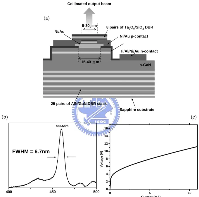
With the achievement of optically pumped GaN-based VCSEL, the realization of electrically-injected GaN-based VCSEL has become promising. So far, we have successfully fabricated the GaN-based MCLED with hybrid structure, composed of high reflectivity, crack-free, wide stop-band width in-situ grown AlN/GaN bottom DBRs (with reflectivity of 95%) and ex-situ deposited SiO2/Ta2O5 top DBRs (with reflectivity of 97.5%). Such device could be used as an initial step toward the GaN-based VCSEL and has several advantages, such as circular beam shape, light emission in vertical direction, fully monolithic test and two dimensional arrays. Figure 4.1 shows the structure and characteristics of the conventional device. The turn on voltage and resistance were about 3.5V and 530Ω, respectively. The device showed the emission wavelength of 458.5nm and FWHM of 6.7nm at 20mA injected current. The previous work was accepted and published by Japanese Journal Applied Physics
letters, Vol. 45, No. 4B, 2006, pp. 3446–3448.
4.1.2 Issue of Q factor
In our previous work, the Q factor of our conventional MCLED could be calculated to be about 68, which is much low than that of our optically pumped VCSEL structure (Q = 320). The main difference between optically pumped VCSEL structure and conventional MCLED structure is the insertion of Ni/Au transparent contact layer. According to laser theory, we can find the Q-factor is inversely proportional to the total loss δ inside the cavity. It suggests that our relatively low Q factor could be attributed to the insertion of Ni/Au transparent contact layer. In order to improve the Q factor of micro-cavity, replacing the Ni/Au transparent
contact layer by another one with high transmittance and low absorption is required. Over few past years, high electrical conductivity and transparency to visible light have made indium tin oxide (ITO) a useful material for transparent contacts to many optoelectronic devices [45]. Rectifying contacts to silicon-, GaAs-, and InP-based solar cells and photo-detectors have already been demonstrated. In the next section, we discuss the effect on Q factor while using
ITO as transparent contact layer for GaN based MCLED, and demonstrate the theoretical calculation to further understand the effect.
Ti/Al/Ni/Au n-contact 8 pairs of Ta2O5/SiO2DBR Ni/Au Ni/Au p-contact 5-30μm 15-40 μm n-GaN
25 pairs of AlN/GaN DBR stack Collimated output beam
Sapphire substrate (a) 0 5 10 0 2 4 6 8 10 12 14 16 Vol tage (V) Current (mA) (c) (b) 400 450 500 458.5nm FWHM = 6.7nm
Figure 4.1 The conventional MCLED using Ni/Au as transparent contact layer.
(a) The structure of conventional MCLED. (b) The EL spectrum of the conventional MCLED. (c) The I-V curve of the conventional MCLED