國立交通大學
電子工程學系電子研究所
博士論文
無摻雜 GaAs/AlGaAs 量子井之橫向 p-i-n 二極體
Lateral p-i-n Diode in an Undoped GaAs/AlGaAs
Quantum Well
研究生 : Dai Van Truong
指導教授 : 李建平 博士
林聖迪 博士
無摻雜 GaAs/AlGaAs 量子井之橫向 p-i-n 二極體
Lateral p-i-n Diode in an Undoped GaAs/AlGaAs
Quantum Well
研究生 : 戴文長 Student: Van-Truong Dai
指導教授 : 李建平 博士 Advisor: Dr. Chien-Ping Lee
林聖迪 博士 Dr. Sheng-Di Lin
國立交通大學
電子工程學系電子研究所
博士論文
A thesis
Submitted to Department of Electronics Engineering and Institute of Electronics
College of Electrical and Computer Engineering National Chiao Tung University
in partial Fulfillment of Requirements for the Degree of Doctor of Philosophy
in
Electronics Engineering
June 2014
Hsinchu, Taiwan, Republic of China 中華民國 一O三年 六月
I
無摻雜 GaAs/AlGaAs 量子井之橫向 p-i-n 二極體
Lateral p-i-n Diode in an Undoped GaAs/AlGaAs
Quantum Well
研究生:戴文長 (Dai Van Truong) 指導教授:李建平 博士
林聖迪 博士
電子工程學系電子研究所
摘要
在表面聲波(SAW)驅動的單光子源元件中,高品質的二維 p-i-n 接面是個關 鍵的因素。另外二維 p-n 橫向接面是另一個在光學方式探討二維系統中電子自旋有 競爭力的選擇。在本論文中,我們發展了一個利用普通的金屬化與曝光製程,可靠 且相對簡單的方式,在完全沒有摻雜的 GaAs/AlGaAs 量子井結構上來製作 p-i-n 橫 向接面。 一個沒有摻雜的異質接面所誘發出的二維電子或電洞氣相較於有摻雜的系 統表現出許多的優點,例如遷移率,特別是在低載子濃度下。為了得到這個優點, 我們發展了一個可被誘發的橫向接面二維 p-i-n 二極體。兩種不同類型的通道透過 金屬-絕緣質-半導體(MIS)閘極,其稱之為單一閘極元件誘發出。在 p 類型施加負電 壓與 n 類型施加正電壓下,2DHG 與 2DEG 通道可以在 GaAs 量子井中被誘發出, 所以一個橫向接面的二維 p-i-n 二極體因此產生。我們研究了這個元件在低溫的電 性與光性。此 2DEG 與 2DHG 被誘發的臨界電壓分別為 3.5V 與 -1.25V。元件的電 壓電流曲線在導通電壓 1.53V 電壓時呈現了清楚的整流特性。及符合理論的計算導 通電壓值 Vbi = 1.535 V。電激發螢光的峰值在 1.529 eV (811 nm)而半高寬有 4.4 meV。這吻合理論計算中量子井基態的能量。II 然而因為閘極與通道的距離使得閘極控制量子井的載子能力並不是非常有 效率。導致兩個在絕緣層上的上層閘極不能彼此靠得太近。這直接影響到在 i 區域 的載子複合。另外這個限制讓元件的發展上更加受限,例如表面聲波驅動的單光子 源。因此我更發展了兩個通道同時有表面閘極與上層閘極的雙閘極結構。這個表面 的蕭基閘極提供了一個通道中載子很好的控制能力下同時可以彼此靠近。跨越源極 與汲極在絕緣層這上的上層閘極,可以在歐姆接觸與閘極間,沒有漏電路徑下控制 著源極與汲極間的通道載子。雙閘極元件表現出較穩定的電性與清楚的光學頻譜。 這些成果展示出這個元件非常適合在單光子元件的應用。
III
Lateral p-i-n Diode in an Undoped GaAs/AlGaAs
Quantum Well
Student: Van-Truong Dai
Advisor: Dr. Chien-Ping Lee
Dr. Sheng-Di Lin
Department of Electronics Engineering & Institute of Electronics
National Chiao Tung University
Abstract
In SAW-driven single-photon source devices, the key component is a high-quality 2-D p-i-n junction. In addition, lateral 2-D p-n junctions are also potential candidates for investigating the properties of electron spins in low-dimensional systems by optical methods. In this thesis, we developed a reliable and relatively easy method to fabricate a lateral p–i–n junction in a completely undoped GaAs/AlGaAs quantum well structure by utilizing conventional metallization and lithography processes.
An induced gas (2DEG or 2DHG) in undoped heterostructure shows great advantages compared to a doped gas, such as high mobility, especially in low carrier density. To gain the advantage of induced gas, we developed an induced lateral 2D p-i-n diode. The two different types of channels are induced via metal-insulator-semiconductor (MIS) gates, which called single-gate devices. With a negative voltage applied on the p-gates and a positive voltage applied on the n-p-gates, both 2DHG and 2DEG channels can be induced in the GaAs quantum well, so a lateral 2-D p-i-n diode is formed. The electrical and optical of the devices at low temperature are studied. The 2DEG and 2DHG can be induced at threshold voltage of 3.5 V and -1.25 V, respectively. The current-voltage curve of the devices shows clearly the rectifying behavior with a turn-on current-voltage of 1.53 V. This is in agreement with the theoretical calculation of the built-in voltage Vbi
IV
= 1.535 V. The main peak of electroluminescence is at 1.529 eV (811 nm) with the full-width at half-maximum of 4.4 meV. This is in good agreement with theoretical calculation of ground state energy of the quantum well.
However, the gate control of the carriers in the quantum well is not very efficient because of the distant gate from the channel. As a result, the two top gates on the insulator could not be put too close to each other. This directly affects the carrier recombination in the i region. In addition, this limits further development more complicated devices, such as SAW-driven single-photon source. Thus, we developed the twin-gate structure which has surface gate and top gate for each channel. The surface Schottky gates provide a very good control for the carriers in the channel and at the same time can be put very close to each other. The top gates, which overlap the source and the drain through the insulator spacer, control the carriers in the channel regions next to the source and the drain without having a leakage path between the gates and the ohmic contacts. The twin-gate devices show more stable electrical characteristics and clearer optical spectrum. These results demonstrate that the device is promising for applications in the single-photon devices.
V
Acknowledgements
I am indebted to many people who contributed in several ways to this thesis, and suppoted me with their cooperation and timely help.
In particular, I would like to acknowledge my adviser, Professor Chien Ping Lee, for providing me an opportunity to work in his research group. He has been a great mentor with his enthusiasm, understanding and willingness to help students professionally and personally. He also has been an exceptional role model of life.
I also would like to thank my co-adviser, Professor Sheng Di Lin, who gave me strong motivation in my research throughout his discussion. I have learnt a lot about methodology of research and life from him. I would like to thank Professor Gray Lin for the many discussions we had about my research, for the numerous suggestions and experiment equipment supports.
I am indebted to Mr. Wu Jau Yang and Ms. Lee Yi San for their help not only in research but also in life. I am extremely thankful to Mr. Hsu-Chieh Cheng, Mr. Shih-Wei Lin, Mr. Chang Chia Hao, Ms. Shu Pei Ying, Mr. Liu Nai Cheng, Mr. Zhang Yin Jie, and Mr. Chen Shu Wen for serving my experimental supports. I would like to thanks to all my lab members for their friendship and help. I also thank Dr. Li Liang Chen for helpful measurement suggestions.
I would like to thank Department of Electronics Engineering, Chiao Tung University, especially Ms. M. N. Lin, Ms. Patty Chen for their enthusiasm and help.
I wish to thank my parents, my brothers, my sisters. They have given me their love and support, and I am grateful to them. My daughter Minh Chau has been a source of joy and delight, and has made fatherhood a wonderful experience for me. I thank my dear wife Do Hien, who has been so patient and selfless during our seven years of marriage. I could not have done this work without her love and support.
I would like to thank everybody who was important to the successful realization of thesis, as well as expressing my apology that I could not mention personally one by one.
The financial support of my Ph. D research work by a grant from NCTU and the NSC, Taiwan, ROC is grateful acknowledged.
VI
Table of Contents
摘要 ... I Abstract ... III Acknowledgement ... V Table of Contents ... VI Abbreviations and Symbols ... IX Table Captions ... XI Figure Captions ... XIIChapter 1: Introduction and motivation ... 1
1.1. Motivation ... 1
1.1.1. Spin Hall Effect ... 1
1.1.2. SAW-driven Single photon Source ... 3
1.2. Preview of Fabrication of Lateral p-n junction ... 4
1.2.1. Employing the Amphoteric Nature of the Si Dopants on GaAs ... 4
1.2.2. n-type compensation doping of a p-doped heterostructure ... 6
1.2.3. Partially Etching a Modulation Doped AlGaAs/GaAs Heterostructures .. 7
1.2.4. Other Methods ... 8
1.3. Our Approach ... 10
1.3.1. Induced 2DEG on an Undoped Heterostructure. ... 10
1.3.2. Lateral 2D p-i-n junction on an undoped heterostructure. ... 11
1.4. Contents of Thesis ... 11
Chapter 2: Device Fabrication Techniques ... 12
2.1. Basic Principle of Formation an Induced 2DEG ... 12
2.2. Device design ... 15
VII
2.2.2. Device design ... 16
2.3. Process Flow ... 17
2.3.1. Mesa Isolation ... 18
2.3.2. Contact Metallization and Thermal Diffusion ... 18
2.3.3. Single-Gate Devices ... 19
2.3.4. Twin-Gate Devices... 20
2.4. Fabrication Procedures ... 21
2.4.1. Sample Cleaning ... 21
2.4.2. Photolithography ... 22
2.4.3. Wet Etching and Dry Etching ... 25
2.4.4. Ohmic Contact Metallization ... 28
2.4.5. Lift-off and Thermal Annealing ... 30
2.4.6. Dielectric Layer Deposition ... 31
2.4.7. Gate Metallization ... 32
Chapter 3: Single-Gate Devices ... 34
3. 1. Mask Design ... 34
3. 2. Principle of Device Operation ... 35
3.3. Electrical Characteristics ... 37
3.3.1. Single Channel ... 37
3.3.2. Current – Voltage Characteristics of the Single-Gate Diode. ... 39
3.4. Optical Characteristics ... 41
3.5. The Yield of n-channel and p-channel ... 44
3.6. Disadvantages of Single-Gate Structure ... 45
Chapter 4: Twin-Gate Devices ... 47
4.1. Mask Design ... 47
VIII
4.3. Electrical Characteristics ... 50
4.3.1. Single Channel ... 50
4.3.2. Current-voltage Characteristics of the Twin-Gate Diode ... 54
4.4. Optical Characteristics ... 56
4.4.1. Electroluminescence Spectrum ... 56
4.4.2. External quantum efficiency ... 58
4.5. The Yield of n-channel and p-channel ... 59
Chapter 5: Summary and Future Work ... 60
5.1. Summary ... 60
5.2. Future Work ... 60
5.2.1. Single-Electron Pump Driven Single-Photon Source ... 61
References ... 63
IX
Abbreviations and Symbols
Symbol Description Symbol DescriptionSAW Surface Acoustic Wave 2DEG Two-Dimension Electron Gas SHE Spin Hall Effect 2DHG Two-Dimension Electron Gas 2D Two Dimensional MIS Metal Insulator Semiconductor n-gate Insulated gate which overlaps
n-type ohmic
p-gate Insulated gate which overlaps p-type ohmic
n-TG Top gate which overlaps n-type ohmic
p-TG Top gate which overlaps p-type ohmic
n-SG Surface gate which overlaps n-type ohmic
p-SG Surface gate which overlaps p-type ohmic
Vbi Built-in voltage of the lateral
p-i-n jup-i-nctiop-i-n
Eg Bandgap energy of GaAs
E1n Ground state energies of the
electrons in quantum well
E1p Ground state energies of the
holes in quantum well mn Effective electron mass mp Effective hole mass
Nsn Area densities of electrons in the
2DEG
Nsp Area densities of electrons in
the 2DEG
Vds Drain to source voltage Ids Drain to source current
Vgn Voltage applied to n-type ohmic
side gate
Vgp Voltage applied to p-type ohmic
side gate Ign Voltage applied to n-type ohmic
side gate
Igp Leakage current of p-type
ohmic side gate
n tg
V Voltage applied to n-type ohmic
side top gate
p tg
V Voltage applied to p-type ohmic
side top gate
n tg
I
Leakage current of n-type ohmicside top gate
p tg
I
Leakage current of p-typeohmic side top gate
n sg
V Voltage applied to n-type ohmic
side surface gate
p sg
V Voltage applied to p-type ohmic
X
Symbol Description Symbol Description
n sg
I Leakage current of n-type ohmic
side surface gate
p sg
I Leakage current of p-type
ohmic side surface gate Vpn p-type ohmic to n-type ohmic
voltage
Ipn p-type ohmic to n-type ohmic
current ηext External quantum efficiency of
the p-i-n diode
e Electron charge Nph Photon count measured by CCD RF Radio frequency
XI
Table Captions
Table 2.1: Comparison between wet and dry etching ………..………25 Table 2.2: Physical properties of polyimide ………31
XII
Figure captions
Chapter 1
Figure 1.1 The Spin Hall Effect. An electrical current induces spin accumulation at the lateral boundaries of the sample. Spin-up electrons accumulate one side and spin-down electrons on the other side. ... 2
Figure 1.2 Wunderlich et al. a, Schematic of the lateral p–n junction with the channel
current Ip and the diode current ILED for detecting spin accumulation. b, Emitted light
polarization of recombined light in the p–n junction for the channel and diode current flow indicated by arrows in (a). ... 3
Figure 1.3 Foden et al. a, Schematic of the single-photon source. b, The conduction (CB)
and valence-band (VB) edge profiles across the n-i-p junction and recombination when SAW wave propagate through. ... 4
Figure 1.4 Fabrication of lateral p-n junction by employing the amphoteric nature of
the Si dopants on GaAs. N-type doping on (100) surface and p-type doping on (n11) surface with n <= 3. ... 5
Figure 1.5 Gell et al. Schematic diagram of a device which integration of a SAW
transducer with a lateral p-n junction. ... 6
Figure 1.6 Reuter et al. Schematic presentation of a compensation n-type doping on
p-type modulation doped heterostructures. ... 7
Figure 1.7 Schematic cross-section of a quasi-lateral p-n junction formed by partially
etching a modulation doped heterostructures. ... 8
Figure 1.8 Fabrication scheme of a planar p-n junction proposed by Cecchini et al. ... 9 Figure 1.9 Schematic cross-section of a Lateral p-n junction created by bevel etching... 9 Figure 1.10 Harrell et al. (a) Schematic cross-section of a indeced 2DEG on undoped
GaAs/AlGaAs heterostructure. (b) Comparison between the mobility versus carrier density relationship of an induced 2DEG and that of a doped 2DEG. ... 10
XIII
Figure 1.11 Schematic diagram of an induced lateral 2D p-i-n junction. ... 11
Chapter 2
Figure 2.1 Schematic diagram of an induced gas ... 13Figure 2.2 Band structure of an induced gas with assuming no surface state and background doping. (a), unbiased condition; Fermi energy is at the midgap energy. (b), positive voltage applied; Fermi energy is above the conduction band, a 2DEG will form. (c), negative voltage applied; Fermi energy is below the valence band, a 2DHG will be induced. ... 14
Figure 2.3 The ohmic contact diffusion profile. (a), a standard diffusion profile is shown; since this does not reach underneath the gate a 2D gas cannot be form. (b), the channel is contacted under the gate and so a 2D gas should form. ... 15
Figure 2.4 Schematic diagram showing GaAs/AlGaAs quantum well structure that was used to fabricate lateral p-i-n junctions. ... 16
Figure 2.5 Schematic diagram of a lateral 2D p-i-n junction. (a), single-gate device. (b), twin-gate device. ... 17
Figure 2.6 Mesa isolation process ... 18
Figure 2.7 p-type and n-type contact metallization ... 19
Figure 2.8 Fabrication steps of single-gate devices ... 20
Figure 2.9 Fabrication steps of the twin-gate devices ... 21
Figure 2. 10 Development of positive and negative photoresist ... 23
Figure 2. 11 Comparison of dry etching with and without O2 plasma treatment ... 28
Figure 2. 12 Thermal annealing ohmic contact program ... 30
XIV
Chapter 3
Figure 3. 1 Mask design for single-gate devices ... 34 Figure 3.2 (a) Optical microscopy image of the finished devices, (b) schematic
cross-section of the devices ... 36
Figure 3. 3 The schematic band diagram at equilibrium along the channel of the 2D
p-i-n diode. E1n (dark yellow dashed line) and E1p (purple dashed line) are ground state of
electron and hole, respectively. ... 37
Figure 3. 4 Current – voltage characteristics of 2DEG at temperature of 77 K and bias
of Vds = 200 mV between n-drain and n-source. The solid line is the drain current and
the dashed line is the gate leakage current. The inset shows a schematic diagram of the measurement setup for the 2DEG channel. ... 38
Figure 3. 5 Current – voltage characteristics of 2DHG at temperature of 77 K and bias
of Vds = 200 mV between p-drain and p-source. The solid line is the drain current and
the dashed line is the gate leakage current. The inset shows a schematic diagram of the measurement setup for the 2DHG channel. ... 39
Figure 3. 6 Current – voltage characteristics of the lateral 2D p-i-n diode at
temperature of 1.5 K with p-gate and n-gate biasing at Vgp = -3 V and Vgn = +5 V,
respectively. Vpn is the operation voltage of the diode. The inset shows a schematic diagram of the measurement setup for the lateral 2D p-i-n junction. ... 40
Figure 3. 7 Electroluminescence spectra of the lateral 2D p-i-n diode at temperature of
1.5 K with p-gate and n-gate biasing at Vgp = -7 V and Vgn = +7 V, respectively, and a
forward current Ipn = 200 µA. ... 42
Figure 3. 8 Configuration of Micro Photoluminescence system ... 43 Figure 3. 9 Contour plot of integrated spectrum intensity at temperature T = 77 K, gate
XV
Chapter 4
Figure 4. 1 Mask design for twin-gate devices ... 48 Figure 4. 2 (a) Schematic cross-section of the devices. (b) Optical microscopy image of
the finished device. ... 49
Figure 4. 3 The schematic of the measurement setup for the 2DHG and 2DHG channel.
Vtg (Vptg or Vntg in text) and Vsg (Vpsg or Vnsg in text) are top gate and surface biases,
respectively. ... 50
Figure 4. 4 Current – voltage characteristics of 2DEG and 2DHG with bias between
two Ohmic Vds = 500 mV at temperature of 4 K. Current – TG voltage characteristics
of 2DHG with different SG voltages, -0.4 V (dashed line) and -0.6 V (solid line). The inset shows current – TG voltage characteristics of 2DEG. ... 51
Figure 4. 5 Current – voltage characteristics of 2DEG and 2DHG with bias between
two Ohmic Vds = 500 mV at temperature of 4 K. Current – SG voltage characteristics
of 2DHG with different TG voltages, -0.8 V (solid line), -1.0 V (dot line), and -1.2 V (dashed line). The inset shows current – SG voltage characteristics of 2DEG channel. ... 52
Figure 4. 6 Gate leakage currents versus top gate voltage. (a)Intg and Insg are leakage
currents of n-type ohmic side top gate and surface gate. (b) Intg and Insg are leakage
currents of p-type ohmic side top gate and surface gate. ... 53
Figure 4. 7 Linear and logarithmic current – voltage characteristics of the lateral 2-D
p-i-n diode at temperature of 4 K with p-TG and n-TG biased at Vptg = -3 V and Vntg =
+6 V, respectively, and p-SG and n-SG biased at Vpsg = -0.6 V and Vnsg = +0.9 V,
respectively. Vpn is the operation voltage of the diode. The inset shows measurement
configuration. ... 55
Figure 4. 8 Gate leakage currents versus the diode bias Vpn at temperature of 4 K with
p-TG and n-TG biased at Vptg = -3 V and Vntg = +6 V, respectively, and p-SG and
n-SG biased at Vpsg = -0.6 V and Vnsg = +0.9 V, respectively. Vpn is the operation voltage
XVI
Figure 4. 9 Electroluminescence spectra of the lateral 2D p-i-n diode at temperature of
4 K with with p-TG and n-TG biasing at Vptg = -3 V and Vntg = +6 V, respectively and
p-SG and n-SG biasing at Vpsg = -0.6 V and Vnsg = +0.9 V, respectively and Vpn from
1.6 V to 2.0 V with step 0.05 V. Inset shows photoluminescence spectrum at 4 K. ... 57
Figure 4. 10 Light integrated intensity versus forward bias voltage of the lateral 2D
p-i-n diode measured at the same condition. Inset shows the light integrated intensity (black curve with triangle symbol) and external efficiency (blue curve with round symbol) versus the diode current. ... 58
Chapter 5
Figure 5. 1 (a) Schematic electrical connections. Electrons are pumped from left to
right. (c) Potential profile during the pumping cycle (offset vertically): (i) loading, (ii) back-tunneling, (iii) trapping, and (iv) ejection. ... 61
Figure 5. 2 Schematic of a single-photon source driven by a single-electron pump
device. ... 62
1
Chapter 1
Introduction and motivation
1.1 MotivationMost of the III-V optoelectronic devices rely on junctions formed by stacks of epilayers, where the electrical current flows across the junction vertical to the sample surface. The lateral p-n junctions that are difficult to fabricate, however, are often desirable for many device applications. For example, because of their coplanar geometry, they are suitable for optoelectronic integration. Since the cross section of the lateral junction is determined by the thickness of the epilayer, the capacitance of the junction can also be much smaller than that of conventional vertical ones. Thus, the 2D lateral junctions could lead to a new family of high-frequency and optoelectronic devices [1-6]. Furthermore, lateral 2D p-n junctions are potential candidates for investigating the properties of electron spins in low-dimensional systems by optical methods [7]. On the other hand, the lateral p-i-n junction is key component in a SAW-driven single photon source devices, proposed by Foden et al [8].
1.1.1 Spin Hall Effect
The spin Hall Effect (SHE) was predicted 40 years ago [9, 10]. Theorists Dyakonov and Perel proposed that an unpolarized electrical current should lead to a transverse spin current in systems with the relativistic spin–orbit coupling. In their picture, spin–orbit coupling enters SHE via the Mott scattering of electrons on unpolarized impurities, which results in spatial separation of electrons with opposite spins directions. The effect has Hall symmetry, because the polarization axis of the spin is perpendicular to the plane of the transverse spin current and the driving longitudinal electrical current. We can simply as in figure 1.1. The SHE consists in spin accumulation at the lateral boundaries of a current-carrying conductor, the spin directions being opposite at the opposing boundaries.
2
Figure 1.1. The Spin Hall Effect. An electrical current induces spin accumulation at the lateral boundaries of the sample. Spin-up electrons accumulate one side and spin-down electrons on the other side.
The term “Spin Hall Effect” was introduced by Hirsch in 1999 [11]. Indeed, it is somewhat similar to the conventional Hall Effect, where charges of opposite side accumulate at the different boundaries of the sample due to the Lorentz force, acting on moving charges in magnetic field. However, there are significant differences. First, no magnetic field is needed for spin accumulation. On the contrary, if a magnetic field perpendicular to the spin direction is applied, it will destroy the spin polarization. Second, the value of the spin polarization at the boundaries is limited by spin relaxation.
There are two distinct mechanisms of SHE, intrinsic [12, 13] and extrinsic [9-11, 14], which differ in the role played by external impurities. The extrinsic mechanism is caused by spin-orbit coupling between Bloch electrons and impurities, whereas the intrinsic mechanism is caused by spin-orbit coupling in the band structure of the semiconductor and survives in the limit of zero disorder. The intrinsic mechanism does not depend explicitly on impurities, but it would be a serious error to think that impurities can be ignored. The intrinsic SHE proposal focused on semiconductors and suggested that the optical activity of these materials be utilized for detecting SHE. In particular, the circularly polarized electroluminescence was suggested in reference [12] and the magneto-optical Kerr effect in references [12, 13]. These methods were used in the first measurements of the SHE phenomenon [7, 15].
Wunderlich et al in reference [7] used coplanar n – p - n diodes to detect circularly polarized electroluminescence at opposite edges of the spin Hall channel, see the figure 1.2 (a). When current (Up or Down direction) was injected into hole channel, spin accumulation occurred at the boundaries of hole channel. A p-n junction current was applied simultaneously. Electron will recombined with spin-polarized hole and emitted
3
polarized light. Dependence of Light polarization on current direction is shown in figure 1.2 (b). Wunderlich et al. ascribed the observed signal to the intrinsic SHE. However, impurities in their lateral diode were high, so the effect of impurities cannot be ignored. Therefore, it would be ideal to fabricate an impurity-free lateral p-i-n diode to investigate the intrinsic SHE.
Figure 1.2. Wunderlich et al. a, Schematic of the lateral p–n junction with the channel current Ip and the diode current ILED for detecting spin accumulation.
b, Emitted light polarization of recombined light in the p–n junction for the channel and diode current flow indicated by arrows in (a).
1.1.2 SAW-driven Single photon Source
In recent years, explosive growth of the field of quantum-information science theory and metrology were the main driving forces behind the development of a novel technological tool [16, 17] - a controllable source of single photons on demand. Single photons on demand are an important resource in various areas of the emerging quantum technologies such as quantum key distribution [17-20] and all-optical quantum information processing [21]. They are the basic prerequisite for unconditional security in quantum key distribution protocols [20, 22-24] and a key ingredient for fault tolerant quantum computing schemes [18, 25, 26].
More recently, there has been an increasing interest in the surface acoustic wave (SAW)-driven single-photon sources owing to their potential applications in high-speed
4
quantum communications [8, 27, 28]. In [8], Foden et al proposed that when a SAW propagates through a two-dimensional (2D) p-i-n junction, see figure 1.3 (a), a series of traveling quantum dots are formed in the i-region of the junction. Consequently, a constant stream of electron packets, which can be manipulated by a controlled split gate voltage, flows from a dimensional electron gas (2DEG) channel into a two-dimensional hole gas (2DHG) channel, where electrons and holes are recombined to create bursts of optical pulses. By controlling the split gate voltage, one can obtain a stream of single electrons to generate single photons, see figure 1.3(b). In SAW-driven single-photon source devices, the key component is a high-quality 2D p-i-n junction.
Figure 1.3 Foden et al. a, Schematic of the single-photon source. b, The conduction (CB) and valence-band (VB) edge profiles across the n-i-p junction and recombination when SAW wave propagate through.
1.2 Preview of Fabrication of Lateral p-n junction
1.2.1 Employing the Amphoteric Nature of the Si Dopants on GaAs
Silicon is widely used as an n-type dopant in GaAs growth by molecular beam epitaxy. However, silicon atoms can be incorporated as acceptors when the substrate is GaAs (nl1)A-oriented and n<=3 [29, 30] (The notation A or B is used to differentiate the atomic termination of the polar (N11) surfaces: A is Ga terminated and B is As terminated.).
5
Moreover, the conduction type can be controlled by adjusting substrate temperature and V/III flux ratio during the growth. Lateral p-n junctions formed at the intersection of different surface orientations can be obtained on the patterned substrates [27, 30-32]. The process to fabricate lateral p-n junction is as follows:
- A strips of photoresist was placed on (100) GaAs substrate surface along one of the <110> directions.
- The pattern was then etched with a crystallographic plane-selective etchant. - A (100)-(n11)A-(100) step was created.
- Samples were cleaned and loaded into MBE system.
- Silicon-doped GaAs layer was regrown over the pattern substrate.
- A lateral p-n junction is created at the interface between the flat and etched planes see figure 1.4.
Figure 1.4 Fabrication of lateral p-n junction by employing the amphoteric nature of the Si dopants on GaAs. N-type doping on (100) surface and p-type doping on (n11) surface with n <= 3.
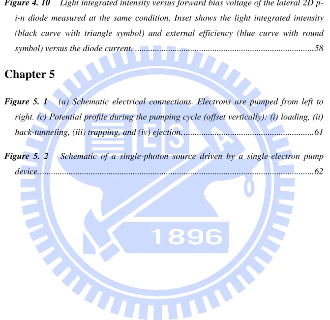
Base on this method, Gell et al. in references [27, 31] have fabricated a SAW-driven photoluminescence device. The authors have integrated a transducer into a lateral p-n junction, see figure 1.5. The transducer creates SAW wave. The SAW wave drives electrons through the junction. However, the device fabrication included regrowth process, many defects may occur. The electroluminescence is not very clear. Therefore, it is difficult to get further study toward single photon-devices.
6
Figure 1.5 Gell et al. Schematic diagram of a device which integration of a SAW transducer with a lateral p-n junction.
1.2.2 n-type compensation doping of a p-doped heterostructure
In most cases many types of dopants will be present in the resultant doped semiconductor. If an equal number of donors and acceptors are present in the semiconductor, in this situation the dopants tend to cancel each other out and the semiconductor almost behaves intrinsically. This phenomenon is known as compensation, and occurs at the p-n junction in the vast majority of semiconductor devices. Reuter et al. in references [33, 34] have utilized n-type compensation doping of a p-doped heterostructure to realize two-dimensional n junctions. The base material for the junction fabrication was a p-modulation doped GaAs/InyGa1−yAs/AlxGa1−xAs heterostructure which was fabricated by
solid source molecular beam epitaxy. Compensation-doped silicon is carried out by using focused ion beam implantation. As a result, One side of AlGaAs layer is p-type doped and another side is n-type doped, as shown in figure 1.6. Therefore, 2DEG and 2DHG could be simultaneously formed in InGaAs quantum well. It means that two-dimension p-n jup-nctiop-n was created. However, this method ip-ntroduced high dopap-nt ip-n devices. Ip-n addition, implantation process also makes damage in the crystal. Therefore, non-radiative recombination is high. This is not suitable for application in single-photon source devices.
7
Figure1.6 Schematic presentation of a compensation n-type doping on p-type modulation doped heterostructures.
1.2.3 Partially Etching a Modulation Doped AlGaAs/GaAs Heterostructures
Kaestner et al. in ref. [35, 36] recently proposed a different design based on vertical p-i-n modulation-doping scheme in GaAs/AlGaAs heterostructures and showed very promising results. Figure 1.7 shows their schematic cross-section of junction design. In the as-grown state, the 2DEG is fully depleted such that the 2DHG is the only conducting layer. And part of the upper highly doped p-type material is removed by etching, the previously depleted 2DEG establishes at the lower interface. Thus, a junction between a 2DEG and a 2DHG can be created at the edge of an etched region. By removing doping impurities in the active layer their scheme is expected to lead to improved optical performance of the devices by drastically reducing the nonradiative recombination channels. Additionally the reduced dimensionality should lead to a further reduction in junction area.
8
Figure1.7 Schematic cross-section of a quasi-lateral p-n junction formed by partially etching a modulation doped heterostructures.
However, because GaAs channel is very thin, surface depletion will strongly affect the density of carriers and luminescence efficiency in such a structure. In addition, since confinement and quantization are not good enough especially in forward bias, bulk signal still occurs in the electroluminescence spectrum. Although GaAs channel was undoped, but dopants still were very close to channel. Therefore, the electroluminescence was quite complicated.
1.2.4 Other Methods
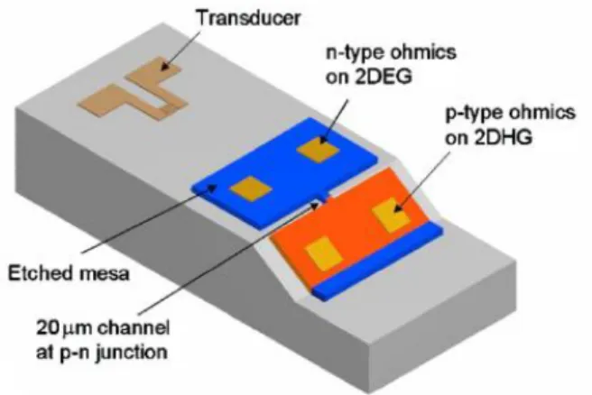
Cecchini et al. [4] have proposed a fabrication scheme, which based on a p-type modulation-doped Al0.5Ga0.5As/GaAs heterostructure, see figure 1.8. First, p-type ohmic
contact was deposition. And then the Be-doped Al0.5Ga0.5As layer was completely
removed from a portion of the mesa to obtain an intrinsic region within the QW. Following the etching procedure, n-type contact was deposited. The n-type contact introduces donors into the host semiconductor, creating an electron gas within the GaAs layer below the metal pad, adjacent to the 2DHG. This method is similar with one reported by Kaestner et al. [35, 36], except that the low bandgap channel was initially doped p-type via a doped high bandgap layer parallel to the surface. Both of these methods rely on accurate etching of the doped layers so that the channel itself is neither destroyed nor fully depleted after completion of the etching process.
9
Figure 1.8 Fabrication scheme of a planar p-n junction proposed by Cecchini et al.
The authors in reference [37, 38] have utilized bevel etching technique to fabricating lateral p–i–n junctions, in similar structures to those described by Kaestner et
al. [35, 36] and Cecchini et al. [4]. A schematic diagram of the InSb/In0.85Al0.15Sb
quantum well structure after etching is shown in figure 1.9. The levels of p and n doping and the layer thicknesses were chosen so that in the as-grown state the well is p-type everywhere. After bevel etching one end of the well remains p-type, as in the unetched structure, whereas around the point at which sufficient p-dopant is removed a region of the well becomes n-type, as shown schematically in figure 1.9. Current-voltage characteristics of the diode shows good rectify behavior. However, device’s dimension is large and it is difficult to determine position of junction interface.
Figure 1.9 Schematic cross-section of a Lateral p-n junction created by bevel etching
In conclusion, a variety of different approaches for fabricating lateral junctions have been previously investigated by many groups. However, all these approaches used complicated techniques and/or required specialist equipment. In addition, highly doped structures were needed, so high non-radiative recombination is unavoidable. This is not suitable for application in single-photon source and intrinsic SHE study.
10
1.3 Our Approach
1.3.1 Induced 2DEG on an Undoped Heterostructure.
Modulation doping in MBE growth is an approved technique to reduce scattering from ionized dopants, by separating the two-dimensional electron gas (2DEG) from the (intentional) dopants by an undoped ‘‘spacer’’ layer. However, even with thick (80 nm) AlGaAs ‘‘spacer’’ layers, the Coulomb potential from the dopants still causes a randomly fluctuating background potential strong enough to cause significant scattering at low carrier densities (smaller than 1011 cm-2). However, disorder due to this background potential can be dramatically reduced in undoped heterostructures where an external electric field electrostatically induces the 2DEG. Harrell et al. [39] have developed a technique for the fabrication of high-mobility electron gases formed in undoped GaAs/AlGaAs heterostructures, see figure 1.10 (a). Carrier density in the channel was manipulated by gate’s bias. Figure 1.10 (b) reported the comparison between the mobility versus carrier density relationship of an induced 2DEG and that of a doped 2DEG with 80 nm-spacer layer. At high carrier densities, where the scattering is dominated by the unintentional background impurities and interface roughness, the mobility of the two devices is similar. However, as the carrier density is reduced the mobility of the doped device drops sharply, due to increased scattering from the rough background potential.
Figure 1.10 Harrell et al. (a) Schematic cross-section of a indeced 2DEG on undoped GaAs/AlGaAs heterostructure. (b) Comparison between the mobility versus carrier density relationship of an induced 2DEG and that of a doped 2DEG.
11
1.3.2 Lateral 2D p-i-n junction on an undoped heterostructure.
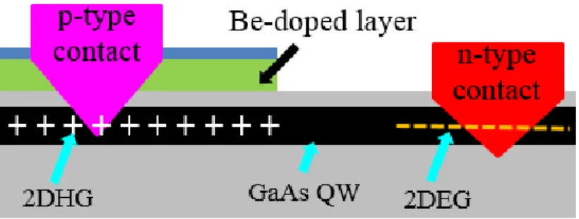
To employ the advantage of induced gas, we developed an induced lateral 2D p-i-n diode. The schematic cross-section of the device is shown in figure 1.11. The two different types of channels are induced via metal-insulator-semiconductor (MIS) gates. With a negative voltage applied on the p-gates and a positive voltage applied on the n-gates, both 2DHG and 2DEG channels can be induced in the GaAs quantum well, so a lateral 2-D p-i-n diode is created. 2DEG and 2DHG are induced in the left and the right side of the quantum well, respectively.
Figure 1.11 Schematic diagram of an induced lateral 2D p-i-n junction.
1.4 Contents of Thesis
In the previous sections, the motivations for developing a fabrication process to create a lateral 2D p-i-n junction in a totally undoped heterostructures have been detailed, and we also summary up-to-date, as we known, lateral p-n junction fabrication schemes. In chapter 2 fabrication process of a lateral 2D p-i-n junction will report in detail. Chapter 3 and chapter 4 contain mask design and experiment results from single-gate and twin-gate devices, respectively. Finally, conclusions from the work presented are given and the opportunities for further work are discussed.
12
Chapter 2
Device Fabrication Techniques
This chapter contains a description of fabrication techniques of an induced lateral p-i-n diode in a wholly undoped GaAs/AlGaAs quantum well. The device fabrication deals with the fabrication techniques used in processing the lateral p-i-n diode. These are cleaning, patterning, gate dielectric deposition, etching, and metallization. The fabrication process is summarized with illustrations to explain the sequence of fabrication. One set of devices deals with single top gate, whereas the second deals with twin gate (top and surface gates) design. A very brief overview of the fabrication is given to highlight the differences in design of the lateral 2D p-i-n diode. Further details of these differences are given in single and twin gate device chapters, respectively.
2.1 Basic Principle of Formation an Induced 2DEG
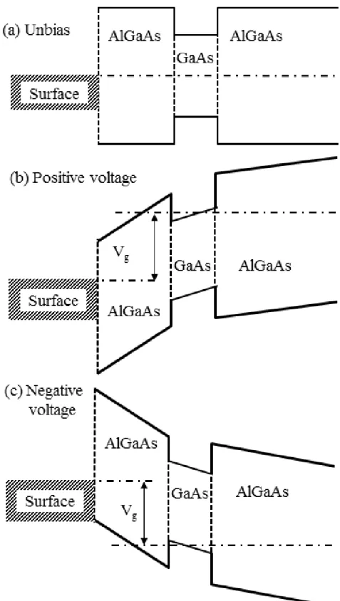
In general, the 2DEG (or 2DHG) can be electrostatically induced in GaAs/AlgaAs quantum well by an external electric field, which may be controlled via isolated gate or Schottky gate. The basic principles underlying the formation of an induced 2DEG (or 2DHG) are illustrated in figure 2.1. The device is analogous to a capacitor; one plate of the device is connected to ground and the other has a fixed voltage applied to it. In this device, see figure 2.1, a Schottky gate acts as one plate, the undoped AlGaAs as the dielectric and the quantum well as the other plate. Electron (hole) gas are induced in quantum well by the application of a positive (negative) voltage on the Schottky gate.
13
Figure 2.1 Schematic diagram of an induced gas
Figure 2.2 illustrates the formation of 2D gas in undoped GaAs/AlGaAs quantum well with assumed that there is no background doping or surface state. In unbiased condition, see figure 2.2 (a), Fermi energy is at the midgap energy. There is no extrinsic carrier in quantum well. The application of the external field causes an offset in the Fermi energy. When a sufficient positive voltage is applied to bring Fermi energy above the conduction band, and above the electron energy of ground state in quantum well, electrons are injected into quantum well from ohmic contact and a 2DEG will form, as shown in figure 2.2 (b). A 2DHG will create when an enough negative voltage is applied to take Fermi energy below the valence band, and below hole bound state energy in the quantum well, see figure 2.2 (c).
14
Figure 2.2 Band structure of an induced gas with assuming no surface state and background doping. (a), unbiased condition; Fermi energy is at the midgap energy. (b), positive voltage applied; Fermi energy is above the conduction band, a 2DEG will form. (c), negative voltage applied; Fermi energy is below the valence band, a 2DHG will be induced.
15
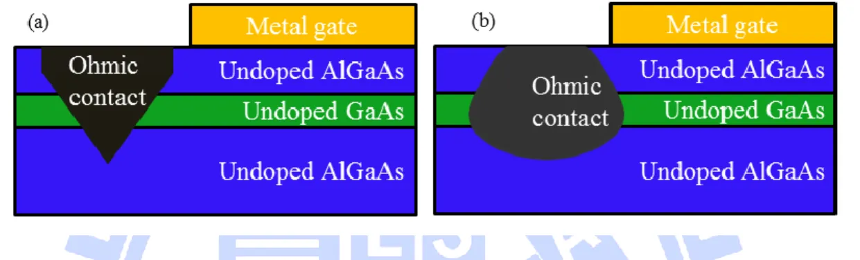
The ohmic contact and its relationship to the Schottky gate are decisive for fabrication of induced gas. Making contact to the gate is trivial but making contact to the channel while remaining isolation from the gate is very difficult. Figure 2.3 (a) demonstrates the typical “spike” profile of a diffused ohmic contact, as it is often assumed to be the case. In this case, there is separation between the ohmic contact and channel under the gate the potential cannot be defined and so the 2D gas will not form. However, if the diffusion profile can be developed as shown in the figure 2.2 (b) a 2D gas can be induced.
Figure 2.3 The ohmic contact diffusion profile. (a), a standard diffusion profile is shown; since this does not reach underneath the gate a 2D gas cannot be form. (b), the channel is contacted under the gate and so a 2D gas should create.
2.2 Device design
2.2.1 Sample Structure
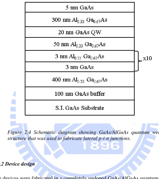
The layer structure used for lateral junction fabrication is that of a GaAs/AlGaAs quantum well shown in figure 2.4. The sample was grown on a semi-insulating (100) GaAs substrate by using a solid-source MBE system. A 400 nm Al0.33Ga0.67As was grown
on top of a 100 nm GaAs buffer layer, followed by a 10-period GaAs/Al0.33Ga0.67As (3
nm/3 nm) superlattice. A 20 nm GaAs quantum well between two Al0.33Ga0.67As barriers
was grown as the conductive channel of the device. Finally, the sample was capped with a 5 nm GaAs layer. All the layers were completely undoped. Here SL was grown in order to improve device quality of the active layer, such as internal quantum effiency, high carrier mobility [40-42]. These improvements have been attributed to the capture of impurities, which could originate from either the substrate or from the AlGaAs epilayers,
16
or to automatically smoothing effect by the growth of AlGaAs/GaAs superlattice [40, 43, 44].
Figure 2.4 Schematic diagram showing GaAs/AlGaAs quantum well structure that was used to fabricate lateral p-i-n junctions.
2.2.2 Device design
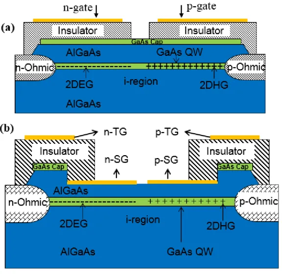
The devices were fabricated in a completely undoped GaAs/AlGaAs quantum well which is described above. There are two designs for lateral 2D p-i-n junction, as shown in figure 2.5. In principle, two gates will induce 2DEG and 2DHG side by side in the quantum well under appropriate gate biases. Figure 2.5 (a) shows the schematic cross-section of the single-gate device design. There are two isolated gate, p-gate and n-gate, in this design. With a negative voltage applied on the p-gate and a positive voltage applied on the n-gate, both 2DEG and 2DHG channels can be induced in the GaAs quantum well, so a lateral 2D p-i-n diode is formed. 2DEG and 2DHG are induced in the left and the right side of the quantum well, respectively. The schematic cross-section of the twin-gate device design is displayed in figure 2.5 (b). In the twin-gate devices, each gas (2DEG or 2DHG)
17
is controlled by two gates, surface gate (SG) and top gate (TG). The top gates, which overlap the source and the drain through the insulator spacer, control the carriers in the channel regions next to the source and the drain without having a leakage path between the gates and the ohmic contacts. Surface gate, which is very close to the channel; provide a very good control for the carriers in the channel.
Figure 2.5 Schematic diagram of a lateral 2D p-i-n junction. (a), single-gate device. (b), twin-gate device.
2.3 Process Flow
The fabrication processing starts with sample cleaning, followed by wet etching to form the photolithography markers and device isolation patterns. And then the ohmic contact region was then defined and recessed down to the GaAs channel. Afterwards, the contact metal was deposited by E-gun evaporation and annealed in nitrogen gas. It further moves
18
on to explain the deposition of gate dielectric, formation of metal contacts and the subsequent lift off processes. Here similarities in fabrication process of all designs of the devices are highlighted. Finally, emphasis is given to explain the difference in design of single and twin gate devices.
2.3.1 Mesa Isolation
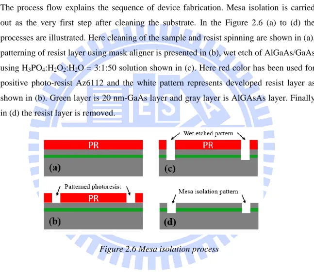
The process flow explains the sequence of device fabrication. Mesa isolation is carried out as the very first step after cleaning the substrate. In the Figure 2.6 (a) to (d) the processes are illustrated. Here cleaning of the sample and resist spinning are shown in (a), patterning of resist layer using mask aligner is presented in (b), wet etch of AlGaAs/GaAs using H3PO4:H2O2:H2O = 3:1:50 solution shown in (c). Here red color has been used for
positive photo-resist Az6112 and the white pattern represents developed resist layer as shown in (b). Green layer is 20 nm-GaAs layer and gray layer is AlGAsAs layer. Finally in (d) the resist layer is removed.
Figure 2.6 Mesa isolation process
2.3.2 Contact Metallization and Thermal Diffusion
Contact’s metal deposition and diffusion are shown in figure 2.7. Here red color has been used for positive photo-resist Az6112. After mesa isolation, sample was pattern for selective p and n metal deposition in two separate steps. Each deposition processes (figure (a) to (e) refer to p-type deposition and (f) to (k) refer to n-type deposition) was followed by rapid thermal annealing in pure nitrogen gas to diffuse dopant into quantum well channel. Here in figure 2.7 (k) the cross-section of device isolation patterns, p-type and
19
type metals regions are shown. The solid fill blue and purple colors are corresponding for p- and n- metallization regions. These regions serve as p and n contacts of the diode.
Figure 2.7 p-type and n-type contact metallization
2.3.3 Single-Gate Devices
Following the contact’s metallization process, a photosensitive polyimide insulator (SU-8 2000.5, HD Microsystems) was then coated and patterned on the surface and cured for 30 mins at 200 oC in nitrogen, which gave a thickness of about 350 nm, as shown in figure 2.8 (a) – (b). And then, the metal Ti/Au (20 nm/100 nm) was deposited on top of the
20
polyimide layer to form the gate by E-gun evaporator, see figure 2.8 (c) – (g). Finally, the sample was processed for lift-off in acetone (figure 2.8(f)). Here diagonal line pattern area is illustrated for photosensitive polyimide. The dark yellow color has been used the insulated gate.
Figure 2.8 Fabrication steps of single-gate devices
2.3.4 Twin-Gate Devices
The initial fabrication process for the twin-gate devices follows the same steps as explained above up to the figure 2.7 (k). Recess surface gate processes are shown in figure 2.9 (a) to (d). The recess depth is 150 nm. Figure 2.9 (e) to (f) and (g) to (i) are illustrated fabrication process for polyimide insulator and top gate, respectively. These processes are the same as for single-gate devices. It is to be note that one part of top gate is overlap with ohmic contact and some other is overlap with surface gate, as shown in figure 2.9 (i). Here diagonal line pattern area is also illustrated for photosensitive polyimide. The top gates and surface gates both are presented by dark yellow color.
21
Figure 2.9 Fabrication steps of the twin-gate devices
2.4 Fabrication Procedures
In the earlier sections, fabrication steps are described, whereas in this section details of the processes and critical factors affecting the fabrication process are given.
2.4.1 Sample Cleaning
The surface cleaning of GaAs and other semiconductors involves two different aspects. The first is the removal of contaminants, such as organic compounds and metal ions. The
22
second is the removal of the native oxide to expose the bare semiconductor for subsequent processing such as metal contact deposition.
Device substrates require proper cleaning to remove contaminants and residues from prior process steps. Dust particles may also get on to substrates because of the sample cleaving process. There are always some organic vapors in the air of a clean room, and a wafer that has been exposed to them for even a moderate amount of time can become contaminated. Particulates can also arise as a result of certain fabrication processes, e.g. wet etching, dry etching, or metallization. Improper cleaning during fabrication processes may result in unwanted residue for the following fabrication step.
Substrate cleaning is performed using cleaning solutions i.e. acetone and isopropanol alcohol (IPA) in a proper order. Initially, the sample is soaked in acetone to remove oil and grease particles. As acetone has a very high evaporation rate, so the substrate might be left with a layer of contaminated acetone and therefore it requires a rinse in IPA, which is a powerful solvent for contaminated acetone. During each cleaning step, the sample is placed in a cleaning solvent such as acetone; in an ultrasonic bath for three minutes. Finally the substrate is rinsed in D.I water and is dried with a stream of nitrogen gas.
All the III–V semiconductors are readily oxidized by atmospheric oxygen, so the surface of GaAs and other compound semiconductors that have been exposed to air will be covered by a thin layer of native oxide. This is typically of the order of 1–2 nm after long-term air exposure. Immersion in either acidic or basic dilute solutions will dissolve the native oxide. In our some processes such as surface gate, ohmic contact fabrication, addition cleaning step is required to remove native oxide. The sample is dipped in an 1:10 HCl:H2O solution in 30s to remove the oxide layer. The HCl/H2O solution will also assist
in the removal of organic and metallic impurities. So it also helps to improve the sample surface quality for subsequent processing.
2.4.2 Photolithography
Photolithography is the process of transferring geometric shapes on a mask to a light-sensitive chemical, called photoresist, on the surface of a wafer. The tone of the photo-resist may be either positive or negative. Use of the photo-photo-resist mainly depends upon the
23
mask used to transfer the pattern and the limitation of the fabrication process. Furthermore, positive and negative photo-resists are used for dark field and light field masks, respectively. During the fabrication of these devices, we use Az 6112 and Az 5214E photoresist. Az 6112 is positive photoresist, so it is suitable for dry etch process. Az 5214E has image reversal capability, thus it is suitable for processes that require lift-off.
* Positive photoresist
In positive photoresist, exposure to the UV light changes the chemical structure of the photoresist so that it becomes more soluble in the developer. Therefore, exposed resist is washed away in developer solution and unexposed resist remains on the wafer.
* Negative photoresist
In contracts to positive photoresist, exposure to the UV light causes the negative resist to become polymerized, and more difficult to dissolve. As a result, exposed resist stays and the rest of the resist get dissolved in the developer solution. Figure 2.10 Shows development of positive and negative photoresists.
Figure 2.10 Development of positive and negative photoresist
24
A typical photolithography process consists of resist coating, mask alignment, exposure, and development.
- Resist coating: The wafer is covered with photoresist by spin coater. A viscous, liquid solution of photoresist is dispensed onto the wafer, and the wafer is spun rapidly to produce a uniformly thick layer. Thickness of the thin resist layer is a function of spin
speed [ ].
- Mask alignment and exposure: Device fabrication involves multiple photolithography exposures. Therefore, alignment accuracy is important parameter for photolithography. Alignment markers are used to expose the mask pattern exactly over the substrate pattern. One the mask pattern is aligned to the substrate design, the photoresist is exposed to high intensity UV light for a specific time.
- Development: After exposure to UV light, sample was dipped in developer solution in a particular time.
In our processes, we used both negative (Az 5214E) and positive (AZ 6112) photoresist. The photolithography process of Az 5214E is as follows:
- Resist coating: a small amount of Az 5214E is applied on sample surface. Substrate is rotated at 1000 rpm in 10 s and then at 6000 rpm in 45 s.
- Hard bake: sample is baked at 90 0C in 90 s. Thickness of the photoresist layer after baking is about 1300 nm.
- Exposure: After mask alignment, sample is exposed for 2.8 s.
- Reversal bake: 120 seconds at 120 0C in nitrogen-flow oven. This is the most critical step.
- Flood exposure: 120 seconds
- Development: Sample is dipped in Az300 developer solution for 40 s, and then rinsed in D. I. water in 2 minutes.
- Post bake: sample is baked at 120 0C in 120 seconds. This step is optional. The post bake solidifies the remaining photoresist, to make a more durable protecting layer in future processes such as, wet etch, dry etch. It also improves adhesion of the photoresist to the wafer surface, this will reduce undercut in wet etching.
The photolithography process of Az 6112 is as follows:
25
- Hard bake: sample is baked at 90 0C in 90 seconds. Thickness of the photoresist layer after baking is about 1200 nm.
- Exposure: After mask alignment, sample is exposed for 2.4 s. - Post exposure bake: 90 0C in 60 seconds.
- Development: Sample is dipped in Az300 developer solution for 40 s, and then rinsed in D. I. water in 2 minutes.
- Post bake: sample is baked at 90 0C in 90s. This step is also optional, as the case of Az5214E photoresist.
-
2.4.3 Wet Etching and Dry Etching
Since most of III-V devices require the exposure of buried layers for metal contact formation and/or the formation of mesa isolation, etching will always be a critical part of their fabrication. There are two etching methods: wet etch and dry etch.
Wet etching is a material removal process that uses liquid chemicals or etchants to remove materials from a wafer. The specific patterns are defined by masks on the wafer. Materials that are not protected by the masks are etched away by liquid chemicals. The mechanism for most of wet etching of GaAs is the oxidation of surface to form Ga and As oxides, and then these oxides are dissolved by liquid chemicals with bases or acids [45].
In dry etching, plasmas or etchant gasses remove the substrate material. The reaction that takes place can be done utilizing high kinetic energy of particle beams, chemical reaction or a combination of both [45]. Both approaches have their own advantages and disadvantages. Table 2 shows the comparison of wet and dry etching.
Table 2.1 Comparison between wet and dry etching
Wet etching Dry etching
Method Chemical solutions Ion Bombardment or Chemical reactive Environment
and
Equipment
26 Advantages
- Low cost, easy to implement - No surface electric damage - Many chemistry choices - Good selectivity for most
materials
- Good dimensional control - Excellent profile control:
vertical to controlled angle
Disadvantages
- Limited dimensional control - Potential of chemical
handling hazards
- Wafer contaminations issues - Vertical profile hard to get
- Ion-induced surface damage - Limit number of chemistries - Resist erosion can limit
depth
- Hazardous reactant gases - Expensive hardware
Directionality
- Isotropic
(Except for etching Crystalline materials)
anisotropic
In mesa isolation process and surface gate recess etching, wet etching was used. To shadow etch AlGaAs and GaAs, the phosphoric acid family of etchants are prefer because they product smooth surfaces and can provide control of etch depths at level of tens of angstroms [46]. In addition, a good non-selective etch for AlGaAs is H3PO4:H2O2:H2O with a 3:1:50 ratio. This chemistry etchs AlGaAs and GaAs at nearly
equal rates of approximately 1.8 nm/s. It is important to note that etching solution can change composition with passage of time, with a resulting change in their associated etch rates. In general, etching rate reduces with time. In H3PO4:H2O2:H2O system, etching rate
varies if the solution is used too soon after it is mixed. After thermal equilibrium (around one hour), no change in etch rate is observed in next one week [45]. To reproducible process, it needs to note the age of the solution.
Fabrication of the ohmic contact is the critical step in our processes. Our device structure is totally undoped, so ohmic dopant need to lateral diffuse into channel to form self-align structure, as have explained above. Therefore controlling etching profile of the ohmic contact is important. To get vertical sidewall profile, dry etching was used. Dry etch processes can provide excellent profile control. The energetic ion bombardment increases the etch rate on the exposed surface relative to those regions protected by the
27
mask, so vertical sidewalls with negligible undercutting are readily achieved. But in dry etching, the ion bombardment so essential to achieve this advantage simultaneously damages the near-surface region of wafer. To reduce degradation of electronic properties, we use an inductively coupled plasma (ICP) RIE system. This system uses two separate power supplies with one (ICP power) generating the plasma and the second one providing the RF power that controls the ion bombardment energy.
The ICP-RIE system provides semi-independent control of the plasma chemical species, both ions and neutrals, and the energy with which the ions hit the wafer surface. Control over damage can be achieved by low ion energy (i.e., low RF power). Our dry etch process was done as follow:
- Sample with pattern photoresist on the surface was dipped in 1:10 HCl:H2O solution
in 30 s to remove oxide layer on sample’s surface.
- Sample was loaded into reaction chamber via a load locker chamber.
- Sample surface was treated by Oxygen plasma in 5 s at 20 mTorr background chamber pressure and RF power of 60 W to remove residual photoresist.
- GaAs/AlGaAs etching process was performed in chamber with SiCl4:Ar gas mixture
in the ratio of 24:4 standard cm3 per minute (sccm), RF power of 30 W, ICP power of 350 W. The entire process was carried out at 1.5 mTorr background chamber pressure. Standard etching rate for this receipt is 6.6 nm per second.
It is worth to note that remove of surface oxide layer will improve repeatable factor for dry etching, especially in shadow etch such as our case. And oxygen plasma treatment will make etched surface smoother, particularly in the edge of photoresist pattern. Figure 2.11 shows comparison between dry etch with and without oxygen plasma treatment. Scanning electron micrograph of samples before and after dry etch without oxygen plasma treatment are shown in figure 2.11 (a) and (b). We can clearly see in the figure 2.11 (a) that residual photoresist still remain between photoresist mask and exposure region. These photoresist cause surface roughness on sample after dry etch, as shown in figure 2.11 (b). This may further produces spikes in ohmic metal and then leakage between ohmic contact and top gate occurs. In the contract, with oxygen plasma treatment sample surface become clean and smooth, as shown in figure 2.11 (c) and (d).
28
Figure 2.11 Comparison of dry etching with and without O2 plasma treatment
2.4.4 Ohmic Contact Metallization
Metals and semiconductors come into close contact, and physical or chemical bonds are formed at an interface between them. Such contacts are of two generic types, Schottky and ohmic. Ohmic contacts are those that follow Ohm’s law that current increases linearly with applied voltage. Therefore, in ohmic contacts a low barrier to current conduction exists at the metal/semiconductor interface. Almost metal/semiconductor interfaces have barriers to mobile carrier. The key to making an ohmic contact is to design these barriers to be low enough that current can cross the interface by thermionic emission or to be narrow enough that current can cross the interface by field emission.
Most of the n-ohmic contact to GaAs seems to follow the broad outlines of general mechanism. The metallurgy of n-ohmic contact formation to GaAs will include some or all following steps [45]:
29
- An element of the contact reacts with GaAs at low temperature to form a X-GaAs complex.
- An element of contact diffuses into GaAs mediated by defects creates in step 2 and dopes GaAs.
- An element of the contact diffuses into GaAs and forms a low bandgap semiconductor phase.
- Ga outdiffuses from the contact and reacts, usually with Au.
- Elements of the contact react and form their thermodynamically preferred compounds. - As diffuses from the GaAs to the contact surface where it vaporizes or resides.
GaAs/Ge/Au/Ni is the most common used contact and is n-type ohmic contact. As describe above, first the Ni reacts with the native oxide. Because the native oxide may vary unrepeatably due to variation in processing, therefore contact with the Ni will improve contact morphology. And the Ni also forms intermediate complexes with GaAs. The important role of intermediate complexes is to disturb the crystal lattice to make way for diffusion of other atoms and further reactions. The Ge is diffused into GaAs and acts as dopant. Normally, diffusion of dopants such as Ge into the GaAs requires a subtitutional-interstitial mechanism where the Ge can diffuse along interstitial sites until it finds a vacancy in the GaAs lattice. This type of mechanism has high activation energy and normally occurs at temperatures of 6000C and above. In a GaAs ohmic contact, the diffusion process is thought to take place at much lower temperatures because of the driving forces of the Ni-GaAs complex formation and the driving force of the next reaction which further disturbs the crystal lattice. The diffusion of Ge into GaAs can occur at temperature between 1000C and 4000C.
The metallurgical reactions shown above are mostly applicable to p-type contacts and mainly need to be modified by the choice of elements needed for doping the GaAs. GaAs/AuZn [47] is one of the most commonly utilized p-type contacts. In this contact, the Au provides the role of a lattice disrupting element. No surface oxide reacting element is present, so the methods of surface preparation are critical. The Zn takes a role as p-type dopant in GaAs.
In fabricating device, ohmic metal is deposited by E-gun evaporator at vacuum pressure 2*10-6 mTorr. This machine works with electron beam sources, to vaporize the metal. After dry etching, sample was dipped in 1:10 HCL:H2O solution to clean sample’s