Manuscript submitted March 12, 2007; revised manuscript received June 25, 2007. Available electronically October 22, 2007.
Negative bias temperature instability共NBTI兲 is known to be a critical reliability concern and represents one of the major bottle-necks for product lifetime in nanoscale p-channel metal-oxide-semiconductor field-effect transistors 共PMOSFETs兲.1-7 Usually the creation of interface traps and positive fixed charges by the disso-ciation of Si–H bonds at the SiO2/Si interface could cause a large threshold voltage shift, thus diminishing the current drive and trans-conductance of the device, and may eventually lead to circuit mal-function.
Using process techniques to induce uniaxial strain in the channel for enhancing carrier mobility and thus drive current has recently received a lot of attention.8-16 Several approaches have been re-ported to induce compressive channel strain beneficial for improving the hole mobility, including embedded SiGe in the source/drain 共S/D兲 region10,11
and the SiN contact etch-stop layer 共CESL兲.12-14 The latter approach is typically carried out by depositing the SiN layer using plasma-enhanced chemical vapor deposition共PECVD兲. In contrast to the complex and costly SiGe refill scheme, the sim-plicity and maturity of the PECVD SiN 共PE-SiN兲 process seem much more attractive and practical. Although strain channel could boost device performance, the strain energy stored in the channel and a high amount of hydrogen species contained in the PE-SiN layer could potentially worsen the NBTI reliability.15,16To address this issue, this paper presents a different approach by inserting a thin buffer layer prior to SiN capping for suppressing hydrogen diffusion into the channel.
Device Fabrication
The PMOSFETs in this study were fabricated on 6 in. n-type Si wafers with conventional local oxidation of silicon共LOCOS兲 isola-tion. Gate oxide with a thickness of 3 nm was grown in a vertical furnace in O2at 800°C. After gate oxide growth, a 200 nm thick polycrystalline silicon 共poly-Si兲 was deposited by low-pressure chemical vapor deposition共LPCVD兲, followed by standard plasma gate etch to form the patterned gate. Afterward, standard procedures were applied to form tetraethoxysilane共TEOS兲 spacer and S/D junc-tions. Subsequently, a rapid thermal annealing at 900°C for 30 s was performed to activate dopants in the gate and S/D regions. A 300 nm thick PE-SiN was then deposited onto the device surface, followed by the deposition of TEOS passivation by PECVD. For some SiN-capped samples, a 3 nm thick HfO2buffer layer deposited by metallorganic chemical vapor deposition 共MOCVD兲 was capped prior to SiN deposition共denoted as HfO2-buffered split兲. The
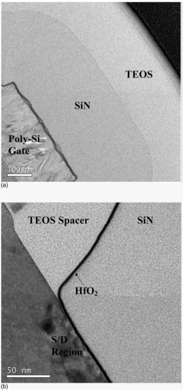
thick-ness measured from cross-sectional transmission electron
micro-scope共TEM兲 pictures for SiN and HfO2layer is⬃310 and 3 nm,
respectively, as shown in Fig. 1a and b. Contact holes and metalli-zation processes were subsequently performed. Finally, the process-ing steps were completed with a formprocess-ing gas anneal at 400°C. Elec-trical characteristics were measured using an Agilent 4156 system. NBTI stress measurements were performed using a temperature-regulated hot chuck at 125°C. Interface traps were evaluated using charge pumping method with fixed amplitude of 1.5 V at 1 MHz.
Devices Characteristics
The stress of PE-SiN layer with and without an HfO2buffer layer 共3 nm兲 was first examined by probing blanket monitor samples de-posited on Si wafers. We confirmed that the stress was compressive in nature with a magnitude of around −700 MPa for all samples, irrespective of the HfO2presence. This indicates that the insertion of such ultrathin buffer layer will not relax the strain introduced by the SiN capping.
Figure 2 compares transconductance data for all splits with chan-nel width/length共W/L兲 = 10/0.4 m. It can be seen that the trans-conductance of all SiN-capped samples, with or without HfO2buffer layer, depicts significant and identical enhancement of⬃26% with respect to that of the control counterparts without SiN capping. Out-put characteristics of PMOSFETs are shown and compared in Fig. 3. Similar enhancement trend in the drive current is also observed for the two SiN-capping splits. These findings confirm the results ob-tained in stress measurements that the insertion of an ultrathin HfO2 buffer layer does not compromise the performance enhancement in-duced by the SiN capping.
Figure 4 shows the percentage increase in transconductance for SiN-capped and HfO2-buffered splits, compared to the control split,
as a function of channel length. Each data represents the mean mea-surement result performed on eight devices in Fig. 4. Note that the strain is distributed locally inside the channel region and is concen-trated near the source and drain region.17,18As the channel length becomes shorter, the distance from the edge of the spacer to the center of the channel becomes shorter; thus, the induced strain be-comes stronger. Therefore, we can see that the transconductance enhancement increases with decreasing channel length, a unique feature for uniaxial strain induced by SiN capping.17,18Moreover, the induced compressive strain is not relieved by the insertion of the buffer layer. Capacitance–voltage共C-V兲 characteristics of all splits of samples coincide altogether, as shown in Fig. 5. Negligible dif-ferences in oxide thickness among these devices are observed, indi-cating that the above-mentioned observations, indeed, are not caused by the oxide thickness difference among splits. The subthreshold characteristics of PMOSFETs for all splits of samples are shown in Fig. 6. We can see that the subthreshold characteristics are not af-z
fected by the presence of SiN and HfO2-buffer layers. This is further convinced in Fig. 7, in which the mean value of the extracted sub-threshold swing from ten devices is the same for the three splits of devices.
NBTI Characteristics
Figure 8 shows the results of NBTI stress performed at three different gate biases for HfO2-buffered samples. It can be seen that
larger gate bias leads to larger threshold voltage shift共⌬Vth兲, imply-ing that more defects are beimply-ing generated at higher bias. The shift curves show a fractional power-law dependence on time 共⌬Vth
⬀ tn兲, and the values of the exponent 共n兲 are roughly 0.3 for these
samples. A comparison among the three splits of samples is given in Fig. 9, under the same stress condition, VG− Vth= −3.5 V. It is
seen that the SiN-capped split depicts much larger⌬Vthas compared
to the control split. Such degradation is relieved when the HfO2 buffer layer is added. After 1000 s stress, the⌬Vthis 46.12, 197.23,
and 274.72 mV for control, HfO2-buffered, and SiN-capped splits,
respectively. Figure 10 compares the increase in interface state den-sity共⌬Nit兲 and subthreshold swing shift 共⌬Swing兲 for all samples extracted using the charge pumping technique. Basically the trends are similar to those shown in Fig. 9. Figure 11 shows the transcon-ductance degradation ratio as a function of stress time. The trans-conductance degradation ratio for SiN-capped split depicts the se-verest degradation among all three splits, reaching 16% after 1000 s stress, implying that NBT stress grossly degrades the device perfor-mance and negates the benefit gained from the SiN capping, though the SiN capping can enhance carrier mobility in a fresh device. More importantly, the transconductance degradation is alleviated for HfO2-buffered split. These results clearly indicate that the use of
PE-SiN capping may aggravate NBTI, while the insertion of HfO2
buffer layer can be helpful to relieve the situation. In short, although the capping of SiN tends to worsen the device reliability
character-Figure 1. Cross-sectional TEM pictures of HfO2-buffered samples taken in
共a兲 the passivation region and 共b兲 the spacer region. The thickness of SiN and HfO2buffer layer is roughly 310 and 3 nm, respectively.
Figure 2. 共Color online兲 Transconductance vs VG− Vth for all splits of
samples. For the SiN-capped devices, with or without inserting the buffer layer, the transconductance is clearly increased with respective to the control.
Figure 3.共Color online兲 Output characteristics of PMOSFETs for all splits.
The insertion of the HfO2buffer in the SiN-capped device does not compro-mise the drive current enhancement with respective to the control.
istics, the insertion of a thin HfO2buffer layer between the gate and
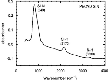
the SiN can effectively shield the device against the degradation. These findings are postulated to be related to the hydrogen spe-cies contained in the PE-SiN layer. Owing to the use of SiH4and
NH3as the reaction precursors, the deposited SiN contains abundant
hydrogen, as confirmed by the FTIR analysis shown in Fig. 12. In Fig. 12, visible H-bonding signals from the PE-SiN layer can be detected by Fourier transform infrared spectrometer共FTIR兲, indicat-ing that the film indeed contains a substantial amount of hydrogen. It thus acts as a diffusion source for hydrogen to diffuse into the chan-nel during the deposition process and subsequent thermal cycles, including the forming gas anneal. Although hydrogen can effectively passivate the dangling bonds at the SiO2/Si interface, the passivated Si–H bonds are more easily broken during subsequent stressing; thus, the voluminous hydrogen species aggravate NBTI. The inser-tion of a thin HfO2buffer layer between the gate and SiN capping
can effectively suppress the diffusion of hydrogen into the gate ox-ide and oxox-ide/channel interface, resulting in less broken Si–H bonds and thus less newly generated interface states during stressing, as compared to the SiN-capped split. It is well known that the
depos-ited HfO2 layers typically contain a high density of structural defects.19,20We postulate that these defects tend to trap the hydrogen
Figure 4.共Color online兲 Transconductance increase vs channel length. Each
data point represents the mean measurement result performed on eight de-vices.
Figure 5. 共Color online兲 Capacitance–voltage 共C–V兲 characteristics of all
splits. The curves are almost coincided with each other, indicating that the oxide thickness difference among the three splits is negligible.
Figure 6.共Color online兲 Subthreshold characteristics of all splits.
Figure 7. Subthreshold swing of all splits.
Figure 8. 共Color online兲 Threshold voltage shift 共⌬Vth兲 vs stress time for
species diffusing during the SiN deposition and subsequent thermal cycles. As a result, the inserted HfO2acts as a diffusion barrier for hydrogen.
In this study, the thickness of the HfO2buffer is fixed at 3 nm. Such a thin buffer layer would not compromise the performance gain obtained from the channel strain. In the meantime, the immu-nity against NBTI degradation is clearly demonstrated. However, it should be noted that the optimum thickness is yet to be determined. In this aspect more effort is in progress, and it is expected that further improvement in NBTI immunity is possible when the con-dition is optimized.
Conclusion
SiN-capped PMOSFETs with a thin HfO2buffer layer were fab-ricated and characterized in this study. Although the SiN layer tends to worsen the NBTI characteristics, our results demonstrate the use-fulness of inserting a buffer layer in relieving the situation. Further-more, no performance gain from the channel strain is compromised at all as the buffer layer is inserted. Such improvement is ascribed to the suppression of hydrogen diffusion from the SiN to the gate oxide and the oxide/channel interface with the insertion of the buffer layer.
Acknowledgments
We thank the National Nano Device Laboratories共NDL兲 for as-sistance in device fabrication and Ying-Hung Chen for his help dur-ing the course of this study. This work was supported in part by the National Science Council of the Republic of China under contract no. NSC 95-2221-E-009-297.
National Chiao-Tung University assisted in meeting the publication costs of this article.
References
1. S. Ogawa, M. Shimaya, and N. Shiono, J. Appl. Phys., 77, 1137共1995兲. 2. C. H. Liu, M. T. Lee, C. Y. Lin, J. Chen, Y. T. Loh, F. T. Liou, K. Schruefer, A. A.
Katsetos, Z. Yang, N. Rovedo, et al., Jpn. J. Appl. Phys., Part 1, 41, 2423共2002兲. 3. D. K. Schroder and J. A. Babcock, J. Appl. Phys., 94, 1共2003兲.
4. X. J. Zhou, L. Tsetseris, S. N. Rashkeev, D. M. Fleetwood, R. D. Schrimpf, S. T. Pantelides, J. A. Felix, E. P. Gusev, and C. D’Emic, Appl. Phys. Lett., 84, 4394 共2004兲.
5. M. A. Alam and S. Mahapatra, Microelectron. Reliab., 45, 71共2005兲. 6. J. Ushio, T. Maruizumi, and K. K-Abdelghafar, Appl. Phys. Lett., 81, 1818共2002兲. 7. S. Mahapatra, M. A. Alam, P. B. Kumar, T. R. Dalei, and D. Saha, Tech. Dig. - Int.
Electron Devices Meet., 2004, 105.
8. S. Pidin, T. Mori, K. Inoue, S. Fututa, N. Itoh, E. Mutoh, K. Ohkoshi, R. Naka-mura, K. Kobayashi, K. KawaNaka-mura, et al., Tech. Dig. - Int. Electron Devices Meet.,
2004, 213.
9. K. Mistry, M. Armstrong, C. Auth, S. Cea, T. Coan, T. Ghani, T. Hoffmann, A. Murthy, J. Sandford, R. Shaheed, et al., Symp. VLSI Tech. Dig., 2004, 50. 10. K. Ota, T. Sanuki, K. Yahashi, Y. Miyanami, K. Matsuo, J. Idebuchi, M. Moriya, K.
Nakayama, R. Yamaguchi, H. Tanaka, et al., Symp. VLSI Tech. Dig., 2006, 78. 11. K. J. Chui, K. W. Ang, A. Madan, H. Wang, C. H. Tung, L. Y. Wong, Y. Wang, S.
F. Choy, N. Balasubramanian, M. F. Li, et al., Tech. Dig. - Int. Electron Devices
Meet., 2005, 493. Figure 9.共Color online兲 Threshold voltage shift 共⌬Vth兲 vs stress time for all
three splits with VG− Vth= −3.5 V at 125°C.
Figure 10.共Color online兲 Interface state generation 共⌬Nit兲 and subthreshold
swing degradation 共⌬Swing兲 vs stress time for all three splits with VG − Vth= −3.5 V at 125°C.
Figure 11.共Color online兲 Transconductance degradation vs stress time for
all three splits with VG− Vth= −3.5 V at 125°C.
Figure 12. Bonding signals of PECVD-SiN layer by Fourier transform