Highly-directional emission patterns based on near single guided mode extraction
from GaN-based ultrathin microcavity light-emitting diodes with photonic crystals
Chun-Feng Lai, Hao-Chung Kuo, Peichen Yu, Tien-Chang Lu, Chia-Hsin Chao, Hsi-Hsuan Yen, and Wen-Yung Yeh
Citation: Applied Physics Letters 97, 013108 (2010); doi: 10.1063/1.3459970
View online: http://dx.doi.org/10.1063/1.3459970
View Table of Contents: http://scitation.aip.org/content/aip/journal/apl/97/1?ver=pdfcov Published by the AIP Publishing
Articles you may be interested in
Emission aperture size limited the guided mode extraction characteristics of GaN-based ultrathin-film photonic crystal micro-light-emitting diodes
Appl. Phys. Lett. 101, 023109 (2012); 10.1063/1.4734509
High extraction efficiency light-emitting diodes based on embedded air-gap photonic-crystals Appl. Phys. Lett. 96, 031108 (2010); 10.1063/1.3293442
Directional light extraction enhancement from GaN-based film-transferred photonic crystal light-emitting diodes
Appl. Phys. Lett. 94, 123106 (2009); 10.1063/1.3106109
Directional emission control and increased light extraction in GaN photonic crystal light emitting diodes Appl. Phys. Lett. 93, 103502 (2008); 10.1063/1.2978068
Enhanced light extraction from GaN-based green light-emitting diode with photonic crystal Appl. Phys. Lett. 91, 181109 (2007); 10.1063/1.2804005
This article is copyrighted as indicated in the article. Reuse of AIP content is subject to the terms at: http://scitation.aip.org/termsconditions. Downloaded to IP: 140.113.38.11 On: Wed, 30 Apr 2014 10:06:19
Highly-directional emission patterns based on near single guided mode
extraction from GaN-based ultrathin microcavity light-emitting
diodes with photonic crystals
Chun-Feng Lai,1,2Hao-Chung Kuo,1,a兲Peichen Yu,1Tien-Chang Lu,1Chia-Hsin Chao,2 Hsi-Hsuan Yen,1and Wen-Yung Yeh2
1
Department of Photonics, Institute of Electro-Optical Engineering, National Chiao-Tung University, Hsinchu 300, Taiwan
2
Electronics and Optoelectronics Research Laboratories, Industrial Technology Research Institute, Hsinchu 310, Taiwan
共Received 24 February 2010; accepted 12 June 2010; published online 9 July 2010兲
This study investigates the distribution of highly-directional far-field emission on GaN-based ultrathin microcavity light-emitting diodes共uMCLEDs兲 with photonic crystals 共PhCs兲. The ultrathin 550 nm cavity, PhC lattice constant of 370 nm, and hole depth of 250 nm in the GaN PhC uMCLED provide near single guided mode extraction and a pattern of high directionality radiation. Angular-spectral-resolved electroluminescence measurements reveal photon-band structure agreement with the fundamental mode effective refractive index dispersion curve. In addition, GaN PhC uMCLED increase the output power extraction efficiency by 145.9%共⬃2.46⫻兲 compared with GaN non-PhC uMCLED, and a directional far-field emission pattern at half intensity of nearly ⫾15°. © 2010 American Institute of Physics. 关doi:10.1063/1.3459970兴
Developing next-generation light-emitting diodes 共LEDs兲 for applications such as projector displays, backlight displays, and automobile headlights requires further im-provement in light extraction efficiency共LEE兲 and direction-ality of far-field emission distribution.1Several schemes have been demonstrated using photonic crystals共PhCs兲 to control the direction of far-field emissions and enhance LEE from microcavity 共thin-film兲 LEDs 共MCLEDs兲.2–4 The surface PhC did not closely interact with the lower-order guided modes of GaN PhC MCLEDs, due to the thickness of the GaN. Although many studies have investigated improving LEE in GaN-based MCLEDs with PhC structures, there has been little research into controlling the distribution of direc-tional far-field emission. As yet, no studies have explored the highly-directional far-field emission patterns of blue GaN-based PhC ultrathin MCLEDs共uMCLEDs兲 with an ultrathin cavity thickness of 550 nm.
This study demonstrated highly-directional light extrac-tion emission, based on near single guided mode from GaN-based PhC uMCLEDs. Angular-spectra-resolved electrolu-minescence共EL兲 measurement shed light on the behavior of guided mode extraction from GaN uMCLEDs with and with-out PhC structures. The photon-band structure correlated with the dispersion curve of the guided mode effective re-fractive index. This work approached the highly-directional radiation pattern of GaN PhC MCLEDs with ultrathin cavity length and deep PhC.
The blue GaN-based LED wafers used in this study con-sist of a 30-nm GaN nucleation layer, a 2-m un-doped GaN buffer layer, a 2-m Si-doped n-GaN layer, a 120 nm InGaN/GaN multiple quantum well 共MQW兲 active region with 12 periods 共dominant wavelength o= 455 nm兲, a 20-nm Mg-doped p-AlGaN electron blocking layer, a 125-nm Mg-doped p-GaN contact layer. After the epitaxial
wafer bonding, the sapphire substrate was removed with the laser lift-off technique. The resulting structure was then thinned down by chemical-mechanical polishing to obtain the GaN effective cavity with thickness 550 nm 共T⬃3兲. The associated mesas were etched further down to the bond-ing metal interface to provide sbond-ingle chip isolation. Next, to fabricate PhC on the n-GaN surface, the PhC with a square lattice of circular holes was then defined by holography li-thography. PhC holes were etched by inductively coupled plasma into the top n-GaN surface to a depth around t = 100 共shallow-PhC兲 and 250 共deep-PhC兲 nm, respectively. The PhC lattice constant a value is 370 nm and the hole diameter d fixed to the ratio d/a=0.7. The schematic of the GaN PhC uMCLED presented in this letter is shown in Fig.
1. Finally, a patterned Cr/Au electrode was deposited on the n-GaN and Si substrate background as the n-type and p-type contact layer. After fabrication, the dies were mounted on transistor outline package with out encapsulation.
a兲Electronic mail: [email protected]. FIG. 1.PhC lattice.共Color online兲 Schematic diagram of the GaN uMCLED with square
APPLIED PHYSICS LETTERS 97, 013108共2010兲
0003-6951/2010/97共1兲/013108/3/$30.00 97, 013108-1 © 2010 American Institute of Physics
This article is copyrighted as indicated in the article. Reuse of AIP content is subject to the terms at: http://scitation.aip.org/termsconditions. Downloaded to IP: 140.113.38.11 On: Wed, 30 Apr 2014 10:06:19
After sample fabrication, we performed angular-spectra-resolved EL measurements to study the guided mode extrac-tion behavior and the distribuextrac-tion of far-field emission.5The angular spectra at various angles from the planar共non-PhC兲 GaN uMCLED are displayed in Fig.2with a plot of “wave-length versus angle.” The angular spectra were normalized by the shape of the MQW line, as in Ref. 6. The 550 nm GaN uMCLED had six resonance modes. Figure 2
reveals only one Fabry–Perot 共FP兲 mode within the extrac-tion cone, and other resonance modes trapped in the GaN waveguide as guided mode. In addition, the FP effect modu-lates the MQW emission of GaN uMCLED and showed near perfect resonance between the emission wavelength and the cavity length indicated by normal emission.6
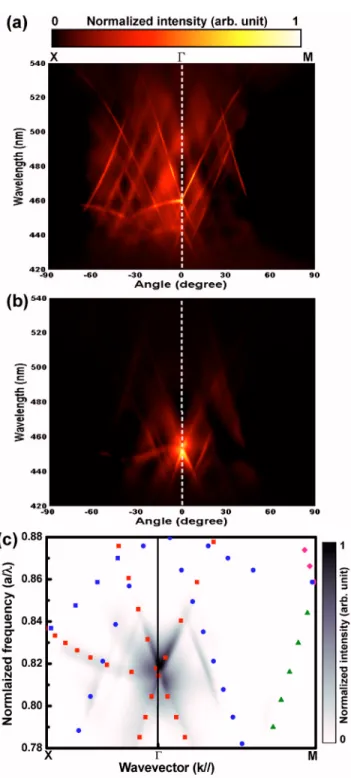
To increase the LEE and obtain a directional far-field emission pattern from a non-optimized cavity length of 550 nm GaN uMCLED, we used the GaN uMCLED incor-porated with a PhC lattice to enhance the LEE. Angular-spectra-resolved EL measurement indicated GaN PhC uMCLED with a square PhC lattice constant of a = 370 nm, and two different PhC hole depths, where the shallow and deep etching of the PhC hole depth were about 100 and 250 nm. This is clearly shown in Figs. 3共a兲 and 3共b兲 with light collected along the⌫X 共left兲 and ⌫M 共right兲. The shape of MQW line normalized these angular spectra of GaN PhC uMCLED. The light traveling through the waveguide in the GaN PhC uMCLEDs was diffracted by reciprocal wave vec-tors associated with the PhC. The sharp lines could be attrib-uted to extracted wave guided modes propagating in the GaN waveguides formed with the GaN ultrathin cavity between the Ag reflector mirror and the air. Observations of the GaN shallow-PhC uMCLEDs revealed only two lower-order guided mode extractions, as shown in Fig. 3共a兲. In contrast, Fig.3共b兲 illustrated the GaN deep-PhC uMCLEDs in nearly single guided mode extraction. To study these modes more clearly, this study transformed the spectra shown in Fig.3共b兲 to the guided mode dispersion curves shown in Fig.3共c兲. The image shows the normalized dispersion curves for each mode line in the⌫X 共left兲 and ⌫M 共right兲 directions, which were sections of the band of PhC. They can be quantitatively analyzed using the Ewald construction of the Bragg diffrac-tion theory in reciprocal space.8When the in-plane compo-nent of the resultant wave vector after coupling to a recipro-cal lattice vector fell within the circle of air, the diffracted
light escaped into the air. To study the observed lines of guided mode, the dispersion of the effective refractive index
nm,eff共兲 of fundamental mode 共m=0兲 was calculated by a
slab waveguide with the GaN material dispersion formula as a Sellimer equation.7 The effective refractive index disper-sion curves of the fundamental mode were calculated by a Bragg diffraction equation as 兩k0,eff⫾xG兩⬍k0, where k0,eff
= 2n0,eff共兲/ is a wave vector of the fundamental mode effective refractive index dispersion; ko= 2/o is a wave vector of the air circle; x = 1 , 2 , . . . is an integer of diffraction
FIG. 2.共Color online兲 Normalized EL angular spectra of the GaN non-PhC uMCLED for the resonant 550 nm cavity device.
FIG. 3.共Color online兲 Un-polarized angular-spectra-resolved measurements of the GaN PhC uMCLED with PhC hole depths共a兲 shallow t=100 nm and 共b兲 deep t=250 nm of the PhC lattice constant a=370 nm, where ⌫X is 共left兲 and ⌫M is the 共right兲 direction. 共c兲 shows the guided mode dispersion curves determined from the data shown in共b兲 and compared with the fun-damental mode effective refractive index dispersion curves for the trans-verse electric共TE兲 modes.
013108-2 Lai et al. Appl. Phys. Lett. 97, 013108共2010兲
This article is copyrighted as indicated in the article. Reuse of AIP content is subject to the terms at: http://scitation.aip.org/termsconditions. Downloaded to IP: 140.113.38.11 On: Wed, 30 Apr 2014 10:06:19
order; 2G⌫X共square, 䊏兲, GX1M共circle, 쎲兲, G⌫M共triangular, 䉱兲, and 2G⌫M 共rhombus, ⽧兲 of four reciprocal diffraction vector interactions with ⌫X and ⌫M direction of the square PhC lattice,8as shown in Fig.3共c兲. These dispersion curves were used to match the observing guided mode lines in Fig.
3共c兲. The fundamental guided mode was clearly visible and could be matched to the corresponding fundamental mode effective refractive index dispersion curves. This indicated that the measured guided mode was accurate. In addition, this study proved the guided mode dispersion of Fig. 3共a兲 agreed with the first 共m=0兲 and second 共m=1兲 lower-order guided mode effective refractive index dispersion curves. The above results revealed the near single guided mode ex-traction of Fig. 3共c兲, because 2G⌫X had interacted with the second-order guided mode appearing in Fig. 3共c兲 关observed
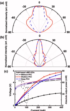
from Fig. 3共a兲兴. Results for guided mode dispersion were different from previous work with shallow PhC etching of GaN PhC MCLEDs, where the dispersion was simply that of folded free-photon bands.2,3 In addition, the other higher-order modes are not extracted. The reason for the mismatch between samples is due to the tilting during the lapping and polishing or reabsorption in the MQW as well as absorption in doped or metallic layers influenced the extracted modes.4 To investigate how the depth of the PhC hole t influ-enced the distribution of far-field emission distribution of GaN PhC uMCLED, this study measured the 3D far-field radiation pattern of GaN uMCLED, with and without the PhC structure, by means of imaging spheres共Radiant imag-ing IS-LI兲 under the same current 共50 mA兲 for beam shape comparison, normalized with peak intensity, as shown in Figs. 4共a兲 and 4共b兲. The measured far-field pattern at half intensity of the GaN non-PhC uMCLED was 104.17° that is much lower than that of the typical Lambertian cone 120° due to strong influence of the microcavity.6 The shallow 共⬃100 nm兲 and deep 共⬃250 nm兲 PhC hole depth t of the GaN PhC uMCLEDs caused differing far-field emission pat-terns, as shown in Figs. 4共a兲and4共b兲. The patterns peaked near normal on the surface of the device with far-field angle 共at half intensity兲 of 120.54° 共84.88°兲 and 30.75° 共34.38°兲 in ⌫X and 共⌫M兲, respectively. The GaN deep-PhC uMCLEDs based on near single lower-order guided modes and the strong influence of microcavity caused a highly-directional far-field emission pattern. Therefore, the depth of the PhC hole t and GaN cavity thickness T that affected the guided modes extraction behavior, had significantly modified the distribution of the directional far-field emission on GaN PhC uMCLED.
We measured the characteristics of the absolute light output power-current-voltage 共L-I-V兲 using an integration sphere with a back-illuminated charge coupled device共CCD兲 detector 共CAS 140CT—the standard for array spectrom-eters兲. The turn-on voltage of the devices was 2.8 V. The forward voltage of GaN uMCLED with and without PhC was 4.62 V and 4.4 V, respectively, under the current 350 mA, as shown in Fig.4共c兲. The absolute light output power of the GaN deep-PhC uMCLED under the driven current of 350 mA shows efficiency of the output power enhanced by 145.9% 共⬃2.46⫻兲, compared with the GaN non-PhC uMCLED as shown in Fig. 4共c兲. GaN deep-PhC uMCLED exhibited a highly-directional light enhancement, compared
with the GaN non-PhC uMCLED with the same cavity thick-ness.
In conclusion, this study conducted experiments and a theoretical investigation into directional far-field emission patterns based on the influence of microcavity and near single guided mode extraction of GaN PhC uMCLEDs. Angular-spectra-resolved EL measurements showed a corre-lation between photon-band structure and guided mode ef-fective refractive index dispersion curves. The GaN deep-PhC uMCLED showed highly-directional far-field emission patterns at half intensity near ⫾15°. The results indicated that highly-directional far-field light extraction efficiency could contribute to the development of many applications, especially for limited etendue applications such as pico-projectors.
1M. R. Krames, O. B. Shchekin, R. Mueller-Mach, G. O. Mueller, L. Zhou, G. Harbers, and M. G. Craford,J. Disp. Technol. 3, 160共2007兲.
2C. F. Lai, C. H. Chao, H. C. Kuo, H. H. Yen, C. E. Lee, and W. Y. Yeh,
Appl. Phys. Lett. 94, 123106共2009兲.
3K. Bergenek, C. Wiesmann, H. Zul, C. Rumbolz, R. Wirth, N. Linder, K. Streubel, and T. F. Krauss,IEEE J. Quantum Electron. 45, 1517共2009兲.
4J. J. Wierer, A. David, and M. M. Megens,Nat. Photonics 3, 163共2009兲. 5Y. S. Choi, M. Iza, E. Matioli, G. Koblmuller, J. S. Speck, C. Weisbuch,
and E. L. Hu,Proc. SPIE 6910, 69100R共2008兲.
6P. M. Pattison, A. David, R. Sharma, C. Weisbuch, S. DenBaars, and S. Nakamura,Appl. Phys. Lett. 90, 031111共2007兲.
7M. Bass, Devices, Measurements, and Properties, 2nd ed., Handbook of Optics Vol. 2共McGraw-Hill, New York, 1995兲.
8C. F. Lai, J. Y. Chi, H. C. Kuo, H. H. Yen, C. E. Lee, C. H. Chao, W. Y. Teh, and T. C. Lu,IEEE J. Sel. Top. Quantum Electron. 15, 1234共2009兲.
FIG. 4. 共Color online兲 The far-field emission pattern shows the PhC lattice constant a = 370 with different hole depth 共a兲 shallow t=100 nm and 共b兲 deep t = 250 nm of GaN PhC uMCLED, where the solid line indicates the direction of the⌫X and the dash line indicates the direction of ⌫M. 共c兲 The characteristics of absolute light output power-current-voltage共L-I-V curves兲 of the GaN uMCLEDs with and without PhC.
013108-3 Lai et al. Appl. Phys. Lett. 97, 013108共2010兲
This article is copyrighted as indicated in the article. Reuse of AIP content is subject to the terms at: http://scitation.aip.org/termsconditions. Downloaded to IP: 140.113.38.11 On: Wed, 30 Apr 2014 10:06:19