國
立
交
通
大
學
電機學院微電子奈米科技產業研發碩士專班
碩
士
論
文
低溫下利用大氣電漿沉積二氧化矽薄膜作為有機薄膜電晶
體之閘極絕緣層在不同基本製程參數之研究
Investigation of the thin silicon oxide deposited with different
basic process parameters of atmospheric-pressure plasma jet at
low temperature for OTFTs Gate insulator
研
究
生:蔡 堃 濠
指導教授:張 國 明 教授
低溫下利用大氣電漿沉積二氧化矽薄膜作為有機薄膜電晶體之閘
極絕緣層在不同基本製程參數之研究
Investigation of the thin silicon oxide deposited with different basic
process parameters of atmospheric-pressure plasma jet at low
temperature for OTFTs Gate insulator
學生:蔡堃濠 Student:Kun-Hao Tsai
指導教授:張國明 博士 Advisor:Dr. Kow-Ming Chang
國 立 交 通 大 學
電機學院微電子奈米科技產業研發碩士班 碩 士 論 文
A Thesis
Submitted to College of Electrical and Computer Engineering National Chiao Tung University
in partial Fulfillment of the Requirements for the Degree of
Master In
Industrial Technology R & D Master Program on Microelectronics and Nano Sciences
January 2009
低溫下利用大氣電漿沉積二氧化矽薄膜作為有機薄
膜電晶體之閘極絕緣層在不同基本製程參數之研究
學生:蔡堃濠
指導教授:張國明 博士
國立交通大學電機學院產業研發碩士班
摘要
我們成功地在低製程溫度下製作低操作電壓頂部接觸之汲極
與源極結構的有機薄膜電晶體,且利用大氣電漿技術在基板溫
150℃和大氣壓下成長閘極介電層,在這樣的製程環境可以改善大
面積的製程能力以利於應用在顯示器上並且減少設備的費用,我
們發現大氣電漿沉積的矽氧化物的品質強烈取決於主要氣體、設
備的電漿噴嘴和表面之間的距離與氬氣的流量,而這些因素甚至
也影響沉積速率。我們藉由改善閘極絕緣層的特性可使得有機薄
膜電晶體可以得到良好的電性,其載子遷移率達到 0.66 cm
2/
V‧s、操作電壓約在-2 V、次臨界擺幅約 0.7 V/dec。
Investigation of the thin silicon oxide deposited with different
basic process parameters of atmospheric-pressure plasma jet
at low temperature for OTFTs Gate insulator
Student:Kun-Hao Tsai Advisor:Dr. Kow-Ming Chang
Industrial Technology R & D Master Program of
Electrical and Computer Engineering College
National Chiao Tung University
ABSTRACT
Low operation voltage organic thin film transistors (OTFTs) were successfully fabricated with top contact structure at low fabrication temperature. The thin gate dielectric of OTFTs were deposited by atmospheric pressure plasma jet at the substrate temperature about 150
℃
and under atmospheric pressure. The environment of processes would significantly improve the abilities of large area application for display and decrease the cost of instruments. We found that the quality of silicon oxide deposited by atmospheric pressure plasma jet strongly depended on the main gas, the gap distance between plasma nozzle and surface of the device, and the Ar flow rate even influenced the deposition rate. Due to the誌謝
首先,要感謝的是我的指導老師張國明教授,在這兩年的碩士
研究生涯裡給予熱心的指導和教誨,使的我不論在研究上或待人
處事上都有很大的收穫,更給我們建立獨立思考解決問題的觀
念,在此獻上我最深的謝意。
再來,我要感謝菘宏學長及知天學長的建議及協助,謝謝各
位學長在研究上所提供的意見和幫助,讓我增廣不少專業領域的
知識,此外也要感謝士軒學長對我的教導和鼓勵,讓我得以順利
完成實驗並順利的完成碩士學業。
接下來我還要感謝的是一起陪我瘋狂做實驗的彥凱同學,度
過了許多無聊的等待時間。還有天佑與育彬,有了各位,才讓我
的研究生活充滿歡樂與色彩,很高興與各位度過這美好的時光,
做實驗有你們的相伴,讓我倍感溫馨,感謝大家的鼓勵與支持謝
謝你們。
最後,我要感謝我的父母與兄弟姊妹給了我最大的支持和鼓
勵,因為有你們溫馨的關懷,讓我覺得一切都過的很豐富,有了
你們的支持與栽培,才有今日順利完成自己的理想,讓我能順利
完成學業,我相信他們會以我為榮。
Contents
Chinese Abstract
………..………..………iEnglish Abstract
………....iiAcknowledgement (in Chinese)
...iiiContents
……….…...………...…………....ivTable Captions
………..………...………...viFigure Captions
……….………...……….…….viiiChapter 1 Introduction
………..………..……….……….……11.1 History of OTFT and motivation
…..…..…….…………11.2 Introduction of OTFT
…..………...……….………..21.2.1 Introduction of organic semiconductor
……….….….21.2.2 Pattern of active region….
……….…………31.2.3 High dielectric constant insulator
….………….….………..41.2.4 Source/Drain contact
…..………..……….….……….5
1.2.5 The structure of organic TFT
………….………..………….61.3 Introduction of pentacene and fabrication
method
……….……….61.4 Thesis Organization
……….…………...……….72.2 Affect to capacitance of different conditions
…..…182.2.1 Silicon oxide deposited by APPJ on the metal insulator
metal(MIM) structure and relation with main gas of
APPJ
………..…...……….182.2.2 Silicon oxide deposited by APPJ on the metal insulator
metal (MIM) structure and relation with gap distance of
APPJ
………....………....………...…...……….192.2.3 Silicon oxide deposited by APPJ on the metal insulator
metal (MIM) structure and relation with Ar flow rate of
APPJ
……….…………..……..…….202.3 Fabrication of OTFT
……….…….….………… .212.4 Characteristic measurement of devices
…… ….…...22Chapter 3 Results and Discussion
...313.1 Result of different conditions
……….…….….……313.1.1 The influence of different main gases
…………..……….313.1.2 The influence of different gap distances
………….…...333.1.3 The influence of different Ar flow rates
………..….343.2 OTFT electric characteristics discussion
……….….35Chapter 4 Conclusions and Future work
...514.1 Conclusions
…...514.2 Future work
………...……….………52Table Captions
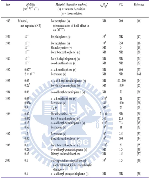
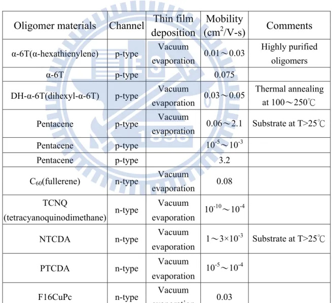
Table 1-1 Highest field-effect mobility(μ) values measured from OTFT as eported in the literature annually from 1986 through 2000……….….9 Table 1-2 Characterization of materials for OTFT………..………..10 Table 1-3 Thin film transistor performances for different oligomer active
layers………..…12 Table 2-1 Densities of oxygen species in the various plasma discharges…..……25 Table 2-2 shows the detail experimental parameters of silicon oxide deposited with different kinds of main gases……….………26 Table 2-3 shows the detail experimental parameters of silicon oxide deposited with different kinds of gap distances….……….……….…...28 Table 2-4 shows the detail experimental parameters of silicon oxide deposited with different kinds of Ar flow rates.………..………...28 Table 3-1 shows the deposition rate and thickness of silicon oxide deposited with different main gases of atmospheric pressure plasma jet………..…….37 Table 3-2 shows the leakage current density (A/cm2 ) at 0.5 and 1 MV/cm with different main gases….……….……….38 Table 3-3 Densities of oxygen species in the plasma discharges………..……….38 Table 3-4X-ray photoelectron spectroscopy analysis the silicon oxide with different main gases of atmospheric pressure plasma jet……..……...41 Table 3-5 shows the deposition rate and thickness of silicon oxide deposited with different gap distances of atmospheric pressure plasma jet……..…….42
Table 3-7 shows the deposition rate and thickness of silicon oxide deposited with different Ar flow rates of atmospheric pressure plasma jet………...…44. Table 3-8 shows the leakage current density (A/cm2 ) at 0.5 and 1 MV/cm with different Ar flow rates………..………..…45
Figure Caption
Figure 1-1 Semilogarithmic plot of the highest field-effect mobility(μ) Reported for OTFT fabricated from the most promising polymeric and
oligomeric semiconductors versus year from 1986 to 2000…...……..8. Figure 1-2 Classification of semiconductor materials……..……….10 Figure 1-3 (a) Cross section view of top contact structure of OTFT
(b) Cross section view of bottom contact structure of OTFT…..……11 Figure 1-4 Molecular structure of pentacene………..………...12 Figure 2-1 Schematic of a corona discharge………..………23 Figure 2-2 Schematic of a silent discharge (1) metallic electrodes and
(2) dielectric barrier coating…….…..23 Figure 2-3 Schematic of a cold plasma torch (m.b. = matchbox)………..………23 Figure 2-4 Schematic of the atmospheric-pressure plasma jet for the deposition of silica films………..……..24 Figure 2-5. Numerical simulation of the concentrations of species in the effluent of the plasma jet as a function of the distance from the nozzle in a 1.0% O2 /He plasma at 760 torr………24 Figure 2-6 APPJ system of ITRI……….………….……..25 Figure 2-7 Schematic of the atmospheric-pressure plasma jet for the deposition of silicon oxide………..……...26 Figure 2-8 The MIM structure of different APPJ parameters…………..………..27
Figure 3-2 SEM images of silicon oxide fabricated with different main gases of atmospheric pressure plasma jet. (a) CDA (b) N2 (c) O2……...…39 Figure 3-3 AFM images of silicon oxide fabricated with different main gases of atmospheric pressure plasma jet.(a) CDA (b) N2 (c) O2…..……..40 Figure 3-4 Deposited rate and RMS of silicon oxide deposited with different kinds of main gases of atmospheric pressure plasma jet………..………….41 Figure 3-5 Electric field versus leakage current density of silicon oxide with different gap distances of atmospheric pressure plasma jet……….…42 Figure 3-6 Deposited rate and RMS of silicon oxide deposited with different kinds gap distances of atmospheric pressure plasma jet……….….….…...43 Figure 3-7. Electric field versus leakage current density of silicon oxide with different Ar flow rates of atmospheric pressure plasma jet…..…..…..44 Figure 3-8. SEM images of silicon oxide fabricated with different Ar flow rates of atmospheric pressure plasma jet. (a) 60sccm (b) 100sccm (c) 140sccm (d) 200sccm (e) 300sccm………..…………..…..46 Figure 3-9 AFM images of silicon oxide fabricated with different Ar flow rates of atmospheric pressure plasma jet. (a) 60sccm (b) 100sccm (c) 140sccm (d) 200sccm (e) 300sccm………..…..…………..47 Figure 3-10 Deposited rate and RMS of silicon oxide deposited with different kinds of Ar flow rates of atmospheric pressure plasma jet…………49 Figure 3-11 Transfer characteristics IDS -VG and (-IDS)1/2 - VG of OTFT.... …...….49
Figure 3-12 Output characteristics of the penecene-based OTFTs with silicon oxide deposited with atmospheric pressure plasma jet………...…...50
Chapter 1
Introduction
1.1
History of OTFT and motivation
More and more studies of organic thin film transistor are proposed in recent years because of its attracting applications. OTFTs could be applied for flexible displays and electronic circuit such as e-paper, smart card, and radio-frequency identification (RF-ID)[1]-[3] requiring low temperature processes and low overall cost. In the semiconductor industry equipment front end of the line, main consist of the Chemical Vapor Deposition, Implant, etch, Chemical mechanical Polishing, process control, and so on , The formation methods of gate dielectric were widely studied such as sol-gel, PECVD, sputter, anodic oxidation [4]-[8], and so on. However, PECVD, implant,etch and sputter must be operated in a vacuum chamber which is not suitable for large area applications. Although sol-gel method could utilize spin coater to fabricate insulator, it usually needs a long time to anneal. In order to overcome the large operation voltage of OTFTs, the high dielectric constant material must be introduced into gate oxide of OTFTs to enhance the field-induced carrier density and reduce leakage current. There are various gate dielectric materials which have been investigated and published for OTFTs such as TiO2, Si3N4, Ta2O5 [4],[6],[8],[9]. In this paper, we have selected thin silicon oxide as the gate dielectric because it has larger band gap about 8.9 ev for suppressing the gate leakage current. The operation voltage would affect the power
In the past the atmospheric pressure plasma jet was usually used to apply for surface treatment and cleaning [11]. In this study, the atmospheric pressure plasma jet was used to deposit gate insulator of OTFTs. Atmospheric pressure plasma jet, operating at atmospheric pressure, could overcome the limitation of substrate size. Moreover, the temperature of plasma jet processes could be below 150 , being suitable ℃ for plastic substrate [11].
1.2 Introduction of OTFT
1.2.1 Introduction of organic semiconductor
The molecules of the organic semiconductor are joined to by van der Waals power with energy smaller than 10 kcal mol-1. This weak interaction energy of molecules may take responsibility for the low upper limit of carrier motilities, falls between 1-10 ㎝² / Vs by time-of-flight measurement [12], due to the energy of vibrations of the molecule is close to this value. Interaction energy of molecules of inorganic semiconductors is strong such as 76 kcal mol-1 in silicon. Thus the carriers move as highly delocalized plane waves in wide band with high mobility.The semiconducting materials generally divide into the organic materials with the inorganic materials. Inorganic, atoms are bonded by strong covalent bond, result as the higher carrier mobility.
Organic semiconductor materials such as polythiophene, poly (3-hexylthiophene) (P3HT) have been investigated for use in field effect transistors [13]. We presented a semilogarithmic plot of the highest yearly reported field-effect mobility value measured from thin-film transistors based on specific organic semiconductors, beginning in 1986. An update of that plot is shown in Figure 1-1 and, which is based on Table 1-1 [14].
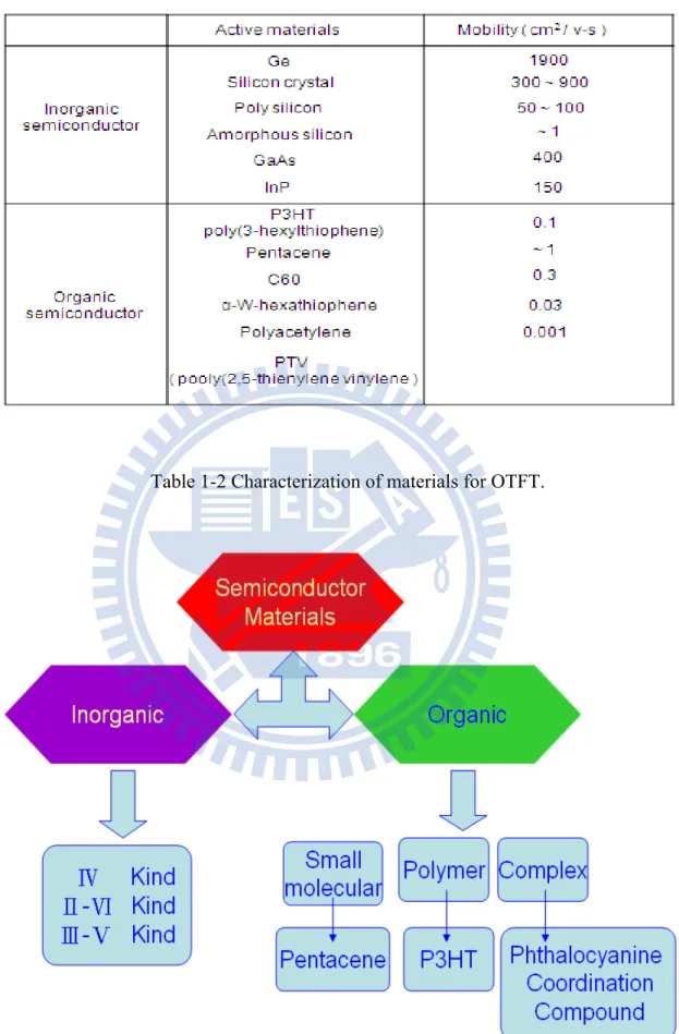
Organic, molecules are bonded by weak Van der Waal forces. Lower mobility is due to the localized-states carriers. View Table 1-2. The inorganic semiconductor materials usually use have several kinds. View Figure 1-2.
The small molecular material usually uses evaporative process, therefore, it needs the perfect vacuum the environment. Making the manufacture process to be relatively complex moreover the cost also relatively to enhance. N-type of the small molecular material carries transmission characteristic poorly. The material appears extremely does not stabilize in the air environment. But also has one kind of semiconducting organic material to be called a-nT(Ol igothiophene) . Researches and develops the improvement material the stability to be good and the characteristic nice in the air environment . P-type of the small molecular material most has the representative material is pentacene..Among all semiconducting organic materials used to fabricate OTFT, pentacene is the most popularly used organic material to serve as the active layer because of its higher carrier mobility in OTFTs .
1.2.2 Pattern of active region
In order to obtains the high efficiency the experiment,develops many conveniences process technology, a variety of strategies have been used to create integrated arrays of transistors including photolithography, stamping, and shadow masking, photolithography has an established in frastructure thanks to its extensive use in silicon fabrication ,printing process in which the printing surface is neither raised no retched into the plate , and printing is affected by means of a chemical process that allows ink to adhere to only the parts of the surface to be reproduced . Photolithographic patterning
1.2.3 High dielectric constant insulator
The effect of flexible electronic products for human life will grow drastically in the near future. A reliable low temperature process becomes more and more important and urgent for OTFT fabrication since a critical issue in OTFT fabrication is that the flexible substrate cannot suffer high temperature. There are some low temperature methods used to fabricate inorganic gate insulator reported in many studies such like sol-gel, PECVD,sputter, and anodic oxidation [4-8]. Although the dielectric could be deposited or grown at low temperature,however, in order to reduce gate leakage current for obtaining a good gate dielectric property, a high temperature annealing after dielectric deposited is needed. Besides, a good gate insulator with high dielectric constant at low-temperature process is urgently demanded for the portable application on OTFT now. A low operation voltage for OTFT is required to reduce power consumption from flexible electronic circuits. By adopting some high dielectric constant materials such as Al2O3 [15] and HfO2 [16] for OTFT are a common way to reduce the operation voltage. Increase dielectric constant with reduce leakage current for OTFT, phenomenon of leakage current involve defect density and charge trap density at low temperature process,charge trapped in defects causes a shift in the gate threshold voltage of the OTFT, the trapped charge will change with change with time so the threshold voltage will shift with time, leading to instability of operating characteristics, and occur increase scatter carriers so that low mobility for OTFT performance, hence, influence of dielectric quality is important for OTFT research.
1.2.4 Source/Drain contact
The position of the Fermi level is a quite important consideration in the semiconductor. As a result of metallic work function consideration, whether forms barrier or ohmic contact interface between metal and semiconductor. and it is decided to the fermi level position.Therewith judges fermi level the relative position to decide type of conduction condition . If semiconduct or fermi level approaches valence band, treatsas by the hole carries to convey. Therefore is called the p-type semiconductor. Adversative , if semiconductor fermi level approaches conduction band, treats as by the electron carries to convey.Therefore i s called the n-type semiconductor. Consequently, we will improve interface to avoid forming Schottky barrier and creates oversized contact resistance to affect the device characteristics .
For example, a transmission line study of contact resistances in pentacene TFTs has been published by Jackson [17] and it shows significant differences in the contact properties for top versus bottom contact devices. In a more previous research, Dimitrakopoulos and co-workers demonstrated that for bottom contact TFTs there is a region of disorder in the pentacene thin near the contact interface, though the disorder can be mitigated by thiolating the contacts [18].It is a straightforward method to find a suitable electrode material which forms ohmic contact with the organic active layer and thus to improve the performance of OTFT. Pentacene can form an ohmic contact with material for its work function larger than 5.1eV because the work function of pentacene is 5.1eV. Work functions of all materials we used are larger than 5.1eV; they include Ni (5.1eV), Pt (5.65eV), Cr (4.5eV).
1.2.5 The structure of organic TFT
Figure 1-3 show the standard two kind of organic TFTs configuration, (a) is the inverted staggered type TFT and (b) is the inverted coplanar type TFT. Usually, the former is also called the top contact and the latter is called the bottom contact TFT.
1.3 Introduction of pentacene and fabrication method
Pentacene (from penta = five, and acenes = polycyclic aromatichydrocarbons with fused benzene rings) is a fused-ring polycyclicaromatic hydrocarbon. Structure of pentacene is shown in Figure 1-4.The lattice parameters of Structure of pentacene are shown in Table 1-3. And the other important parameters are descry bed as follows: [19,20]Pentacene Formula: C22H14 ; Molecular weight: 278.3 ; Melting point:573K ; Volume of the unit cell: 705.0°Å³ ; Density:1.303g.cm-3(calculated with Z = 2), 1.30 g.cm-3(measured) ; OpticalBandgap: 2.8eV ; Absorption coefficient for X-rays: λ = 1.542nm ;Resistivity: ~1014-1015 ohm-cm;
On organic small molecules, the highest hole and electron mobility has been demonstrated by pentacene(C22H14). Pentacene has a strong inclination to form molecular crystals and when deposited by evaporation will typically form well-ordered films even for low substrate temperatures. For example, pentacene is deposited by evaporation at room temperatures can be obtained ordered films. For organic semiconductor, the well-ordered films are extremely important.
A more promising process to realize large area electronics is the thermal evaporation of organic material. The thermal evaporated material is poly crystalline with large grain sizes, usually in the range of a few microns. The mobility of polycrystalline transistors at room temperature can achieve the same range as amorphous silicon, is about 0.1-1 ㎝² / Vs.
1.4 Thesis Organization
In our work, the TEOS films that are deposited by atmospheric-pressure plasma jet technology (APPJ) as gate dielectric layers of OTFT. Then pentacene films are deposited by a thermal evaporation system as active layers in OTFT. Last we will discuss the influence.
In chapter 1, we describe history of OTFT and motivation of our study.And we introduce to organic semiconductor and structure.
In chapter 2, we will introduce a new process, APPJ, which can be operated under low temperature and atmospheric ambient. And APPJ will make use of deposit dielectric layer SiO2 for our experiment.
In chapter 3, we compare the various methods of MIM fabrication and we select the best parameter to fabricate OTFT. Last we discuss the results.
Figure 1-1 Semilogarithmic plot of the highest field-effect mobility(μ) Reported for OTFT fabricated from the most promising polymeric and oligomeric semiconductors versus year from 1986 to 2000[16].
Table 1-2 Characterization of materials for OTFT.
Figure 1-4 Molecular structure of pentacene.
Oligomer materials Channel
Thin film Mobility
(cm
2/V-s)
Comments
deposition
α-6T(α-hexathienylene) p-type Vacuum 0.01~0.03 Highly purified
evaporation oligomers
α-6T p-type 0.075
DH-α-6T(dihexyl-α-6T) p-type Vacuum 0.03~0.05 Thermal annealing
evaporation at 100~250℃
Pentacene p-type Vacuum 0.06~2.1 Substrate at T>25℃ evaporation Pentacene p-type 10-5~10-3 Pentacene p-type 3.2 C60(fullerene) n-type Vacuum 0.08 evaporation TCNQ n-type Vacuum 10-10~10-4 (tetracyanoquinodimethane) evaporation
NTCDA n-type Vacuum 1~3×10⁻³ Substrate at T>25℃ evaporation
PTCDA n-type Vacuum 10-5~10-4
evaporation
F16CuPc n-type Vacuum 0.03
evaporation
Chapter 2
Experiment
2.1 Introduction of APPT
2.1.1 Introduction of plasma[21]
(a)
Corona discharge
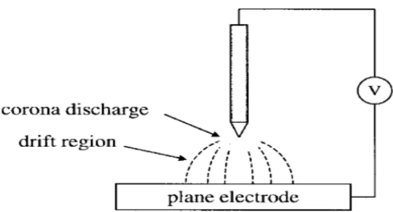
.A corona discharge appears as a luminous glow localized in space around a point tip in a highly nonuniform electric field. The physics of this source is well understood . The corona may be considered a Townsend discharge or a negative glow discharge depending upon the field and potential distribution . Figure 2-1 shows a schematic of a point-to-plane corona. The apparatus consists of a metal tip, with a radius of about 3μm, and a planar electrode separated from the tip by a distance of 4–16 mm . The plasma usually exists in a region of the gas extending about 0.5 mm out from the metal point. In the drift region outside this volume, charged species diffuse toward the planar electrode and are collected. The restricted area of the corona discharge has limited its applications in materials processing. In an attempt to overcome this problem, two-dimensional arrays of electrodes have been developed. Some applications of coronas include the activation of polymer surfaces and the enhancement of SiO2 growth during the thermal oxidation of silicon wafers.
order of several mm, and the applied voltage is about 20 kV. The plasma is generated through a succession of micro arcs, lasting for 10–100 ns, and randomly distributed in space and time. These streamers are believed to be 100μ m in diameter and are separated from each other by as much as 2 cm . Dielectric barrier discharges are sometimes confused with coronas, because the latter sources may also exhibit microarcing. Dielectric barrier discharges have been examined for several material processes, including the cleaning of metal surfaces and the plasma-assisted chemical vapor deposition of polymers and glass films . However, since the plasma is not uniform, its use in etching and deposition is limited to cases where the surface need not be smooth. For example, in the study of SiO2 deposition, it was found that the surface roughness exceeded 10% of the film thickness.
(c)Cold plasma torch
A “cold” plasma torch was first described by Koinuma et al. in 1992. A schematic of this source is shown in Figure 2-3. The powered electrode consists of a metal needle with a thickness of 1 mm. This needle is inserted into a grounded metal cylinder. In addition, a quartz tube is placed between the cathode and anode, which makes this device resemble a dielectric barrier discharge. Mixtures of rare gases, He and Ar, and other species are fed between the metal needle and quartz tube at flow velocities of about 5 m/s at 200–400℃. The gases are ionized and exit the source as a small jet. Koinuma and coworkers have employed the cold plasma torch in a number of materials processes, including silicon etching , photoresist ashing , deposition of SiO2 , and TiO2 films , treatment of vulcanized rubber , and the production of fullerenes . Koinuma and coworkers measured the electron temperature in the plasma effluent with a Langmuir probe and found it to be between 1–2 eV depending on the gas composition.
(d) Plasma jet
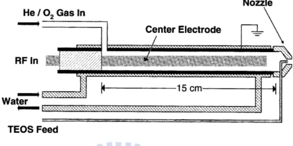
Shown in Figure 2-4 is a schematic of an atmospheric-pressure plasma jet . This new source consists of two concentric electrodes through which a mixture of helium, oxygen, and other gases flow. By applying 13.56 MHz RF power to the inner electrode at a voltage between 100–250 V, the gas discharge is ignited.
The ionized gas from the plasma jet exits through a nozzle, where it is directed onto a substrate a few millimeters downstream. Under typical operating conditions, the gas velocity is about 12 m/s with the effluent temperature near 150℃. So far, this source has been used to etch polyimide, tungsten, tantalum, and silicon dioxide , as well as to deposit silicon dioxide films by plasma-assisted chemical vapor deposition.
Langmuir probe measurements in the jet effluent indicate that the concentration of charged species is relatively low, on the order of 1 ×1010cm-3 . However, inside the jet the electron density should be much higher, as suggested by the intense atomic lines observed in the optical emission spectrum. Based on the impedance measurements and the emission spectra, it is estimated that the electron temperature inside the plasma jet averages between 1–2 eV.
Jeong et al. measured the ozone concentration in the effluent of the plasma jet at different distances from the nozzle and found that it varied from 2–5×1015 cm -3, as shown in Figure 2-5. Using these data as the basis for fixing the other species concentrations, a preliminary kinetic model was developed to determine the concentrations of O atoms and metastable oxygen molecules in the jet effluent. These results are also shown in the figure. The simulation predicts that the O atom
be the active species in polyimide etching and in the SiO2 CVD process .
Comparison of various plasma sources show in Table 2-1.We find the average densities of oxygen ions,oxygen atoms, and ozone in the different atmospheric -pressure plasma discharges. Since the dielectric barrier discharge operates as a series of transient microarcs, it is difficult toobtain time-averaged values for the reactive species. However, perusal of the literature suggests that the time averaged concentrations should be similar to those found in a corona. Also, the values shown for the plasma jet correspond to the gas in between the electrodes. In the downstream jet, the distribution of species changes as indicated in Figure 2-5.
In the corona and dielectric barrier discharge, ozone is the main reaction product, whereas in the other plasmas, oxygen atoms represent a large fraction of the reactive species. In a low-pressure glow discharge the concentrations of ions and atoms are lower than in an atmospheric-pressure plasma. However, the impingement rate of these species on a substrate may be about the same in both cases, since the flux to the surface increases with decreasing pressure. Taking into account all the properties of the plasmas, it appears that the atmospheric-pressure plasma jet exhibits the greatest similarity to a low-pressure glow discharge. Consequently, this device shows promise for being used in a number of materials applications that are now limited to vacuum.
2.1.2 Applications of APPJ
The atmospheric-pressure plasma jet technology (APPJ) is useful for treating and modifying the surface properties of organic and inorganic materials. The APPJ apparatus does not require any vacuum systems, produces high density plasma, and provides treatment of various substrates at low temperatures while operating open to the atmosphere. The plasma system has used for a wide variety of applications including treatment of polymer films, paper, wood, and foils; plasma grafting and plasma polymerization; ash various materials in the microelectronics industry; barrier layer deposition for the packaging industry; and sterilizing biologically contaminated materials.
For polymer films, the technique offers the following advantages: • Uniform treatment and No backside treatment.
• Improved surface energy with concomitant improved wet ability, printability,and adhesion.
• No additional vacuum system and low cost.
• Continuous fabrication availably and high speed for production. • High plasma density.
As shown in Fig.2-6, we exhibited the atmospheric-pressure plasma system which was used in our experiment.
2.2 Affect to capacitance of different conditions
2.2.1 Silicon oxide deposited by APPJ on the metal insulator
metal (MIM) structure and relation with main gas of
APPJ
In this section, we are resolution to deposit silicon oxide dielectric on the bottom contact electrode metal by atmospheric-pressure plasma jet with different main gas. But silicon oxide is not deposited on the metal at room temperature. Accordingly, we heat the bottom of n+-Si substrate and enable TEOS to be deposited on the metal.
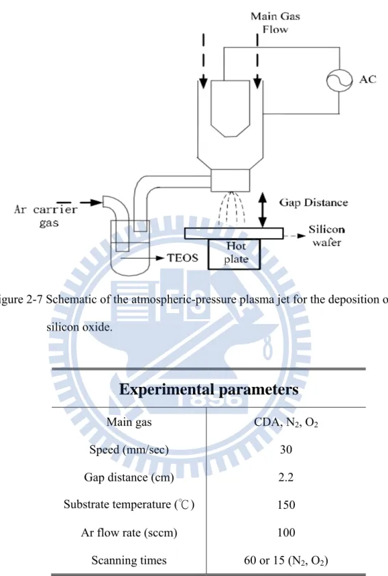
First, an n-type bare silicon wafer is cleaned by the standard RCA cleaning process. An insulating layer of silicon dioxide is grown by thermaloxidation (wet oxidation) 90min at 950 for isolation purpose. ℃ The thickness of silicon oxide is 5060 Å measured by n&k system. And deposited 50 nm Nickel as the bottom electrode. Heats up the Tetraethoxy silane (TEOS) to 150 was injected by Argon as carrier gases which is the ℃ deposition source of silicon oxide. Silicon oxide is deposited on the top of Nickel layer at room temperature under an atmospheric-pressure with the plasma power is established around 560 W with an appropriate scanning rate (cycle).Silicon oxide is deposited on the Nickel thin film by atmospheric-pressure plasma jet system (APPJ) was plot in Fig. 2.-7. with varied main gases (Qxygen, Nitrogen and CDA respectively). The detail experimental parameters show in Table 2-2. We adopt the experimental parameters to compare silicon oxide deposited with different main gases of APPJ.
Finally, all top contact electrodes are deposited 50 nm thick Nickel layer defined with shadow mask by E-Gun system. The active region pad of all capacitors is diameter 200μm. The process flow is shown in Figure 2.-8
2.2.2 Silicon oxide deposited by APPJ on the metal insulator
metal (MIM) structure and relation with gap distance of
APPJ
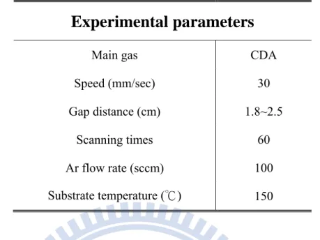
In this section, we are resolution to deposit silicon oxide dielectric on the bottom contact electrode metal by atmospheric-pressure plasma jet with different gap distance. But silicon oxide is not deposited on the metal at room temperature. Accordingly, we heat the bottom of n+-Si substrate and enable TEOS to be deposited on the metal. First, an n-type bare silicon wafer is cleaned by the standard RCA cleaning process. An insulating layer of silicon dioxide is grown by thermaloxidation (wet oxidation) 90min at 950 for isolation purpose. The thickness of silicon oxide is 5060 Å measured by ℃ n&k system. And deposited 50 nm Nickel as the bottom electrode. Heats up the Tetraethoxy silane (TEOS) to 150 was injected by Argon as carrier gases which is the ℃ deposition source of silicon oxide. Silicon oxide is deposited on the top of Nickel layer at room temperature under an atmospheric-pressure with the plasma power is established around 560 W with an appropriate scanning rate (cycle).Silicon oxide is deposited on the Nickel thin film by atmospheric-pressure plasma jet system (APPJ) with varied gap distances (1.8 cm, 2.0 cm, 2.2 cm and 2.5 cm respectively). The detail experimental parameters show in Table 2-3. We adopt the experimental parameters to compare silicon oxide deposited with different gap distances of APPJ.
Finally, all top contact electrodes are deposited 50 nm thick Nickel layer defined with shadow mask by E-Gun system. The active region pad of all capacitors is diameter
2.2.3 Silicon oxide deposited by APPJ on the metal insulator
metal (MIM) structure and relation with Ar flow rate of
APPJ
In this section, we are resolution to deposit silicon oxide dielectric on the bottom contact electrode metal by atmospheric-pressure plasma jet with different gap distance. But silicon oxide is not deposited on the metal at room temperature. Accordingly, we heat the bottom of n+-Si substrate and enable TEOS to be deposited on the metal.
First, an n-type bare silicon wafer is cleaned by the standard RCA cleaning process. An insulating layer of silicon dioxide is grown by thermaloxidation (wet oxidation) 90min at 950 for isolation purpose. The thickness of silicon oxide is 5060 Å measured by ℃ n&k system. And deposited 50 nm Nickel as the bottom electrode. Heats up the Tetraethoxy silane (TEOS) to 150 was injected by Argon as carrier gases which is the ℃ deposition source of silicon oxide. Silicon oxide is deposited on the top of Nickel layer at room temperature under an atmospheric-pressure with the plasma power is established around 560 W with an appropriate scanning rate (cycle).Silicon oxide is deposited on the Nickel thin film by atmospheric-pressure plasma jet system (APPJ) with varied Ar flow rates (60sccm, 100sccm, 140sccm, 200sccm and 300sccm respectively). The detail experimental parameters show in Table 2-4. We adopt the experimental parameters to compare silicon oxide deposited with different Ar flow rates of APPJ.
Finally, all top contact electrodes are deposited 50 nm thick Nickel layer defined with shadow mask by E-Gun system. The active region pad of all capacitors is diameter 200μm.
2.3 Fabrication of OTFT
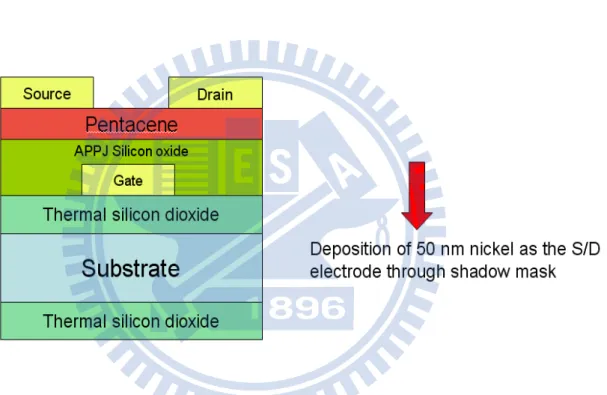
First, the n+-Si wafer was used as the substrate, and was rinsed in the deionization water ( DI water ), and was then dipped in dilute HF solution ( HF:DI water = 1:100 ) that to remove the native oxide, the wafer was accomplished the RCA Clean process. An insulating layer of silicon dioxide is grown by thermal oxidation (wet oxidation) 90min at 950 for isolation purpose. The thickness of silicon dioxide is 5060 Å ℃ measured by n&k system. A 50-nm-thick Nickel gate electrode was then deposited on SiO2/Si, through a shadow mask, using E-Gun. The thin silicon oxide gate dielectric was then deposited by atmospheric pressure plasma jet (APPJ) at substrate temperature of 150 in atmosphere ℃ . We used the Ar as the carrier gas to transport the TEOS vapor into the spray nozzle and the clean dry air (CDA) plasma to decompose the TEOS gas. The atmospheric pressure plasma jet has operation power about 560 W and the diameter of the plasma nozzle was about 5 mm.
After completing the deposition of gate dielectric, a 50 nm-thick pentacene active layer was evaporated on the gate insulator through a shadow mask in high vacuum about 2 x10⁻⁶ toor and the temperature was about 70 . The source and drain electrodes ℃ were then deposited on the surface of pentacene through shadow mask with a channel width W of 2000 μm and channel length L of 500 μm. The schematic diagram of OTFT with top contact structure was shown in Fig. 2-10.
2.4 Characteristic measurement of devices
We use HP 4284A precision LCR meter parameter to analyze Capacitance-Voltage (C-V) characteristic diagrams at 1MHz and the characteristic curves of Current-Voltage (I-V) are measured with semiconductor parameter analyzer by HP 4156. We measure all measurements are at room temperature in an air atmosphere.
Figure 2-1 Schematic of a corona discharge.
Figure 2-2 Schematic of a silent discharge (1) metallic electrodes and (2) dielectric barrier coating.
Figure 2-4 Schematic of the atmospheric-pressure plasma jet for the deposition of silica films.
Figure 2-5. Numerical simulation of the concentrations of species in the effluent of the plasma jet as a function of the distance from the nozzle in a 1.0% O2/He plasma at 760 torr.
Source
Breakdown Plasma density Density(cm-3)
voltages(KV) (cm-3) O+,O
2+,O- O O3
Corona plasma 10~50 109~1013 1010 1010 1018
Dielectric barrier discharge 5~25 1012~1015 1010 1012 1018
plasma torch 10~50 1016~1019 1015 1018 <1010
plasma jet 0.05~0.2 1011~1012 1012 1016 1016
Figure 2-7 Schematic of the atmospheric-pressure plasma jet for the deposition of silicon oxide.
Experimental parameters
Main gas CDA, N2, O2
Speed (mm/sec) 30
Gap distance (cm) 2.2
Substrate temperature (℃) 150
Ar flow rate (sccm) 100
Scanning times 60 or 15 (N2, O2)
Table 2-2 shows the detail experimental parameters of silicon oxide deposited with different kinds of main gases.
Experimental parameters
Main gas CDA
Speed (mm/sec) 30
Gap distance (cm) 1.8~2.5
Scanning times 60
Ar flow rate (sccm) 100
Substrate temperature (℃) 150
Table 2-3 shows the detail experimental parameters of silicon oxide deposited with different kinds of gap distances.
Experimental parameters
Main gas CDA
Speed (mm/sec) 30
Gap distance (cm) 2.2
Scanning times 60
Ar flow rate (sccm) 60~300
Substrate temperature (℃) 150
Table 2-4 shows the detail experimental parameters of silicon oxide deposited with different kinds of Ar flow rates.
Chapter 3
Results and Discussion
Low temperature processes and good quality gate insulator are urgent for organic thin film transistor . We utilized the atmospheric pressure plasma jet to deposit silicon oxide as the gate insulator of organic thin film transistor due to the cold chemically active species could reduce the thermal damage on the substrate. In addition, APPJ dose not require vacuum system which could overcome size limit and reduce cost of equipments.The gate dielectric deposited by APPJ shows low leakage current density at the range of 1.59E-8~3.85E-8 A/cm2 at 0.5 MV/cm, and it is comparable to some gate dielectrics deposited in a vacuum chamber such as sputter and electron-beam evaporation .
3.1 Result of different conditions
3.1.1 The influence of different main gases
We utilized oxygen, nitrogen, and CDA as the main gas of APPJ, to decompose tetraethoxysilane (TEOS), Si(OC2H5)4. Oxygen, nitrogen, and CDA were used for investigating the influence of different main gases of APPJ on deposition rate and quality of silicon oxide. Leakage current density versus electric field of silicon oxide deposited with different kinds of main gases was shown in Figure 3-1, and The deposition rate and thickness show in Table 3-1. The leakage current density (A/cm2) at 0.5 and 1 MV/cm with different main gases show in Table 3-2. We could find that the
O atom, metastable oxygen, and ozone [22] Show the densities of oxygen species in the plasma discharges show in Table3-3 [21]. The deposition rate of silicon oxide deposited by oxygen main gas is the fastest because oxygen has better ability to decompose TEOS vapor. However, the faster deposition rate may decrease the denseness of silicon oxide and increase the surface roughness of silicon oxide generate higher leakage current density. The silicon oxide deposited with varied main gases (CDA, Nitrogen and Oxygen respectively) and, the SEM images Figure 3-2 had the same tendency as the AFM images Figure 3-3 .We could find that the uniformity of silicon oxide fabricated with CDA main gas is better than oxygen main gas.The schematic illustration of deopsited rate versus RMS are shown in Figure 3-4 and we found that the increase of deposition rate will increases RMS of surface.The structure of silicon oxide fabricated with oxygen gas is loose, and this may cause higher leakage current density.
Silicon oxide deposited with CDA main gas has the best quality but the deposition rate is the slowest. The oxygen percentage of CDA is about 20 % which is much higher than nitrogen, but the deposition rate of silicon oxide deposited with CDA is the slowest. It may due to that the higher oxygen percentage in nitrogen plasma has strong electronegativity which may decrease the electron density of plasma [23] and cause the decrease of the excited species. Although some researches [22] indicated that the deposition rate of silicon oxide would be proportion to oxygen partial pressure but the percentage of oxygen to total gas was below 2% in these studies. The use of pure nitrogen main gas can generate a lot of ozone because the high density nitrogen plasma generated by APPJ could excite air to create ozone and excited oxygen atoms.
X-ray photoelectron spectroscopy was used to analyze the composition of the films. Show in Table 3-4 .The silicon oxide deposited by CDA main gas were composed of 33.12 at.% silicon, 62.45 at.% oxygen, 4.1 at.% carbon. Oxygen to silicon ratio (O/Si ratio) was satisfied nearly 2. The presence of carbon in the films was convinced to be
due to incomplete decomposition of TEOS precursor and carbon contamination from open air. In present deposition system, carbon content did not exceed 10 at.%, though films were deposited in open air. From the XPS analysis, we confirmed that nearly inorganic SiO2 layer was deposited of the atmospheric pressure plasma jet with rare carbon contaminants.
3.1.2 The influence of different gap distances
Leakage current density versus electric field of silicon oxide deposited with different kinds of gap distances was shown in Fig. 3-5, and The deposition rate and thickness show in Table 3-5. The leakage current density (A/cm2) at 0.5 and 1 MV/cm with different gap distances show in Table 3-6.
CDA was used as main gas for analyzing the influence of gap distance because the deposition rate of silicon oxide was more stable than the others. The deposition rate of silicon oxide increased with the decrease of gap distance which may due to the concentration of species and substrate temperature increased. In atmospheric pressure, the mean free path of reactive species would decrease so the concentration of reactive species near the substrate would decrease when the gap distance increases. In our case, when the gap distance increased over 2.5cm at 30 mm/s scan rate the deposition rate was almost zero. On the other hand, the temperature in the nozzle may over 150 so ℃ the substrate temperature would increase with the decrease of gap distance. The schematic illustration of deopsited rate versus RMS are shown in Figure 3-6 The experimental data indicated that the quality of silicon oxide was degraded with the increase of deposition rate.
3.1.3 The influence of different Ar flow rates
Leakage current density versus electric field of silicon oxide deposited with different kinds of Ar flow rates was shown in Figure 3-7, The deposition rate and thickness show in Table 3-7.Leakage curren denstity (A/cm2) at 0.5 and 1 MV/cm in different Ar flow rates show in Table 3-8.
Due to the Ar gas delivers precursors into the plasma reactor. After plasma dissociate it, the active sites such like Si-O bond will diffuse onto the substrate with spray flow and be deposited as silicon dioxide thin films.Therefore the Ar flow rate has relationship with amount of active sites, which can increase deposition rate of film. But the higher deposition rate doesn’t mean that the higher quality.
The SEM image of silicon oxide deposited with different Ar flow rates deposited at differents 60sccm, 100sccm, 140sccm, 200sccm and 3000sccm is shown in Figure 3-8. The morphology of surface structure changed from smooth to rough. The AFM images Figure 3-9 had the same tendency as the SEM images. The root mean square of the surface changed from 2.84nm to 12.67 nm when the smooth surface was being changed
to a rough surface. The morphology of surface roughness is also increasing with Ar
flow rate. A large number of active sites accumulate on substrate quickly when Ar flow rate increase.The active sites have become deposited film before migrate to suitable position. If the active sites cannot fill in the vacancy on surface, hence that will lead into porous film and leakage current will increase.
The schematic illustration of deopsited rate versus RMS are shown in Figure 3-10 and we found that the increase of deposition rate will increases RMS of surface. The experimental data indicated that the quality of silicon oxide was degraded with the increase of deposition rate.
To summarize this section, we would choose 100 sccm as our optimal parameter. The leakage current density of 100sccm is minimum and the morphology of surface is best between the six deposition flow rates of APPJ
.
3.2 OTFT electric characteristics discussion
According to the previous discussion, we consider the concentration of ionization species may dominate the deposition rate of silicon oxide deposited with APPJ and the quality of silicon oxide would degrade with higher deposition rate.
We selected CDA as main gas to deposit silicon oxide for the gate insulator of OTFTs. Figure 3-11 shows transfer characteristics (IDS −VG) of organic thin film transistor fabricated with low temperature silicon oxide as gate insulator deposited with atmospheric pressure plasma jet. The mobility was extracted in saturation region from the following equation:
2 D S G T
W C i
I
V - V )
2 L
μ
⎛
⎞
= ⎜
⎝
⎟
⎠
(
Where Ci is the capacitance per unit area of the gate insulator, and VT is the threshold voltage. Our device shows mobility was about 0.66 cm2/V‧s, threshold voltage was as low as -0.82 V, and the subthreshold swing was as low as 0.7 V/ decade. Subthreshold swing was extracted from the following relationship:
G D D
S
ln10
2.3
1
log I
ln I
GdV
dV
KT
Cd
Cit
d
d
q
Ci
+
⎛
⎞
=
=
=
⎜
+
⎟
⎝
⎠
(
)
(
)
Output characteristics (IDS−VDS)of OTFTs are displayed in Figure 3-12, and the operation voltage was within -2~0 V which would reduce active power consumption (ID×VD) In order to reduce static power consumption, gate leakage current and source-drain leakage current must be suppressed. However, the source-drain leakage current would be a problem when the channel length scaling down for obtaining high operation speed. Moreover, the gate leakage current determined by gate insulator quality was not easily controlled at low temperature processes. Therefore, we made use of atmospheric pressure plasma jet to deposit silicon oxide at atmospheric pressure and low temperature which has low leakage current density about 1.59E-8 A/cm2..
Figure 3-1 Electric field versus leakage current density of silicon oxide with different main gases of atmospheric pressure plasma jet.
Main gas Scanning times
Capacitance Thickness Deposition rate
(nF/cm
2) (Å)
( Å /min‧cm
2)
CDA 60 97.93~94.74 88~91 18.2
Nitrogen 15 24.6~19.11 351~452 361.6
Main gas
Leakage current density Leakage current density
(A/cm
2) at 0.5 MV/cm
(A/cm
2) at 1 MV/cm
CDA 1.59E-08 3.16E-08
N2 5.54E-06 1.63E-05
O2 4.41E-06 3.67E-05
Table 3-2 shows the leakage current density (A/cm2 ) at 0.5 and 1 MV/cm with different main gases.
Source
Density (cm
-3)
O+,O
2 +,O
-O
O
3 Corona plasma 1010 1010 1018Dielectric barrier discharge 1010 1012 1018
plasma torch 1015 1018 <1010
plasma jet 1012 1016 1016
(a)
(a)
(b)
(c)
Figure 3-3 AFM images of silicon oxide fabricated with different main gases of atmospheric pressure plasma jet. (a) CDA (b) N2 (c) O2
Figure 3-4 Deposited rate and RMS of silicon oxide deposited with different kinds of main gases of atmospheric pressure plasma jet.
Name (At. %)
CDA
N
2O
2Si 2p 33.12 32.8 31.13
O 1s 62.45 62.13 61.38
N 1s 0.33 0.32 0.63
Figure 3-5 Electric field versus leakage current density of silicon oxide with different gap distances of atmospheric pressure plasma jet.
Gap distance(cm)
Capacitance
Thickness
Deposition rate
(CDA main gas )
(nF/cm
2)
(Å)
( Å / min
‧
cm
2)
1.8 161.2~159.3 67.2~71.4 14.28
2 57.17~54.94 151~157 31.4
2.2 97.93~94.74 88.3~91.5 18.2
2.5 201.43~199.84 42.9~43.1 8.6
Table 3-5 shows the deposition rate and thickness of silicon oxide deposited with different gap distances of atmospheric pressure plasma jet.
Gap distance Leakage current density Leakage current density
(cm) (A/cm
2) at 0.5 MV/cm
(A/cm
2) at 1 MV/cm
1.8 2 2.28631E-7 5.34395E-8 9.35127E-7 1.46051E-7 2.2 2.12E-8 3.41E-8 2.5 1.4615E-8 2.9388E-8Table 3-6 shows the leakage current density (A/cm2 ) at 0.5 and 1 MV/cm with different gap distances.
Figure 3-7. Electric field versus leakage current density of silicon oxide with different Ar flow rates of atmospheric pressure plasma jet.
Ar flow
Scanning Capacitance Thickness Deposition rate
(sccm)
times (nF/cm
2)
(Å)
( Å / min
‧
cm
2)
60 60 202.12~186.13 42.7~46.4 9.28 100 60 91.07~89.01 94.74~96.94 19.4 140 60 82.73~78.97 104.3~109.3 21.86 200 60 65.58~63.19 131.6~136.6 27.32 300 60 55.06~53.25 156.7~162.1 32.42Table 3-7 shows the deposition rate and thickness of silicon oxide deposited with different Ar flow rates of atmospheric pressure plasma jet.
Ar flow
(sccm)
Leakage current density Leakage current density
(A/cm
2) at 0.5 MV/cm
(A/cm
2) at 1 MV/cm
60 1.52E-08 3.16E-08 100 2.43E-08 3.85E-08 140 3.28E-06 7.65E-06 200 9.70E-06 2.05E-05 300 5.95E-05 2.34E-04Table 3-8 shows the leakage current density (A/cm2 ) at 0.5 and 1 MV/cm with different Ar flow rates.
(a) (b)
(c) (d)
(e)
Figure 3-8. SEM images of silicon oxide fabricated with different Ar flow rates of atmospheric pressure plasma jet. (a) 60sccm (b) 100sccm (c) 140sccm (d) 200sccm (e) 300sccm
(a)
(d)
(e)
Figure 3-9 AFM images of silicon oxide fabricated with different Ar flow rates of atmospheric pressure plasma jet. (a) 60sccm (b) 100sccm (c) 140sccm (d) 200sccm (e) 300sccm
Figure 3-10 Deposited rate and RMS of silicon oxide deposited with different kinds of Ar flow rates of atmospheric pressure plasma jet.
Figure 3-12 Output characteristics of the penecene-based OTFTs with silicon oxide deposited with atmospheric pressure plasma jet.
Chapter 4
Conclusions and Future work
4.1 Conclusions
OTFTs have been fabricated with silicon oxide as gate insulator deposited with atmospheric pressure plasma jet at low temperature. Our OTFTs showed good electric characteristics including lower operation voltage, lower threshold voltage, lower subthreshold swing, and higher mobility. Silicon oxide quality and deposition rate are strongly dependent on selection of main gas and gap distance. The quality of silicon oxide with oxygen main gas is the worst because the fast deposition rate would cause loose thin film structure. Although oxygen in CDA would reduce decomposition rate of TEOS due to its higher electronegativity but the quality silicon oxide deposited with CDA is the best. Gap distance would influence the concentration of deposition species at substrate surface. The morphology of surface roughness is also increasing with Ar flow rate. A large number of active sites accumulate on substrate quickly when Ar flow rate increase.The active sites have become deposited film before migrate to suitable position. If the active sites cannot fill in the vacancy on surface, hence that will lead into porous film and leakage current will increase.Moreover, the substrate temperature would increase when the nozzle approaches the substrate. The increase of substrate temperature may increase the deposition rate of silicon oxide and degrade the electrical quality of silicon oxide. The leakage current density of silicon oxide with CDA main gas was about 1.59E-8 A/cm2.
4.2 Future work
• We may use a low temperature plasma treatment to improve gate insulator quality.
• We may operate the APPJ in the clean room to reduce the particles in air.
• Because Pentacene OTFT are sensitive to ambient conditions. Protection from the environment by encapsulation is critical to the stability of Pentacene OTFT. Therefore, using a suitable material as passivation to protect Pentacene film from environmental effect is another important topic
Reference
[1] M. Shtein, J. Mapel, J. B. Benziger, and S. R. Forrest, Appl. Phys. Lett., 81, 268, (2002).
[2] C.D. Dimitrakopoulos, D.J. Mascaro, IBM J. Res. Dev., 45, NO. 1 (2001).
[3] F. Li, S. Koul, Y. Vygranenko, P. Servati, and A. Nathan, Materials Research
Society,871E, I9.3.1 (2005).
[4] Guangming Wang, Daniel Moses, and Alan J. Heeger, J. Appl. Phys., 95, 316 (2004).
[5] H. W. Zan, K. H. Yen, and C. H. Chen, Organic Electronics, 8, 450 (2007). [6] F. M. Li, Y. Wu, and B. S. Ong, Appl. Phys. Lett., 90, 133514 (2007).
[7] S. Jeong, D. Kim, S. Lee, B. K. Park, and J. Moon, Appl. Phys. Lett., 89, 092101 (2006).
[8] Y. Fujisaki, Y. Inoue, T. Kurita, S. Tokito, H. Fujikake, and H. Kikuchi, Japanese Journal of Applied Physis, 43, 372 (2004).
[9] C.Bartic, H. Jansen, A. Campitelli, and S. Borghs, Organic electronics, 3, 65 (2002).
[10] K. Roy, S. Mukhopadhyay, and M. M. Hamid, Proceeding of the IEEE, 91, 305
(2003).
[11] J. Y. Jeong, S.E. Babayan, V. J. Tu, J. Park, R. F. Hicks, and G. S. Selwyn, Plasma Source Sci. Technol., 7, 282 (1998).
[12] M. Pope and C. E. Swenberg 2rd, Oxford University Press, N.Y., pp.337-340, (1999)
[14] Chrisos D. Dimitrakopoulos, D, J. Mascaro, IBM J. RES. & DEV. 45(1), 11, (2001).
[15] J. Lee, J. H. Kim, and S. Im, J. Appl. Phys. 95 3733 (2004)
[16] J. Tardy, M. Erouel, A.L. Demanl, and V. Teodorescu, IEEE (2007)
[17] P. V. Necliudov, M. S. Shur, D. J. Gundlach, and T. N. Jackson, J. Appl.Phys. 88, 6594(2000); D. J. Gundlach, L. Jia, and T. N. Jackson, IEEE Electron Device Lett. 22, 571 (2001)
[18] I. Kymissis, C. D. Dimitrakopoulos, and S. Purushothaman, IEEE Trans. Electron Devices 48, 1060 (2001); C. D. Dimitrakopoulos and P. R. L. Malenfant, Adv. Mater. Weinheim, Ger. 14, 99 (2002)
[19] G. Horowitz, R. Hajlaoui, and P. delannoy,J. Phys. III, France, vol. 5, no. 4 pp. 355-371, (1995)
[20] Lu, E. Delamarche, L. Eng, R. Bennewitz, E. Meyer, and H. J. Guntherodt, Langmuir., vol. 15, pp. 8184-8188, (1999).
[21] Andreas Sch¨utze, James Y. Jeong, Steven E. Babayan, Jaeyoung Park, Gary S. Selwyn, and Robert F. Hicks,IEEE TRANSACTIONS ON PLASMA SCIENCE, VOL. 26, NO. 6, DECEMBER (1998)
[22] S. E. Babayan, J. Y. Jeong, V. J. Tu, J. Park, G. S. Selwyn, and R. F. Hicks, Plasma Source Sci. Technol., 10, 573 (2001).
[23] B. R. Wang, W. C. Zhu, and Y. K. Pu, Plasma Science & Technology, 1.7, 3045 (2005).
簡 歷
姓 名 : 蔡堃濠 性 別 : 男 出生日期 : 民國 70 年 3 月 4 日 出 生 地 : 台灣省台中縣 住 址 : 台中縣神岡鄉岸裡村豐社一街16號 學 歷 : 岸裡小學 (民國 76 年 09 月~民國 82 年 06 月) 豐南國中 (民國 82 年 09 月~民國 85 年 06 月) 修平技術學院 (民國 85 年 09 月~民國 90 年 06 月) 吳鳳技術學院 (民國 90 年 09 月~民國 92 年 06 月) 國立交通大學電機學院微電子奈米科技產碩 (民國 96 年 09 月~民國 98 年 08 月) 碩士論文 : 低溫下利用大氣電漿沉積二氧化矽薄膜作為有機薄膜電晶體之閘極 絕緣層在不同基本製程參數之研究Investigation of the thin silicon oxide deposited with different basic process parameters of atmospheric-pressure plasma jet at low temperature for OTFTs Gate insulator

![Figure 1-1 Semilogarithmic plot of the highest field-effect mobility(μ) Reported for OTFT fabricated from the most promising polymeric and oligomeric semiconductors versus year from 1986 to 2000[16]](https://thumb-ap.123doks.com/thumbv2/9libinfo/8141364.166685/19.892.186.779.111.818/semilogarithmic-mobility-reported-fabricated-promising-polymeric-oligomeric-semiconductors.webp)
![TraditionalMLCalgorithmsmainlytacklethebatchMLCproblem,wheretheinputdataarepresentedinabatch[24,28].Nevertheless,inmanyMLCapplicationssuchase-mailcategorization[22],multi-labelexamplesarriveasastream.Onlineanalysisistherefore dimensionreducermotivatedbyma](data:image/gif;base64,R0lGODlhAQABAIAAAP///wAAACH5BAEAAAAALAAAAAABAAEAAAICRAEAOw==)