國 立 交 通 大 學
電子工程學系 電子研究所碩士班
碩 士 論 文
二位元分離式閘極氮化矽快閃式記憶體
之漏電機制探討
The Investigation of Charge Loss Mechanism in
Dual-Bit Split-Gate SONOS Flash Memory
研 究 生 :何永涵
指導教授 :莊紹勳 博士
二位元分離式閘極氮化矽快閃式記憶體
之漏電機制探討
The Investigation of Charge Loss Mechanism in
Dual-Bit Split-Gate SONOS Flash Memory
研 究 生 : 何永涵 Student : Yung-Hang Ho
指導教授 : 莊紹勳 博士 Advisor : Dr. Steve S. Chung
國立交通大學
電子工程學系 電子研究所碩士班
碩士論文
A Thesis
Submitted to Department of Electronics Engineering & Institute
of Electronics College of Electrical and Computer Engineering
National Chiao Tung University
in Partial Fulfillment of the Requirements
for the Degree of Master of Science
in Electronics Engineering
July 2010
Hsinchu, Taiwan, Republic of China.
中華民國 九十九 年 七 月
二位元分離式閘極氮化矽快閃式記憶體
之漏電機制探討
學生:何永涵 指導教授:莊紹勳博士
國立交通大學電子工程學系電子研究所碩士班
摘要
利用缺陷捕抓電荷之記憶體元件對於其尺寸之微縮是很有利的。在本篇論 文中,我們提出一種二位元分離式閘極氮化矽快閃式記憶體。在最佳化之電壓操 作下,利用源極注入(SSI)之寫入以及帶對帶電洞入射(BTBHH)抹除,相較於傳 統式氮化矽快閃式記憶體,此種快閃式記憶體可以達成較高寫入速度、低功率消 耗以及低位元間之干擾,然而保留著傳統式氮化矽快閃式記憶體之特性。 資料漏失是氮化矽快閃式記憶體最為重要之可靠度議題。水平向與垂直方 向之電荷漏失機制已被提出且爭論,因為對於傳統式氮化矽快閃式記憶體,水平 方向和垂直方向之電荷漏失幾乎不可能分離出來。在此論文中,我們提出了對分 離式閘極氮化矽快閃式記憶體減少電荷流失的方法。藉由改變分離式閘極氮化矽 快閃式記憶體之上閘極之長度或在抹除操作時之隱藏閘極施加一小電壓,水平方 向和垂直方向之電荷漏失即可被分離出來。我們可以觀察到,水平方向之資料漏 失是由於電子和電洞間之分佈差異所導致,且最長之上閘極元件之電荷流失是最 短上閘極元件之電荷流失的兩倍。料流失被抑制,此時可以觀察到資料流失與上閘極長度是無相關的並且可以防止 電壓區間在10年的生存期間縮小對於二位元分離式閘極氮化矽快閃式記憶體。
The Investigation of Charge Loss Mechanism in
Dual-Bit Split-Gate SONOS Flash Memory
Student:Yung-Hang Ho Advisor:Dr. Steve S. Chun
g
Department of Electronics Engineering & Institute of Electronics
National Chiao Tung University
ABSTRACT
Devices based on charge trapping are a promising solution for flash memory scaling. In this study, a dual-bit split-gate SONOS flash memory has been proposed. Under the optimized bias operation, the split-gate structure device by utilizing source-side injection (SSI) programming and band-to-band hot hole injection (BTBHHI) erasing can achieve high program speed, low power consumption and low interference caused by the other bit while preserving the same performance of the conventional NROM device.
The charge loss in nitride based charge trapping memory has been a major reliability issue. The charge loss mechanisms have been published and uncertain whether the leakage path is along the lateral or vertical direction, since it is impossible to separate the two directions loss for conventional structure. In this paper, a new approach to reduce the charge loss in a split-gate SONOS memory has been proposed.
varied, and the lateral and vertical retention loss can be split off. It was observed that the lateral retention loss is caused by the misalignment between the distribution of electron and hole. The retention loss of the longest word-gate device is about two times larger than the shortest device ones caused by lateral retention loss.
Finally, substrate transient hot hole (STHH) injection erasing scheme has been demonstrated to fully eliminate the electrons throughout the entire channel and achieve low electron and hole misalignment, inducing low lateral data retention loss. Since the lateral retention loss has been suppressed, the retention loss is independent of the word-gate length with time and avoids window closure for the 10-year lifetime after the program/erase cycling in split-gate structure SONOS cells.
Acknowledgements
碩士生活的兩年是短暫卻又充實的,交織著酸甜苦辣的實驗室日子。首先要 感謝我的指導教授莊紹勳老師,莊老師不僅在研究上給予許多指導建議,教我應 具有的研究精神跟態度,並在課業與生活上,也有許多的關懷,在此深表我對老 師的感謝。 感謝黃耀賢學長在實驗研究上的細心教導,並且給予我許多的建議跟指導, 感謝王振鵬、鄧安舜、張健宏學長和林米華學姐,給予學業跟實驗上的解答跟協 助。還有感謝這兩年研究生涯的夥伴元宏、士嵩、政穎、東陽,在日常的生活中, 因為有你們,讓實驗研究生活變得更加有趣,相信數年後再聚,定倍感溫馨。也 感謝汪老師研究群的唐俊榮、馬煥淇、周佑亮和邱榮標學長,雖然在不同的研究 群中,但實驗室有你們,使得乏味的實驗室生活更多采多姿。此外,也感謝學弟 周承瀚、林書民、吳嘉偉,感謝你們對實驗室的付出,使得學長姐們能專心於實 驗研究上,真心的祝福你們明年可以順利畢業。總歸一句,感謝所有的夥伴,因 為有你們,使我這兩年研究生活豐富且精彩,即使艱辛,仍充滿歡笑。 另外,在此也要感謝聯華電子在測試元件和儀器上的協助,讓本研究才得以 順利完成。 最後要感謝我家人們和女友,你們是我最大的精神支柱,有了你們的支持和 鼓勵,讓我能堅持到現在。 謹將這份榮耀獻給培育我多年的父母親。Contents
Chinese Abstract --- i
English Abstract --- iii
Acknowledgements --- v
Content --- vi
Figure Captions --- viii
Chapter 1 Introduction……….……….… 1
1.1 The Motivation of this Work………
…..
………….
11.2 Organization of the Thesis……….. 2
Chapter 2 Device Fabrication and Equipment Setup……...….. 4
2.1 Introduction……….………... 4
2.2 Device Fabrication………..……….………... 4
2.3 Experimental Setup…………..………... 5
2.4 Programming and Erasing Setup……… 6
2.5 Charge Pumping Measurement Technique Setup………...……… 7
Chapter 3 Basic Characteristics of Dual-Bit Split-Gate SONOS……...……… 17
3.1 Introduction……….…... 17
3.2 Basic Mechanism and Optimized Bias Condition of Split-Gate SONOS………... 17
3.2.1 Source Side Injection………...………...…………... 17
3.2.2 Drain Current Degradation………...……... 18
3.2.3 Optimized Control-Gate voltage……… 19
3.2.4 Programming, Erasing Transient and Read-out………. 19
3.3 Reliability for Non-Cycled Split-Gate SONOS……….…….…….……….. 20
3.3.4 Retention Loss 22
Chapter 4
Misalignment of distributions and Retention Loss Mechanism for
Conventional SONOS………...
39
4.1 Introduction……… 39
4.2 Principle of Charge Profile by Charge Pumping Method………... 39
4.2.1 Principle of Charge Pumping Method…………...………..…………... 39
4.2.2 Fixed Base Charge Pumping Method……….………..……… 40
4.2.3 Fixed Top Charge Pumping Method…...………..……… 41
4.3 Misalignment Between Electron and Hole Distribution……….………... 42
4.4 Hole Migration ………... 43
4.5 Retention Loss Mechanisms………... 44
4.5.1 Retention Loss Mechanisms for Conventional SONOS……….. 44
4.5.2 Retention Loss Mechanisms for Split-Gate SONOS………... 44
Chapter 5
Retention Loss Mechanism and Methods to Suppress Lateral Retention
Loss for Split-Gate SONOS
57
5.1 Introduction……….... 575.2 Retention Loss with Different Word-Gate Length………. 57
5.3 Retention Loss with Different Control-Gate Bias……….………. 59
5.3.1 Positive Erase Versus Negative Erase……… 59
5.3.2 Negative Erase with Adding a Control-Gate Bias………. 60
5.4 An Erasing Scheme to Suppress Lateral Retention Loss………... 60
5.4.1 The mechanism of STHH Erase……… 60
5.4.2 STHH Erase for conventional SONOS……..………...………... 62
5.4.3 STHH Erase for Split-Gate SONOS……..………..…… 62
Chapter 6 Summary and Conclusion………...… 86
Figure Captions
Chapter 2
Fig. 2.1 The schematic diagram illustrating the dual-bit split-gate SONOS.
Fig. 2.2 The SEM image (a) and the simulation structure (b) of the dual-bit split-gate SONOS. Fig. 2.3 The experimental setup of the current-voltage and the transient characteristics measurement.
An automatic controlled characterization system is setup based on the PC controlled instrument environment.
Fig. 2.4 (a) The operation scheme and (b) timing diagram for CHEI programming. Fig. 2.5 (a) The operation scheme and (b) timing diagram for BBTHHI erasing. Fig. 2.6 (a) The operation scheme and (b) timing diagram for STHHI erasing.
Fig. 2.7 The operation scheme for charge pumping with (a) fixed base pulse series and (b) fixed top.
Chapter 3
Fig. 3.1 Schematic illustration of source-side injection for split-gate structure SONOS flash
memory.
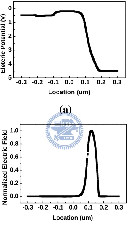
Fig. 3.2 The electric potential (a) and the (b) normalized electric temperature for split-gate SONOS
during programming.
Fig. 3.3 The drain current versus control-gate voltage with various drain voltages.
Fig. 3.4 The drain current versus drain voltage of conventional SONOS (red) and split-gate SONOS
(black).
Fig. 3.5 Simulated lateral electric field versus lateral position under (a) different control-gate
voltage and (b) measured programming window versus control-gate voltage.
application.
Fig. 3.8 The drain current versus gate voltage for split-gate SONOS with multi-level application. Fig. 3.9 The drain current versus gate voltage under forward read (open) and reverse read (void) for
dual-bit split-gate SONOS.
Fig. 3.10 The second-bit effect measurement for dual-bit split-gate SONOS.
Fig. 3.11 Illustration of gate disturbance (a) and the measured gate disturbance (b) for split-gate
SONOS.
Fig. 3.12 Illustration of drain disturbance (a) and the measured drain disturbance (b) for split-gate
SONOS.
Fig. 3.13 Illustrate Contour plot of potential distribution around gap between gates for a small
control-gate voltage (a) and a large control-gate voltage (b).
Fig. 3.14 The positive erasing transient with different control-gate voltage (a) and different
programming window (b).
Fig. 3.15 The retention loss measurement for one shot fresh cell (red) and 104 P/E (black) at 85C.
Chapter 4
Fig. 4.1 Diagram of VT profile in a programmed nitride storage memory cell (a) and the illustration
of Icp curves versus Vh before and after programming (b).
Fig. 4.2 Diagram of VT profile in a programmed nitride storage memory cell (a) and the illustration
of Icp curves versus Vb before and after programming (b).
Fig. 4.3 The charge pumping current versus Vh of program state (a) and erase state (b) after 1PE
cycle (left) and 10kPE cycles (right) for conventional SONOS.
Fig. 4.4 The charge pumping current versus Vh of a programmed cell after different numbers of P/E
cycles for conventional SONOS.
into the channel (b).
Fig. 4.6 Charge pimping characteristics (a), GIDL measurement (b) and deduced hole distribution
(c) of a over-erasing fresh cell, and subsequently after bake of 20k seconds at 150C.
Fig. 4.7 Schematic description of neutral trap formation in the bottom oxide.
Fig. 4.8 Schematic of charge loss of thermal activated electron trapped in the nitride trough traps
inside the bottom oxide (a). After loss of one of the trapped charges an additional percolation path can be generated (b).
Fig. 4.9 The schematic of misalignment between SSI and BBHH for split-gate SONOS.
Fig. 4.10 Dependence of threshold voltage on retention time in a fresh cell (a) and a 10k PE cell (b).
The gate biases are 0V, -3V and -5V.
Chapter 5
Fig. 5.1 Schematic for Vt(channel) and Vt(GIDL) (a) and the measured VtGIDL versus Vtchannel
with different word-gate length of split-gate SONOS (b).
Fig. 5.2 The programming and erasing transient of split-gate SONOS with different word-gate
length.
Fig. 5.3 Endurance of split-gate SONOS with different word-gate length.
Fig. 5.4 The drain current versus gate voltage at program state (a) and erase state (b) for split-gate
SONOS.
Fig. 5.5 Illustration of electrons, holes and interface state charge in cycled device being read at
program state (a) and erase state (b).
Fig. 5.6 The erasing transient for fresh cell (void) and 10k cycled cell (open) (a), and the illustration
for hole to inject after cycling (b).
the misalignment with different control-gate voltage (b).
Fig. 5.10 Endurance for split-gate SONOS with different control-gate voltages during erasing.
Fig. 5.11 Retention loss for split-gate SONOS with different control-gate voltages during erasing at
85oC.
Fig. 5.12 Experiment set up and timing diagram for STHH erasing, and its band diagram transient
during erasing.
Fig. 5.13 The oscilloscope trace of the amplitude of the voltage tested from drain (red) and substrate
(black) for the case of Vbase = 0V (a) Vbase = 1V (b) Vbase = 2V (c) with the same Vtop= 9V.
Fig. 5.14 The oscilloscope trace of the amplitude of the voltage tested from drain with pulse width of
50us (red) and 10us (black) (a), and the erasing window versus different pulse counts and widths (b).
Fig. 5.15 The threshold voltage shift with varying Vbase and Vtop.
Fig. 5.16 The charge pumping current versus Vh of fresh cell (black) and 10k cycled cell (b) for
conventional SONOS using STHH erasing scheme.
Fig. 5.17 The charge pumping current versus Vh of a programmed cell after different numbers of P/E
cycles for conventional SONOS using STHH erasing scheme.
Fig. 5.18 Forward read threshold voltage for various drain voltages for conventional SONOS using
STHH erasing scheme.
Fig. 5.19 Evolution of Dit with the number of P/E cycles endured by the device by using BBHH
erase (black) and STHH (red).
Fig. 5.20 Endurance for split-gate SONOS with different word-gate lengths by using STHH erasing
scheme.
Fig. 5.21 Retention loss for split-gate SONOS with different word-gate lengths by using STHH
Chapter 1
Introduction
1.1 The Motivation of This Work
Flash memories today are still mostly based on the storage of charges in the poly-silicon floating-gate (FG) of a MOS transistor. Since the storage medium is conductive, the device is subject to stress induced leakage current (SILC) because of traps accumulated in the bottom oxide during cycling. Thus, the scaling of bottom oxide below 8 nm is almost prohibited because of important charge loss after the cycling [1].
An alternative solution is to replace the floating-gate storage element by a non-conductive one, such as a nitride trapping layer [2]. This indeed makes the device much robust toward SILC, which explains the renewed interest for SONOS type flash memories. Nitride read only memory (NROM) cell is one of the most mature nitride based cells technologies [3]. This device is locally programmed by a channel hot electron injection (CHEI) and erased by a band-to-band tunneling hot-hole injection (BBTHHI), which allows the storage of two physically separated bits close to each junction and to use a thicker bottom oxide.
However, NROM device has following inherent disadvantages: (1) The channel length scaling is limited because the lateral distributions of the charges have to be
with CHEI and write disturbance due to the high drain voltage, and (3) The retention is strongly degraded after cycling. The repeated programming of each bit relies on a delicate overlap of the injected electrons and holes distributions, which is degraded as program/erase cycling proceeds. This can be followed by a drift and recombination of remaining charges after cycling. Besides, hot holes can be easily trapped in the bottom oxide during the erase operation, creating a path for vertical charge loss [4].
Here, the dual-bit split-gate SONOS is presented in this paper solves most NROM drawbacks while preserving the same performance, at the expense of a slightly more complicated processing. This structure allows separating both bit locations by a nitride layer, and prevents the charges from merging. The two bits are also addressed by separate gates, which remove the second bit effect. Furthermore, source-side injection can be used for programming. This mechanism is more efficient than CHEI, reducing the power consumption [4-6].
In this thesis, the characteristics and mechanisms of split gate SONOS will be discussed. Next, the retention loss mechanism will be investigated by using the split gate SONOS with different gate length. Then, an erase scheme called Substrate Transient Hot Hole Injection (STHHI) will be demonstrate to achieve low retention loss by suppressing the lateral retention loss [7-8]. Finally, we will draw a conclusion of this thesis.
1.2 Organization of the Thesis
Chapter 2, which includes the operating schemes, the program and erase schemes and the measuring method for charge pumping. In chapter 3, we will show the physical mechanism and the basic characteristics of the dual-bit split-gate SONOS. In Chapter 4, we will discuss the misalignment and retention loss model for conventional SONOS. In Chapter 5, we discuss the retention mechanism for split-gate SONOS by altering the word-gate length of the devices and demonstrate an erasing scheme for split-gate SONOS to achieve low retention loss. Finally, the conclusions will be presented in chapter 6.
Chapter 2
Device fabrication and Equipment Setup
2.1 Introduction
This chapter is divided into four sections. First of all, both split-gate SONOS and the conventional SONOS cells used in this study will be described. Second, the instruments setup and the experimental techniques to accurately control these instruments are illustrated. Third, we will discuss the programming and erasing schemes of these cells. Finally, charge pumping measurement technique setup used in this study will be demonstrated.
2.2 Device Fabrication
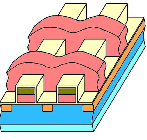
Figure 2.1 is the schematic diagram illustrating of forming the split-gate SONOS. As shown in Fig. 2.1(a), a substrate is provided, and a P well is formed in the substrate. Then, a plurality of control gate structure is formed on the P well. Each control-gate structure from bottom to top includes a gate insulating layer, a control gate oxide (65Å), and a cap nitride layer. As shown in Fig. 2.1(b), a silicon oxide layer (not shown), a nitride layer (not shown) is deposited on the substrate and control gate structure, and an etching back process is then performed to form a plurality of sacrificial spacers alongside each control gate structure. Meanwhile, a plurality of opening is formed between any two adjacent sacrificial spacers to expose the P well. Afterward, an implantation process is performed via each opening to form a plurality of N doped regions, serving as buried bit line, in the P well. As shown in Fig. 2.1(c),
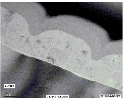
composite dielectric layer is formed on the P well, the control-gate structure, and the N doped regions. In this embodiment, the composite dielectric layer is an ONO tri-layer dielectric including a bottom oxide layer (60Å), a nitride layer (90Å), and a top oxide layer (90Å). As shown in Fig. 2.1(d), a conductive layer is entirely deposited on the composite dielectric layer, and a photolithography and etching process is performed to define a plurality of parallel word line, which are perpendicular to the control-gate structure, as shown in Fig. 2.1(e) [9]. The SEM image and the 2D-TCAD simulation structure of dual-bit split-gate SONOS are shown in Fig. 2.2 (a) and Fig. 2.2 (b). The gate width is 0.2um, and the channel length is 0.18um under control-gate and three different word-length(LWG) splits (0.13um,
0.12um, 0.10um) under word-gate.
The conventional SONOS device used in this study is first grown by thermal oxidation with thicknesses of 50 Å. Next, a layer of 60 Å LPCVD nitride film is grown. Finally, the LPCVD blocking oxide is grown with thickness of 50 Å. (W/L=0.7/0.26 um)
2.3 Equipment Setup
The experimental setup for the I-V and transient characteristics measurement of SONOS is illustrated in Fig. 2.3. Based on the PC controlled instrument environment via HP-IB (GP-IB, IEEE-488 Standard) interface, the complicated and long-term characterization procedures during analyzing the intrinsic and degradation behaviors in SONOS cells can be easily achieved. As shown in Fig. 2.2, the characterization
station provides an adequate capability for measuring the device I-V characteristics and executing the SONOS cell program/erase operation.
Source-monitor units (SMU) and provided the high current resolution to 10-15A range facilitates the gate current measurement, sub-threshold characteristics extraction, and the saturation drain current measurement. The HP E5250A equipped with a 10-input (6 SMU ports and 4 AUX ports) × 12-output switching matrix, switches the signals from the HP 4156C and the HP 8110A to device under test (DUT) in probe station, automatically. In addition, the HT-Basic are used as the program languages to achieve the personal computer (PC) control of these measurement instruments.
2.4 Programming and Erasing Setup
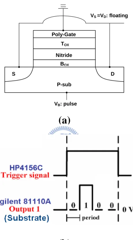
The general programming and erasing schemes for the conventional SONOS are Channel Hot Electron Injection (CHEI) and Band-to-Band Tunneling Hot Hole Injection (BBTHHI). For CHEI programming, source and substrate are grounded, while gate and drain are connected to the pulse generator as shown in Fig. 2.4 (a). The pulse timing diagram for both gate and drain are shown in Fig.2.4 (b). For BBTHHI erasing, substrate is grounded, and gate and drain are connected to the pulse generator just like CHEI, but keeps bulk floating this time as shown in Fig. 2.5 (a). The pulse timing diagram for both gate and drain are shown in Fig.2.5 (b).
Another erase scheme called Substrate Transient Hot Hole Injection (STHHI) is also used in this study. For STHHI, source and drain keep floating and gate is
The operation mechanism and relevant measurement of STHHI will be discussed after this chapter.
Dual-bit split-gate SONOS operates as conventional does, but adding a control-gate bias in the middle of the cell. The control-gate keeps a small constant bias for programming, while floating for erasing. And the other terminals are just the same as conventional operation.
2.5 Charge Pumping Measurement Technique Setup
The charge pumping measurement technique setup is shown in Fig. 2.6, which we called fixed based charge pumping, but with some method unlikely the traditional one. The pulse generator is connected to the gate, and with the substrate and drain connecting to the HP4156C, while source is kept floating. Fig. 2.7 (a) shows the pulse series type sending out from the pulse generator used by this setup. By using this setup, we can measure the charge pumping current from drain. If one wants to measure the charge pumping from drain (/source), we should connect the HP4156C with them and open the source (/drain) to get the information of the charge pumping current. The second scheme for charge pumping measurement technique setup is shown in Fig. 2.7 once again. However, the pulse series type is different this time. As shown in Fig. 2.7 (b), we used likely the traditional fixed top charge pumping pulse series to do our measurement.
(a)
(a)
(e)
Fig. 2.1 The schematic diagram illustrating of forming the dual-bit split-gate
(a)
(b)
Fig. 2.3 The experimental setup of the current-voltage and the transient
characteristics measurement. An automatic controlled characterization system is setup based on the PC controlled instrument environment.
01000 Probe Station Personal Computer HP 81110A Pulse Generator Parameter Analyzer HP 4156C Switch Matrix HP 5250 A
(a)
(b)
Fig. 2.4 The operation scheme (a) and time diagram (b) for CHEI programming.
S D VG: pulse VD: pulse BOX TOX Nitride P-sub Poly-Gate
(a)
(b)
Fig. 2.5 The operation scheme (a) and time diagram (b) for BBTHHI erasing.
S D VG: pulse VD: pulse BOX TOX Nitride VS: floating P-sub Poly-Gate
(a)
(b)
Fig. 2.6 The operation scheme (a) and time diagram (b) for STHHI erasing. S D BOX TOX Nitride VS =VD: floating P-sub Poly-Gate VB: pulse
(a)
(b)
Fig. 2.7 The operation scheme for charge pumping with fixed base pulse series
sketch (a) and fixed top sketch (b).
S D VG: pulse VD: Icp,d BOX TOX Nitride VS: floating P-sub Poly-Gate
(or Icp,s) (or floating)
S D VG: pulse VD: Icp,d BOX TOX Nitride VS: floating P-sub Poly-Gate
Chapter 3
Basic Characteristics of Dual-Bit Split-Gate SONOS
3.1 Introduction
In this chapter, first, we will introduce the basic physical mechanism of split-gate SONOS and find the optimized bias condition for both programming and erasing. Then, some reliability issues for non-cycled cell, such as gate disturbance, drain disturbance, second bit effect, and one shot retention will be discussed in this chapter.
3.2 Basic Mechanism and Optimized Bias Condition of Split-Gate
SONOS
3.2.1 Source Side Injection Programming
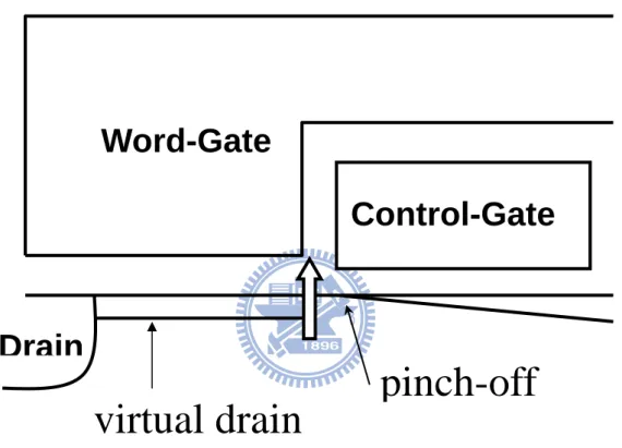
Channel hot electron injection has been widely used as a programming mechanism in flash memory. Based on Lucky-Electron model, the programming efficiency of flash memory is evaluated with the gate current or the substrate current as the figure of merit. Source side injection has a higher programming efficiency than drain-side programming by using-split gate structure to achieve high CHE generation and optimal electron collection at the same time. As shown in Fig. 3.1, under the programming condition, the word-gate is biased at a higher potential than the drain.
that the channel electrons are accelerated in this gap region and become hot enough to inject into the ONO layer underneath the word-gate as shown in Fig. 3.2 [5, 10-11].
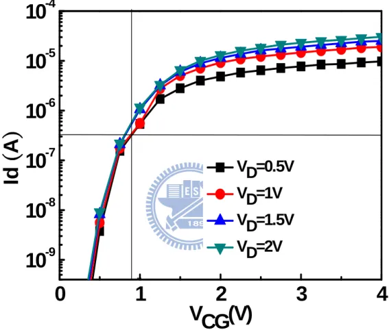
The drain current as a function of the control-gate voltage (VCG) for the
word-gate voltage (VWG) of 10V is shown in Fig. 3.3. The parameter was the drain
voltage (VD) varied from 0.5V to 2V. This bias condition makes the channel resistance
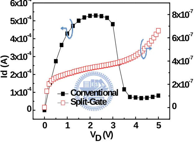
beneath the word-gate negligible small. Thus, the programming current was limited by the control-gate and is could be estimated to be 0.3uA in Fig. 3.3. Fig. 3.4
compares the drain current versus drain voltage curve between split-gate SONOS and conventional SONOS. It was found that the drain current for split-gate SONOS by using SSI is about 100~1000 times lower than conventional SONOS by using CHEI [4-5].
3.2.2 Optimized Control-Gate Voltage (VCG)
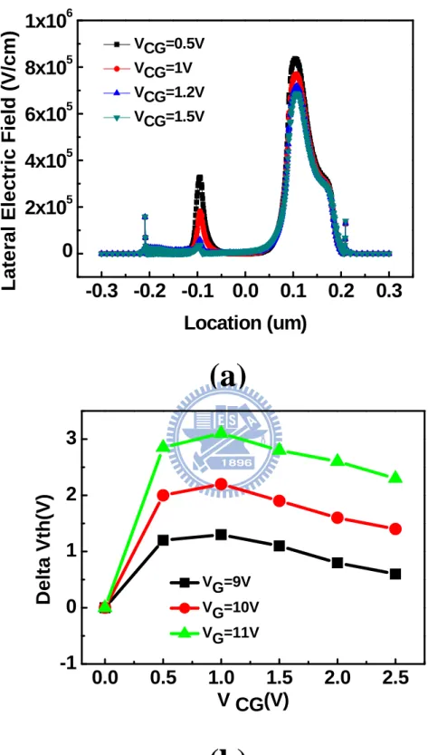
Figure 3.5 shows the simulated and measured result with different control-gate bias under programming. It shows the property bell-shape with respect to the VCG. In
split-gate SONOS memory device, the control-gate can limit the programming current, as mentioned above. This programming characteristic indicates that the control-gate can dominate not only the programming current but also the programming properties. When a large voltage than the threshold voltage against the channel beneath the control-gate is applied to the control-gate, the potential beneath the control gate is dropped down due to the effect of the drain voltage. This potential drop induces a fall in the lateral electric field, which is a derivative of the potential, in the gap between
channel. However, when a smaller voltage then threshold voltage of the control-gate is applied to the control-gate, the drain voltage does not induce a potential drop beneath the control-gate. This indicates that the drain voltage does not induce the drop of the lateral electric field in the gap. Instead the electric field formed at the gap is high enough to inject electron, however, the control-gate shuts off the programming current. Thus, electron can not be injected, even though a high electric field is formed at the gap. Therefore, to achieve high efficiency programming operation, both the programming current and the electric field must be obtained by applying the bias condition appropriately [5-6, 10].
3.2.3 Optimized Drain Voltage (VD)
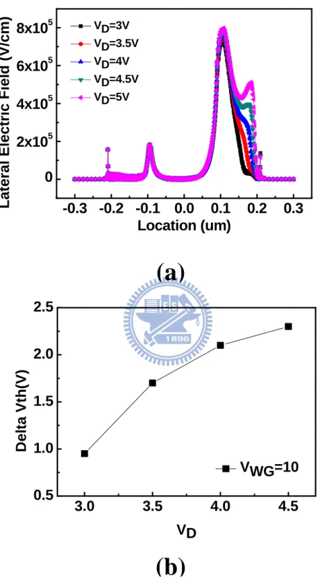
Figure 3.6 shows the simulated and measured result with different drain bias under programming. The shift in the threshold voltage was saturated against increases in the drain voltage. In the simulation result, drain voltage of over 3V does not affect the electric field at the gap except for increases the electric field at the junction. Therefore, it is no use by adding a too large voltage at junction but a proper voltage can achieve the same efficient as large drain voltage does [5-6].
3.2.4 Programming, Erasing Transient and Readout
Figure 3.7 shows the programming (VWG= 9V, 10V, 11V VD= 4V VCG= 0.9V
different read bias conditions. It was found that, if the read voltage is not large enough (o.1V), there is no threshold voltage difference between forward read and reverse read, since the program charge can not be completely depleted or the surface potential can not be pull down. Therefore, a large reverse read voltage (1.8V) is needed for readout for this type of memory cell to suppress the potential barrier, causing a local DIBL effect that screen out the potential barrier [4-5, 12-13]. The suggestion of programming, erasing and readout bias condition is shown in table 1.1.
3.3 Reliability for Non-Cycled Split-Gate SONOS
3.3.1 Second bit Effect
Figure 3.10 shows the second bit effect of the dual-bit split-gate SONOS. It was found that the left and right bit will not interfere with the other bit, since the two storage bit position is already separated by the control-gate. And the readout voltage of 1.8V is large enough to screen out the potential barrier [13].
3.3.2 Gate and Drain Disturbance
Fig. 3.11 and Fig. 3.12 show the gate and drain disturbance of the split-gate SONOS respectively. During programming and erasing, the selected row (column) applies to a word-gate (drain) voltage. Therefore, non-selected cell will suffer from gate (drain) disturbance as shown in Fig. 3.11 (a) and Fig. 3.12 (a). Fig. 3.11 (b) and
3.3.3 Another Erasing Method (Positive BBTHHI Erase)
There is another erase method like drain disturbance for split-gate SONOS. However, the erase speed for drain disturbance in Fig. 12 is too slow. Fig. 13 shows the contour plots of the potential distribution around the gap between the gates at the drain voltage of 6V. The voltage of the control-gate was small (0.9V) in Fig13 (a) and large (6V) in Fig13 (b). The potential for holes beneath the region where the electrons were trapped was lower than that around the region. It means that most of holes generated at the drain flow toward not only the substrate but also the electron trapped region. By comparing with Fig13 (a) and Fig13 (b), the potential induced by the voltage applied to the control-gate tend to spread beneath the gap by applying the higher voltage of the control-gate. This spread potential makes a path where hot holes generated at the drain region moving toward the substrate narrower than the path without the bias to the control-gate. This introduces more hot holes move toward the region where electrons are trapped than toward the substrate. Therefore, the larger positive voltage is applied to the control-gate, the more effectively the erasing operation using hot holes can be achieved without a negative bias [5].
Figure 14 shows the positive bias erasing transient with different positive bias applying to the control gate. For small positive control-gate bias (3V), most of the holes are flowing to the substrate. While large positive control-gate bias (6V), the holes are flowing into the nitride layer to achieve more efficient erase operation. However, large control-gate bias positive BBHH erase still need more time to
3.3.4 Retention Loss
Figure 15 shows the retention loss at program state for fresh and cycled cell. It was found that there is no loss for fresh cell but not for cycled cell. It is because after cycling, the bottom oxide is heavily damaged and a large amount of holes accumulate near junction causing both vertical and lateral retention loss, which will be discussed in the following chapters in detail.
Fig. 3.1 Schematic illustration of source-side injection for split-gate structure
SONOS flash memory.
pinch-off
Control-Gate
Word-Gate
virtual drain
(a)
(b)
Fig. 3.2 The electric potential (a) and the normalized electric temperature (b) for
split-gate SONOS during programming.
-0.3 -0.2 -0.1
0.0
0.1
0.2
0.3
5
4
3
2
1
0
E
letcric P
o
tential (V
)
Location (um)
-0.3 -0.2 -0.1 0.0
0.1
0.2
0.3
0.0
0.2
0.4
0.6
0.8
1.0
No
rm
aliz
ed Elect
ric Field
Location (um)
Fig. 3.3 The drain current versus control-gate voltage with various drain voltage.
0
1
2
3
4
10
-910
-810
-710
-610
-510
-4Id
(
A
)
VCG(V)
VD=0.5V
VD=1V
VD=1.5V
VD=2V
Fig. 3.4 The drain current versus drain voltage of conventional SONOS (red) and
split-gate SONOS (black).
0
1
2
3
4
5
0
1x10
-42x10
-43x10
-44x10
-45x10
-46x10
-40
2x10
-74x10
-76x10
-78x10
-7Conventional
Id (A
)
VD (V)
Split-Gate
(a)
(b)
Fig. 3.5 Simulated lateral electric field versus lateral position under (a) different
0.0
0.5
1.0
1.5
2.0
2.5
-1
0
1
2
3
VG=9V VG=10V VG=11VDel
ta Vt
h
(V
)
V CG(V)
-0.3 -0.2 -0.1 0.0
0.1
0.2
0.3
0
2x10
54x10
56x10
58x10
51x10
6 VCG=0.5V VCG=1V VCG=1.2V VCG=1.5VLate
ral Ele
c
tr
ic Field (V/cm
)
Location (um)
(a)
(b)
Fig. 3.6 Simulated lateral electric field versus lateral position under (a) different
drain voltage and (b) measured programming window versus drain voltage.
-0.3 -0.2 -0.1
0.0
0.1
0.2
0.3
0
2x10
54x10
56x10
58x10
5 VD=3V VD=3.5V VD=4V VD=4.5V VD=5VLatera
l Ele
c
tric Fie
ld (V/cm)
Location (um)
3.0
3.5
4.0
4.5
0.5
1.0
1.5
2.0
2.5
Del
ta Vth
(V)
VD
VWG=10
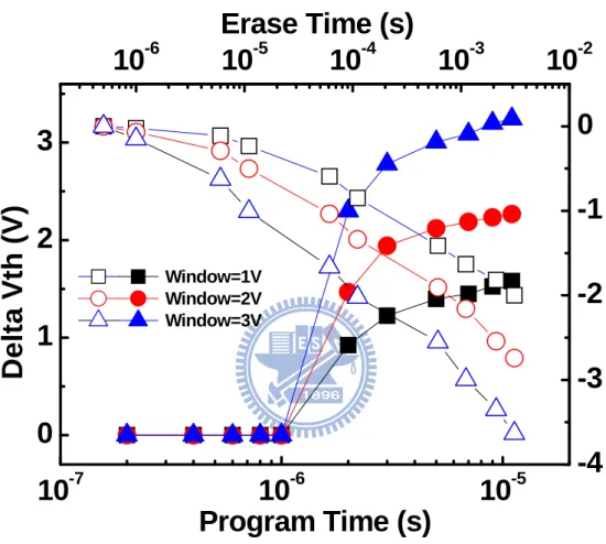
Fig. 3.7 The programming and erasing transient for split-gate SONOS with
multi-level cell application.
10
-710
-610
-50
1
2
3
10
-610
-510
-410
-310
-2-4
-3
-2
-1
0
Delta V
th (V)
Program Time (s)
Window=1V Window=2V Window=3VErase Time (s)
Fig. 3.8 The drain current versus gate voltage for split-gate SONOS with multi-level
application.
0
2
4
6
8
10
-1110
-1010
-910
-810
-710
-610
-510
-4Initial State
Window=1V
Window=2V
Window=3V
Id (A
)
VG (V)
Fig. 3.9 The drain current versus gate voltage under forward read (open) and reverse
read (void) for dual-bit split-gate SONOS.
0
2
4
6
8
10
10
-1210
-1110
-1010
-910
-810
-710
-610
-510
-4fresh VD=0.1V
fresh VD=1.8V
Pro VD=0.1V
Pro VD=1.8V
Pro Vs=0.1V
Pro Vs=1.8V
Id (A)
VG (V)
SSI
BBHH
STHH
Read
V
G9/10/11 -5
0 Sweep
V
CG0.9 floating
floating 2.1
V
D4 6
floating 0
V
S0
floating
floating
1.8
V
B0 0 10-2
0
Fig. 3.10 The second-bit effect measurement for dual-bit split-gate SONOS.
0.0
0.5
1.0
1.5
2.0
2.5
3.0
2.0
2.5
3.0
3.5
4.0
4.5
5.0
5.5
6.0
Vth of bit 2 (V)
Vth of bit 1 (V)
(a)
(b)
Fig. 3.11 Illustration of gate disturbance (a) and the measured gate disturbance (b)
for split-gate SONOS.
10
-710
-610
-510
-410
-310
-210
-110
010
110
23.0
3.5
4.0
4.5
5.0
Vth(V)
Time(s)
VG=14V VG=13V VG=12V VG=11VSelect
VG=11,12,13,14V VB=0V VSG,VD,VSfloating(a)
(b)
Fig. 3.12 Illustration of drain disturbance (a) and the measured drain disturbance (b)
Select
VG= floating VB=VS=0 VSG=0.9 VD=4,5,610
-610
-510
-410
-310
-210
-110
010
12
3
4
5
6
Vth
(V)
Time(s)
VBL=6V VBL=5V VBL=4V(a)
(b)
Fig. 3.13 Illustrate Contour plot of potential distribution around gap between gates
for a small control-gate voltage (a) and a large control-gate voltage (b).
1V
6V
6V
6V
(a)
(b)
Fig. 3.14 The positive erasing transient with different control-gate voltage (a) and
10
-610
-510
-410
-310
-2-2.0
-1.5
-1.0
-0.5
0.0
VCG=3V
VCG=6V
Delta Vth (V)
Erase Time (s)
10
-510
-410
-310
-2-3.0
-2.5
-2.0
-1.5
-1.0
-0.5
0.0
Window=1V
Window=2V
Window=3V
Del
ta V
th
(V)
Retention Time (s)
Fig. 3.15 The retention loss measurement for one shot fresh cell (red) and 104 P/E (black) at 85C.
10
010
110
210
310
4-2.0
-1.5
-1.0
-0.5
0.0
0.5
Fresh cell
cycled cell
Delta Vth (V)
Retention Time (s)
Chapter 4
Misalignment of Distributions and Retention Loss
Mechanisms for Conventional SONOS
4.1 Introduction
In this chapter, we will discuss the misalignment between the distribution of electrons and holes and the retention mechanisms for conventional SONSO flash memory. First, we discuss the mismatch distribution by using floating S/D charge pumping method. Next, we still use charge pumping method to analyze holes migration in the nitride storage layer. Finally, we explain both vertical and lateral retention loss mechanisms.
4.2 Principle of Charge Profile by Charge Pumping Method
4.2.1 Principle of Charge Pumping Method
The charge pumping method has been widely used for hot-carrier-related reliability characterization in MOSFETs. During a typical charge pumping measurement, a pulse string is applied to the gate terminal of a MOSFET while the substrate current (commonly called the “charge pumping current”) is monitored. Since this current is a result of the recombination of majority carriers (coming from
is biased to inversion), to first order the charge pumping current (Icp) is nonzero only
if the high level (Vh) and the base level (Vb) of the gate pulses cover both the
threshold voltage and the flat-band voltage [14-15].
Unlike the conventional charge pumping (CP) method, the other two basic ways of charge pumping test to attain the profile scheme are demonstrated. First one is the fixed base CP (fixed base level and varying the top level) method with one side of drain (or source) floating and the other one is the fixed top CP (fixed top level and varying the base level) method with also one side of drain (or source) floating, which are defined as FVb and FVh, respectively.
In FVb CP method, the setup is shown in Fig. 2.5 (a) in chapter 2, the gate is
applied with a pulse string, as shown in Fig. 2.5 (b), and the Icp can be measured from
drain or source side with source or drain floating respectively. When measuring the charge pumping current Icp,d from the drain side, the minority carrier only contributed
from the drain side and vice versa with Icp,s. Therefore, we can obtain more precious
information about the drain and source side from Icp,d and Icp,s. By combining these
two currents, we can profile the asymmetrical threshold voltage along the channel for both virgin and programmed cells [16-17].
4.2.2 Fixed Base Charge Pumping Method
Figure 4.1 (a) illustrates the threshold voltage profile of a programmed nitride storage memory cell, which contains a narrow threshold voltage peak near the drain
source junction area in Fig. 4.1 (a). After programming, localized trapped charges enhance the threshold voltage near drain side, which forms the asymmetrical threshold voltage profile in Fig. 4.1 (a). Therefore, the Icp,d and Icp,s curves shift
toward the right, which corresponds to the regions B and C in Fig. 4.1 (b). The difference between curves B and C indicates the location and profile of the injected charges. As Fig. 4.1 (b) shows, the injection is closer to the drain side. It needs to be pointed out that Icp keeps shifting rightward in region D, indicating a threshold
voltage peak here. Moreover, Icp,d and Icp,s overlap in this region, which means the
minority carrier coming from drain or source is passing through the peak region under the channel. For this reason, the equivalent interface traps are sensed and contribute the same Icp,d and Icp,s. Thus, in FVb CP method, data obtained in region D cannot be
used to extract the exact profile of threshold voltage in large current region. We can, however, extract the accurate location using this method.
4.2.3 Fixed Top Charge Pumping Method
On the other hand, the equipment setup is similar to FVb CP method instead of
the gate pulse string which is fixed on a constant level upon the threshold voltage. In contrast, the Icp curve shift caused by the threshold voltage peak, takes place in the
low current region and has higher precision in FVh CP method. Fig. 4.2 (a) illustrates
Icp test with FVh CP method in logarithmic scale. Correspondently, region B, C and D
in Fig. 4.2 (a) and Fig. 4.1 (b) also can be seen herein. Icp in region D can be used to
to identify the location.
4.3 Misalignment Between Electron and Hole Distribution
Fig. 4.3 shows the measured charge pumping curve for both program state Fig. 4.3 (a) and erase state 4.3 (b) after 1 and 10k P/E cycles. For program state, after the first program operation, the program charges are injected into the nitride layer near the junction, therefore, the charge pumping curve tested from drain raise up late because of a high local threshold voltage near the drain. However, after thousands of P/E cycles, the curve tested from source raise up late than tested from drain, which is totally contrary to the initial state. It is because after large numbers of PE cycles, the misalignment distribution of electron and hole makes a large amount of holes accumulation near the drain, inducing the local threshold voltage lowering near the junction. Fig. 4.4 shows the charge pumping measurement for the program state after different numbers of P/E cycles. The leftward shift of curves indicates the accumulation of holes near the junction.
While for erase state, after first erase operation, the charge pumping curves tested from drain and source are the same curve, since there is no program charge in the channel. But after hundreds or thousands of P/E cycles operation, the two curves are split off as increasing the number of P/E cycles. It is because the misalignment makes the electrons accumulation in the channel, which can not be recombined by the hot holes.
ionization position move toward in to the channel, making the mismatch more serious.
Fig. 4.5 shows the forward read threshold voltage measurement for various drain voltages. The saturation level of the curve is increasing with the number of cycles, which indicates the accumulation of electron far from the drain. It needs a larger drain voltage to completely deplete the program charge [18-22].
4.4 Hole Migration
In order to investigate the behavior of large amount of holes near the drain as discuss above. A fresh cell is initially over-erased. The charge pumping result is shown in Fig. 4.6 (a). The generated interface traps during erase are negligible since the Icp at Vh=5V is almost unchanged. Because a considerable amount of holes are
injected into the nitride layer after erase, a leftward shift of the low Vh portion (for
Vh<3.8V) of the Icp characteristic is observed. The cell is then baked at 125C. The up
sift of the Icp curve indicates the hole above the drain spread out into the channel. A leftward than rightward sift of Icp curve with baking time can be observed, however, the gate induced drain leakage current (GIDL) shift rightward as baking time increasing as shown in Fig 4.6 (b). Hence, the holes distribution can roughly be deduced as shown in Fig. 4.6 (c). The peak of the hole distribution should be in the drain as black curve. As the hole spread out, the distribution of hole become to the red than green curve, and result in the local threshold voltage at the end of drain increase first than decrease [23].
4.5 Retention Loss Mechanisms
4.4.1 Retention Loss Mechanisms for Conventional SONOS
Two main model types have been published to explain the retention mechanism. The first model explains the retention loss by lateral redistribution of charge as discuss above. During cycling, both holes and electrons accumulate in the nitride layer due to mismatch between the distributions resulting from the program and erase operation. The holes are de-trapped by thermal activation in the nitride layer and move toward the electron before recombining [21, 24-26].
The second model of retention is the vertical loss of charge through the bottom oxide. During cycling, the bottom oxide is progressively degraded by successive programming and erasing operation, which allows a trap assist tunneling through the bottom oxide [26-28]. Fig. 4.7 explains the generation of trap sites in the bottom oxide during P/E cycling and opens a vertical leakage path between the nitride layer and the substrate. Every trapped charge builds up a potential barrier for the inversion channel charges. After the loss of one of the trapped charge, an additional percolation path can be generated and therefore a higher drain current will flow as shown in Fig. 4.8 [29-30].
4.4.2 Retention Loss Mechanisms for Split-Gate SONOS
can adjust the word-gate length to improve the mismatch and suppress the lateral retention loss, which we will discuss in the next chapter. However, the vertical direction retention loss is inevitable. Fig. 4.10 shows the threshold voltage evolution with retention time in a fresh Fig. 4.10 (a) and in a cycled Fig. 4.10 (b) split-gate cell with different gate bias are applied. No charge loss is observed for the fresh cell, since the bottom oxide is clean for a fresh cell. While the retention loss for a cycled cell is dependant on applied gate bias caused by vertical direction retention loss.
(a)
(b)
Fig. 4.1 Diagram of VT profile in a programmed nitride storage memory cell (a) and
(a)
(b)
Fig. 4.2 Diagram of VT profile in a programmed nitride storage memory cell (a) and
(a)
(b)
Fig. 4.3 The charge pumping current versus Vh of program state (a) and erase state
(b) after 1PE cycle (left) and 10kPE cycles (right) for conventional SONOS.
2 4 6 8 0 50p 100p 150p fresh Icp (A) Vh (V) 2 4 6 8 0 100p 200p 300p 400p 500p cycled
tested from drain tested from source tested from drain
tested from source
Vh (V) 2 4 6 8 0 50p 100p 150p fresh Icp (A) Vh (V) 2 4 6 8 0 100p 200p 300p 400p 500p 600p cycled
tested from drain tested from source tested from drain
tested from source
Fig. 4.4 The charge pumping current versus Vh of a programmed cell after different
numbers of P/E cycles for conventional SONOS.
3
4
5
6
7
0
100p
200p
300p
400p
500p P:CHEI E:BBHH
I cp
(A)
Vh (V)
1P
10PE
100PE
1000PE
10000PE
(a)
(b)
Fig. 4.5 Forward read threshold voltage for various drain voltages (a). The
accumulated electrons and holes may alter the current flowing path and
0.4
0.8
1.2
1.6
2.0
3.5
4.0
4.5
5.0
5.5
P:CHEI E:BBHH
1P 10PE 100PE 1000PE 10000PEVth (V)
VD (V)
With increasing PE cycle numbers h e Before cycling After cycling(a)
(b)
2
3
4
5
1p
10p
100p
I cp
(A)
Vh (V)
fresh over erase 1000s bake 10000s bake 20000s bake-6
-4
-2
1E-12
1E-11
1E-10
Id (A
)
VG (V)
over erase 1000s bake 10000s bake 20000s bake(c)
Fig. 4.6 Charge pimping characteristics (a), GIDL measurement (b) and deduced
hole distribution (c) of a over-erasing fresh cell, and subsequently after bake of 20k seconds at 150C.
(a)
(b)
Fig. 4.8 Schematic of charge loss of thermal activated electron trapped in the nitride
Fig. 4.9 The schematic of misalignment between SSI and BBHH for split-gate SONOS.
Control gate
L
WGWord gate
Drain
electron
hole
(a)
(b)
Fig. 4.10 Dependence of threshold voltage on retention time in a fresh cell (a) and a
10k PE cell (b). The gate bias is 0V, -3V and -5V.
1
10
100
1000
10000
-2.0
-1.5
-1.0
-0.5
0.0
0.5
V th(V)
Retention Time(s)
VG=0V
VG=-3V
VG=-5V
10
010
110
210
310
4-2.0
-1.5
-1.0
-0.5
0.0
0.5
V th(V)
Retention Time(s)
VG=0V
VG=-3V
VG=-5V
Chapter 5
Retention Loss Mechanism and Methods to Suppress
Lateral Retention Loss for Split-Gate SONOS
5.1 Introduction
Different from conventional SONOS, the split-gate SONOS can adjust the word-gate length (sacrifice spacer length) or the control-gate bias under the erase operation to reduce the misalignment and suppress the lateral retention loss. By comparing the split-gate SONOS with different word-gate length, we can separate the vertical and lateral retention loss, which can not be achieved in conventional SONOS.
In this chapter, we will first compare the retention loss with different word-gate lengths. Next, we compare the retention loss by using positive and negative erase method, which is introduced in chapter three. Then, we contrast the retention loss by applying different control-gate bias under erase operation. Finally, we demonstrate an erasing scheme to suppress the lateral retention loss for all kind of word-gate length devices and discuss the retention loss mechanism for the split-gate SONOS device.
5.2 Retention Loss with Different Word-Gate Length
operation does. It is because the shorter word-gate length device makes the injected electron more close to the junction. Thus, a shorter word-gate length is favorable for the compensation of electron by hole. Fig. 5.2 shows the VGIDL versus Vchannel for the
split-gate SONOS with different word-gate lengths. Since the GIDL current is sensitive to the charge above the junction, we can use this method to compare the injected electron distributions. In Fig. 5.2 (b), the shorter word-gate length device has larger slope, since the program charge is injected more close to the junction than long word-gate length device [4, 31-33]. It is worth noting that under GIDL measurement, the drain pulse is applied of 3V to suppress another impact ionization in the junction, which has been discussed in chapter three.
Fig. 5.3 shows the endurance of the three devices. An important increase of erase state threshold voltage is observed, and the situation becomes better for shorter word-gate length device because of the different injection point of electrons and holes. While for the program state, the threshold voltage has only a little decreasing at first than increasing at last. The incensing of program state threshold voltage is also induced by misalignment, but the decreasing of threshold voltage is cause by interface degradation and non-uniform nitride charge distribution [34]. Fig. 5.4 shows the drain curve versus gate voltage for program state and erase state after different P/E cycles. It was found that the sub-threshold swing is strongly degraded after large number of successive programming and erasing operation for program state, resulting from the generation of interface state near the junction and resulting in decreasing of the threshold voltage. However, for erase state, the sub-threshold swing has only a little difference. It is because the “local inversion” region induced by excess holes in the
cycling for long word-gate device. It is due to hole accumulated in the nitride, or in the bottom oxide at the drain side, that cause a repulsive effect to the injection of holes in the next cycling as shown in Fig. 5.6 (b).
Since we utilize the same programming and erasing condition for all three devices during cycling, we can assume the bottom oxide are equally damaged. Then, the program state retention loss between two devices is caused by lateral retention loss as shown in Fig. 5.7. It can be said that, vertical retention loss should dominate the total retention loss, however, under a large misalignment situation, the lateral retention loss will give an other non-negligible loss portion. For erase state, the retention loss first increase than decrease a little. The increasing of threshold voltage is cause by drift of holes jump out from bottom oxide into substrate, while the decreasing of the threshold is cause by lateral redistribution of holes in the nitride layer. The larger misalignment between electrons and holes distributions, the more serious of holes drift and lateral move can be observed.
5.3 Retention loss with different Control-Gate Bias
5.3.1 Positive Erase Versus Negative Erase
Fig. 5.8 shows the endurance between the negative and positive erasing scheme. Although the large positive control-gate bias can narrower the potential contour to make the hot hole injecting into the nitride layer, it will repulse the positive charge
5.3.2 Negative Erase with Adding a Control-Gate Bias
Therefore, we can change the holes distribution by using negative erase but adding a small control-gate bias instead of floating it. Fig. 5.9 shows the erase transient with applying different control-gate bias. A small negative control-gate bias can attract the holes close to the control-gate to make a faster erasing operation, on the contrary, a small positive control-gate bias may repulse the hot holes away from the control-gate to make a slower erasing operation [32]. Fig. 5.10 and Fig 5.11 show the endurance and retention. The misalignment of electrons and holes distribution can be improved by adding a small negative bias and degrade by adding a small positive bias. The lateral retention loss can be split off again, which verifies the lateral retention is caused by misalignment distribution of electrons and holes.
All in all, the spilt-gate SONOS is very flexible for adjusting the electrons and holes distributions, no meter by altering the word-gate length or by adding different control-gate bias.
5.4 An Erasing Scheme to Suppress Lateral Retention Loss
5.4.1 The mechanism of STHH Erase
Here, we propose an erase scheme to suppress the lateral retention loss. The set up is shown in Fig 2.6. The gate is grounded, and the source and drain are kept floating while apply a pulse to the substrate. The mechanism of this erasing scheme is
in voltage between drain and substrate. As time goes from T2 to T3, the substrate bias immediately back to Vbase, while the floating drain can not catch up but slowly back to
the initial position. Therefore, a large band banding occurs at the time from T2 to T3 and generates hot holes to achieve erasing operation. Although the applied pulse width can be micro-second or less, the real erasing time is the time for floating drain move from Vtop-Vbi to Vbase-Vbi. Therefore, we call this erase scheme Substrate
Transient Hot Hole erase [7-8, 35].
Fig. 5.13 shows the time versus voltage tested from substrate and drain during erasing at the same Vtop=9V but different Vbase. The lager Vbase –Vtop induces large
voltage drop to generate more hot holes. In Fig. 5.13, we can observe that the breakdown voltage of the p-n junction is about 7V, that is, the largest voltage drop is 7V. Fig 5.13 (a) is the case that allows 7V of drop, and the erase window is about 2.2V. However, the erase window in Fig 5.13 (b) is 2.8V with the same voltage drop of 7V. It is because the Vbase induces an electric field, making the hole more easily to inject
into the nitride layer. Although the larger Vbase induces the stronger electric field and
makes hole easily to jump into the nitride layer, the large Vbase could reduces the
voltage drop and reduces the erase window as shown in Fig 5.13 (c).
Fig. 5.14 shows the erasing window versus pulse width and pulse counts. Since the real erasing time is the RC time constant, the erase window has no relation with the pulse width. Fig. 5.15 shows erase window versus various of Vbase and Vtop. At
Vbase =2V, the enhancement of electric field become more stronger to make hole
injecting into nitride. However, the voltage drop is decreasing to decrease the erase window for Vtop=8V and 9V cases. The same result happens to Vbase =3V or higher.
All in all, the three important components determine the erase efficient: the voltage drop, the electric filed builds by Vbase and the RC time constant.
5.4.2 STHH Erase for Conventional SONOS
Fig. 5.16 shows the charge pumping measurement for conventional SONOS using CHEI programming and STHH erasing before and after cycling as discussed in chapter four. It was found that the curve does not change their position before and after cycling, which indicates less holes accumulation as shown in Fig 5.17 compared to Fig 4.4. Fig 5.18 shows the forward read threshold voltage of a programming cell after P/E cycle. The curves only have a little shift indicates less electrons accumulation in the channel. A great match between electrons and holes distributions can be achieve by utilizing the STHH erasing scheme to completely erase the program charges in the nitride layer. The interface state can also be calculated by using Fig. 4.4
and Fig 5.17. A small number of STHH will be generate is observed.
5.4.3 STHH Erase for Split-Gate SONOS
Fig. 5.20 shows the endurance of the split-gate SONOS with different word-gate length by using STHH erasing scheme. The erase state threshold voltage is almost independent of word-gate length because the STHH erasing scheme has a widely
state, both of them are independent of word-gate length because of a good match between electrons and holes. For program state, no split off between two curves indicates the suppression of the lateral retention loss. And because of low misalignment between electrons and holes, the remaining hole in the bottom oxide is low, too. Therefore, a small hole drift and lateral redistribution can be observed in the retention loss of erase state.