-i-
國立交通大學
材料科學與工程學系
博 士 論 文
以凱文錫球結構及有限元素分析法研究覆晶銲錫凸塊與微
凸塊的電遷移破壞機制
Study of Failure Mechanisms in Flip-Chip Solder Joints and
Microbumps under Electromigration Using Kelvin Bump
Structures and Finite-Element Analysis
研究生: 張元蔚
指導教授: 陳智
-ii-
以凱文錫球結構及有限元素分析法研究覆晶銲錫凸塊與微凸塊的電
遷移破壞機制
Study of Failure Mechanisms in Flip-Chip Solder Joints and Microbumps
under Electromigration Using Kelvin Bump Structures and
Finite-Element Analysis
研究生: 張元蔚
Student: Yuan-wei Chang
指導教授: 陳智
Advisor: Chih Chen
國立交通大學
材料科學與工程學系
博士論文
A Thesis
Submitted to Department of Materials Science and Engineering College of Engineering
National Chiao Tung University in partial fulfillment of the requirements
for the degree of Ph.D. in Materials Science and Engineering
August 2013
Hsinchu, Taiwan, Republic of China
-i-
摘要
於此研究中,共三種預先設計好、包含凱文錫球結構之銲錫凸塊被用於非破 壞性觀測電遷移測試時的電阻變化。 第一種是覆晶銲錫凸塊,其凸塊電阻小於 1 毫歐姆、成長時呈現凹口向上之 趨勢,直到凸塊電阻上升超過 10 毫歐姆時,會開始急遽上升而後斷路;內部對 應之微結構是孔洞的成核與成長,孔洞首先生成於電流集中區然後沿著介金屬化 合物與銲錫間介面成長,在測試的末期,電遷移導致的相粗化減緩了電遷移產生 的破壞,且可以發現孔洞在電遷移測試末期會分成兩段;且根據實驗結果,我們 計算得到一個可表達剩餘接觸面積與凸塊電阻的關係式。 第二種試片則是六微米高的微凸塊,其微凸塊電阻呈現凹口向下之行為,從 15 毫歐姆開始急遽增加,然後在測試 400 小時後達到一個定值,早期急劇增加 的幅度約 5 毫歐姆,這與有限元素分析法所得之結果相符;在電遷移測試中,陰 極金屬墊層會與銲錫反應並將整個微凸塊轉變為 Ni3Sn4,Ni3Sn4具有較銲錫佳之 抗電遷移特性,所以導致凸塊電阻維持一個定值;在不同角度的凸塊電阻指出了 電流集中效應雖然沒有發生在銲錫中,依舊發生在金屬墊層裡,對於微凸塊來說, 完整的電壓降應該是由 0 度所量到的值,而這個值比 180 度所得到的值高了 7 倍, 也就是說,其實微凸塊所造成的容/阻延遲相當的大;而為了要簡化描述微凸塊 電阻、電流集中比與凸塊尺寸的關係,一個數值分析模型在此被提出,根據此模 型,微凸塊電阻與電流集中的關係可以被表達為簡單的關係式。 最後一種試片則是十微米高的微凸塊,其電阻開始時呈現凹口向下,然後轉-ii- 變為凹口向上,原因在於,其銲錫的量太多,而無法被中介板端的金屬墊層消耗 完;開始時,凹口向下的反應行為與矮的微凸塊相當接近,不過因為銲錫的量太 多,所以在電子流向上(由中介板端流向晶片端)之微凸塊中,2 微米厚之鎳層 會受電遷移影響而融入銲錫中,當這些鎳用完以後,孔洞就會產生在這些金屬墊 層本來的位置上,且造成電阻曲線又轉變成凹口向上。 根據這些結果,由凱文錫球結構所獲得凸塊電阻的曲線行為經由有限元素模 型的幫助,可以在測試中用來檢視其微結構的變化,有限元素模型可以很清楚的 表現出不同電遷移階段電流密度的演進,因此可以幫助預測電遷移破壞的機制; 此外,凱文錫球結構與過去最常用於分析墊遷移之雛菊花環結構完全的相容,兩 個值可以在同時量測取得,此一點是凱文錫球結構之一大優勢。
-iii-
Abstract
In this study, three types of solder bump samples with Kelvin bump structures were employed to monitor non-destructively the evolution of resistance during electromigration (EM) testing.
The first type of sample was flip-chip bumps. The bump resistance was found to be less than 1 mΩ and increase as a concave-up curve. After the bump resistance increased to more than 10 times its initial value, it started to grow rapidly and then failure. The corresponding microstructure showed void nucleation and propagation. The void first formed near the current crowding spot and then grew along the interface between the intermetallic compound (IMC) and the solder. At the end stage of EM testing, phase coarsening caused by EM retarded the failure, and the void split into two parts. The relation between the remaining contact area and the bump resistance was calculated.
The second type of sample was 6-μm microbumps. The microbump resistance curve was concave-down. It started around 15 mΩ, increased rapidly in the beginning, and then reached a constant value after 400 hr of testing. The increase in the early stage of testing was around 5 mΩ, which was reasonable when compared with the results of finite-element models (FEMs). During EM testing, the cathode-side under-bump-metallization (UBM) reacted with the solder and transformed the entire microbump into Ni3Sn4. Ni3Sn4 has better EM resistance than the solder and caused
the bump resistance to remain at a constant value. The bump resistances at different angles indicated that current crowding still took place, but in the Cu UBM and not in the solder. The complete voltage drop across the microbump was the value obtained at
-iv-
0°. However, the bump resistance obtained at 0° was 7 times larger than that measured at 180°. That is, the RC delay caused by microbump is actually very large. For simplicity of description on the relation between microbump resistances, crowding ratio, and structural dimensions, a numerical model was built. The expressions of microbump resistance and the crowding ratio were also obtained.
The last type of sample was the 10-μm microbumps. The resistance behaved first concave-down and then concave-up because the solder was too much for the interposer-side UBM to consume. The concave-down curve was first observed for the same reason as that of the low-bump-height case. However, the height of the solder was around 10 μm, which was too high for the interposer-sider UBM to react with. When the electrons flow upward (from interposer to chip), the interposer-side UBM, 2-μm Ni, was the cathode side. Driven by EM, the-2μm Ni quickly dissolved into the solder. After the 2-μm Ni ran out, the void was formed, causing the bump resistance curve to become concave-up again.
The solder height affected the failure mechanism. When the solder height was 25 μm, void propagation was the main failure mechanism. When the solder height
decreased to 10 μm, the mechanism became the combination of void propagation and IMC growth. When it was 6 μm, the failure mechanism changed to IMC growth only. The FEM described clearly the evolution of current density distribution at various stages of EM and therefore helped predict accurately the failure mechanism. Moreover, the Kelvin bump structure is compatible with the generally used daisy chain structure. Both bump resistance and daisy chain resistance could be obtained at the same time.
-v-
致謝
能夠博士班就讀期間順利完成本研究,敝人的指導教授陳智老師自是功不可 沒,當我面臨研究瓶頸的時候不斷提供寶貴而適切的建議與幫助,而在成果豐碩 的時候也不吝於給予熱烈的鼓勵。此外,正所謂身教重於言教,陳智老師對於研 究積極的熱誠與付出更是令我尊敬的榜樣,也因為追隨著陳智老師這樣的目標, 本研究才得以順利完成。且於就學過程中,敝人經由陳智老師推薦而參與龍門計 畫,因而難能可貴的得到了一年在異鄉求學的經驗,其中的感謝之情難以言述。 除了陳智老師以外,細數求學的過程中,還有太多需要感謝的人。潁超學長、 重光學長、世緯學長、章斌學長、程昶學長等人,於我碩士班時期就給予我很多 指導,讓我很快地就融入實驗室,若不是你們紮實教會我諸多基本的實驗技巧, 本研究不可能進行的如此順利;與我有諸多合作、亦師亦友的聖翔學長在就讀博 士班的這幾年間也給了我很多實質的幫助;筱芸學姊就出國交流的準備工作給了 我很多建議,特別是在 UCLA 的期間給了我很多幫助,讓我很快地就融入異鄉的 生活;道奇學長、翔耀學長、詠湟學長、健民學長、佳凌學姊、宗寬學長、漢文、 右峻雖於研究上與我並無重大關聯,但於各自的研究領域皆有特殊的造詣,是我 十分尊敬的研究人員;以撒、韋嵐的研究領域雖與我沒有直接相關,但時常於我 有開放性的討論,讓我有機會可以對他們的研究有更多的認識,且對於一些心靈 與思想方面的討論,你們也給予我很多寶貴的意見;奕丞雖然因為逕讀博班的緣 故還是研究的新手,但其研究的熱誠、專注、細心是隱藏不了的,看著你也讓我 對於研究偶爾迷惘的心情又重新燃起熱情;若薇、秉儒、黎云等幾位,是我直接 指導過的學弟妹,非常感謝你們於實驗中細心聆聽我的交代並忍耐我在各方面的 堅持,其中若薇已為人妻,祝福妳的婚姻生活百年好合,而黎云目前尚未畢業, 也祝福妳在未來一年的碩士班生活中,一切研究順利;致嘉的思路靈活、做事紮 實,令我印象深刻,也默默改變了我對某些事物的看法;曉葳、朝俊、竣傑、玉 龍過去與我私底下有不少聊天的機會,謝謝你們替我舒緩了不少情緒。還有天麟、 育安、瑋安、建志、岱霖、韋奇、明墉、偉豪、俊毅、皆安、岱陽、順財、宛霖、 書漢,雖然因為我餐與龍門計畫加上有些是新進的成員,所以相處的時間不長, 但也讓我的研究生活多了許多樂趣,如果少了任何一個實驗室成員的話,我的研 究恐怕不會有現在的成果。 在此還要感謝我的口試委員台大材料的高振宏老師、清大材料的廖建能老師、 以及本所的張立老師在口試的過程中給予了很多珍貴的意見。 我的家人在我就讀博士班的過程中,儘管不懂我研究的目標,可是還是給我 心裡上與經濟上無條件、無上限的支持,讓我在研究的時候沒有後顧之憂。最後, 則是我摯愛的女友,感謝妳對於我忙碌、無法時時陪伴妳的理解,那溫柔、貼心 的包容總是令我備感溫暖。你們是我研究的背後看不見的大功臣,謝謝你們。-vi-
Contents
摘要 ... i
Abstract ... iii
致謝 ... v
Contents ... vi
Figure Captions ... ix
List of Tables ... xiv
Chapter 1.
Introduction ... 1
1.1.
Flip-Chip Technology ... 1
1.2.
Microbump Technology ... 4
1.3.
Electromigration ... 7
1.4.
Current Crowding Effect ... 11
1.5.
Failure Mechanisms of Solder Joints under Electromigration ... 15
1.6.
Interfacial Reaction ... 21
1.7.
Kelvin Sensing ... 22
1.8.
Finite-Element Method ... 25
1.9.
Motivation ... 26
Chapter 2.
Experimental ... 29
2.1.
Flip-Chip Solder Bumps ... 29
-vii-
2.1.2. Kelvin Bump Structures and Experimental Procedures ... 32
2.2.
Six-Micro-Meter Microbumps ... 36
2.2.1. Sample Structure ... 36
2.2.2. Kelvin Bump Structures and Experimental Procedures ... 39
2.3.
Ten-Micro-Meter Microbumps ... 42
2.3.1. Sample Structure ... 42
2.3.2. Kelvin Bump Structures and Electromigration Stressing Conditions ... 44
2.4.
Procedures of Finite-Element Modeling ... 44
2.4.1. Element Type and Materials Properties ... 45
2.4.2. Model Construction and Meshization ... 48
2.4.3. Boundary Conditions and Solution ... 49
2.4.4. Post-processing ... 51
2.5.
Models ... 51
2.5.1. Model of Flip-Chip bumps ... 51
2.5.2. Model of Microbumps ... 54
2.5.3. Model of Scallop Intermetallic Compounds ... 57
2.6.
Numerical Modeling of Current Crowding Effect ... 59
Chapter 3.
Results ... 63
3.1.
Electromigration Test Results of Flip-Chip Bumps ... 63
3.1.1. Bump Resistance of Flip-Chip Bumps ... 63
3.1.2. Microstructure Evolution in Flip-Chip Bumps ... 66
3.1.3. Void Growth Rate in Flip-Chip Bumps ... 71
3.2.
Electromigration Test Results of Six-Micro-Meter Microbumps ... 73
3.2.1. Bump Resistance of Six-Micro-Meter Microbumps ... 73
3.2.2. Microstructure Evolution in Six-Micro-Meter Microbumps ... 77
3.2.3. Bump Resistance at Different angles in Six-Micro-Meter Microbumps ... 83
3.3.
Electromigration Test Results of Ten-Micro-Meter Microbumps .. 85
3.3.1. Resistance of Ten-Micro-Meter Microbumps ... 85
3.3.2. Microstructure Evolution in TenMicro-Meter Microbumps ... 88
-viii-
3.4.1. Finite-Element Analysis of Scallop Intermetallic Compounds ...92
3.4.2. Finite-Element Analysis of Flip-Chip Bumps ...95
3.4.3. Finite-Element Analysis of Six-Micro-Meter Microbumps ...98
3.4.4. Finite-Element Analysis of Ten-Micro-Meter Microbumps ...102
Chapter 4.
Discussion ... 104
4.1.
Bump Resistance of Flip-Chip Bumps ... 104
4.2.
Secondary Void Formation near End Stage of Electromigration
Testing ... 109
4.3.
Bump Resistance of Six-Micro-Meter Microbumps ...113
4.4.
Relation between Bump Resistance Behavior and Microstructure
Evolution ...116
4.5.
Effect of Solder Height on Microstructure Evolution ...117
4.6.
Effect of Magnitude of Applied Current on Microstructure
Evolution ...119
4.7.
Integration between Kelvin Bump structures and Daisy Chain
Structure ...119
Chapter 5.
Conclusions ... 121
Chapter 6.
References (MLA format) ... 124
-ix-
Figure Captions
Figure 1-1 (a) Tilt-view SEM image of solder bumps array on silicon die [2]; (b) a
flip-chip solder joint connecting the chip side and the substrate side [2]; and (c) the chip placed upside down onto the substrate and the joint formed simultaneously between chip and substrate by reflow [1]. ... 3 Figure 1-2 (a) Difference between 2D and 3D structure in fabrication of integration
circuits [19]; and (b) difference between SIP/SoC and 3D-IC technology [22]. ... 6 Figure 1-3 (a) Blech’s structure, showing an aluminum strip deposited on a TiN layer
[2]; (b) morphology of a Cu strip tested for 99 hr at 350ºC with 5 × 10⁵ A/cm2 current density [2]; and (c) two-dimensional conductor with grain boundaries and intersections [2]. ... 10 Figure 1-4 (a) Line-to-bump geometry of a flip-chip solder bump joining an
interconnect line on the chip side (top) and a conduction trace on the board side (bottom) [13]; and (b) two-dimensional simulation of current distribution in a solder joint [13]... 13 Figure 1-5 (a) Oblique current density distribution in a solder joint with Ti/CrCu/Cu
thin-film UBM [31]; (b) cross-sectional current density distribution [31]; 3D current density distribution at the cross-section of (c) Y1, (d) Y2, (e) Y3, (f) Y4, (g) Y5, and (h) Y6 [31]. ... 14 Figure 1-6 SEM images of void formation and propagation in a flip-chip E-SnPb
-x-
and (c) 43 hr [16]; and (d) SEM image of void formation in a flip-chip 95.5Sn4.0Ag0.5Cu solder bump stressed at 146ºC by 3.67 × 104 A/cm2 [29, 33]. ...18 Figure 1-7 Solder joints current stressed at 140ºC by 2.55 × 104 A/cm2 for (a) 0 hr, (b)
3 hr, (c) 12 hr, (d) 18 hr, and (e) 20 hr [17]. ...19 Figure 1-8 Top region of a solder bump after current stressing of 1.6 × 10⁴ A/cm2 at
150ºC for (a) 30 min, (b) 60 min, (c) 100 min, and (d) 120 min [53]; (e) melted solder joint due to large Joule heating before an open circuit [53]; and (f) relationship between maximum temperature of bumps and resistance change of Al line [54]. ...20 Figure 1-9 (a) Two-wire sensing; (b) Kelvin sensing (4-wire sensing); (c) schematic
of Kelvin sensing structure applied in semiconductor fabrication industry [66]; and (d) Kelvin sensing structure fabricated [67]. ...24 Figure 2-1 (a) Schematic illustration in plan-view of an entire flip-chip sample; (b)
schematic illustration of the flip-chip solder bump; and (c) cross-sectional SEM image of a flip-chip solder bump. ...31 Figure 2-2 (a) Plan view and (b) front view of Kelvin bump structures in the
flip-chip sample. ...34 Figure 2-4 Kelvin bump structures in a 6-μm microbump. ...41 Figure 2-5 (a) Schematic plot and (b) cross-sectional SEM image of a 10-μm
microbump; (c) 10-μm microbump structure tested. ...43 Figure 2-6 SOLID69 Geometry. ...47 Figure 2-7 Procedures for building and solving a model. ...50 Figure 2-8 (a) Solid model cross-section of a flip-chip bump; (b) enlarged image of
-xi-
the black-line region in (a); (c) oblique view of the solid model; and (d) element model of a flip-chip bump. ... 52 Figure 2-9 Different stages of void nucleation and propagation during EM test. ... 53 Figure 2-11 (a) Cross-sectional view of solid model, (b) oblique view of solid model,
and (c) oblique view of element model of a 10-μm microbump... 56 Figure 2-13 (a) Schematic plot of numerical model for calculating the resistance of a
microbump; and (b) the corresponding resistance network diagram. ... 62 Figure 3-1 (a) Bump resistance curve of a flip-chip bump during EM test; (b)
enlarged bump resistance curve of the dashed square in (a); and (c) resistance of entire circuit in the flip-chip sample. ... 65 Figure 3-2 (a) Stage 0 (initial stage), (b) stage 1, (c) stage 2, (d) stage 3, (e) stage 4,
and (f) stage 5 of the failure caused by EM test... 68 Figure 3-3 Binary Pb-Sn phase diagram. ... 69 Figure 3-4 Plan-view X-ray image of (a) stage 2, (b) stage 3, (c) stage 4, and (d)
stage 5. ... 70 Figure 3-5 (a) Void depletion area at different stages during EM testing; and (b) void
depletion velocity along the interface at different stages during EM testing. ... 72 Figure 3-6 (a) Bump resistances and (b) increase in bump resistances of 6-μm
microbumps after current stressing by 0.12 A (4.6 × 10⁴ A/cm2) on 150ºC hot plate for different durations. ... 75 Figure 3-7 (a) Bump resistances and (b) increase in bump resistances of 6-μm
microbumps after current stressing by 0.24 A (9.2 × 10⁴ A/cm2) on 150ºC hot plate for different durations. ... 76
-xii-
Figure 3-8 6-μm microbumps in samples EM tested for (a) 49.8 hr, (b) 321.6 hr, and (c) 1961.8 hr by 0.12 A (4.6 × 10⁴ A/cm2) on 150°C hot plate. ...81 Figure 3-9 6-μm microbumps in samples EM tested for (a) 141.3 hr and (b) 192.3 hr
by 0.24 A (9.2 × 10⁴ A/cm2) on 150°C hot plate. ...82 Figure 3-10 Bump resistance of 6-μm microbumps at different angles and trace
resistance of t5-6. ...84
Figure 3-11 (a) Bump resistance and (b) increase in bump resistance of 10-μm microbumps during EM testing. ...87 Figure 3-12 10-μm microbump samples EM tested (a) for 25.3 hr by 0.45 A (1 × 10⁵
A/cm2) in 150°C oven, (b) for 227.9 hr by 0.36 A (8 × 10⁴ A/cm2) in 150°C oven, (c) for 529.1 hr by 0.27 A (6 × 10⁴ A/cm2) in 150°C oven, and (d) for 194.3 hr by 0.27 A in 170°C oven. ...90 Figure 3-13 The cross-sectional focused ion beam (FIB) image of the bump stressed
by (a) downward electron flow and (b) upward electron flow. ...91 Figure 3-14 (a) Cross-sectional view of scallop IMC model; (b) current density
distribution and (c) voltage distribution of current crowding region in the scallop IMC model. ...93 Figure 3-15 Voltage distribution of (a) scallop IMC model and (b) uniform-thickness
IMC model. ...94 Figure 3-16 (a) Oblique view and (b) cross-sectional view of the entire flip-chip bump
model; (c) plan-view distribution of the plane marked as “c” in (b); and (d) plan-view distribution of the plane marked as “d” in (b)...96 Figure 3-17 Current density distribution near current-crowding region of different
-xiii-
Figure 3-18 (a) Oblique view of entire model and (b) oblique view of current density distribution of 6-μm microbumps; (c) current density distribution of cross-section marked as “c” in (b); and (d) oblique current density distribution of cross-section marked as “d” in (c)... 100 Figure 3-19 Bump resistance of a 6-μm microbump at different angles during uniform
growth of IMC. ... 101 Figure 3-20 Cross-sectional current density distribution of (a) entire model and (b)
solder part in 10-μm microbump... 103 Figure 4-1 (a) Schematic void depletion area of flip-chip bumps; and (b) schematic
bump resistance of flip-chip bumps. ... 107 Figure 4-2 (a) Bump resistance curves obtained from FEM and Kelvin bump
structures; (b) cross-sectional voltage distribution in FEM; and (c) cross-sectional microstructure at different stages of void propagation. ... 108 Figure 4-4 Influence of design rule on relationship between passivation and Al pad. .. 112 Figure 4-5 Microbump resistances obtained from Kelvin bump structures, FEM, and
-xiv-
List of Tables
Table 1-1 Melting temperatures, diffusivities, and diffusion mechanisms for Cu, Al, Pb, and SnPb solder [2]. ...10 Table 2-1 Nodes used for measuring bump resistances of a flip-chip bump with
current applied from n4 to n3. ...35
Table 2-2 Bump resistance values at the different stages. ...35 Table 2-3 Nodes used for measuring resistances of a 6-μm microbump with current
applied from n10 to n7. ...41
Table 2-4 Materials properties used in this study. ...47 Table 3-1 Current stressing time at different stages. ...69 Table 3-2 Bump resistance of 6-μm microbumps at different angles and trace
resistance of t5-6. ...84
Table 3-3 Trace resistance and the bump resistances at different angles of a 6-μm microbump obtained using FEM. ...101
-1-
Chapter 1. Introduction
1.1. Flip-Chip Technology
In order to satisfy the requirement of miniaturization of portable devices, flip-chip technology has been adopted for high-density packaging due to its excellent electrical characteristic and superior heat dissipation capability [1-2]. Owing to the demand for higher performance in microelectronics devices, flip-chip technology was adopted to generate more signals and power interconnections than wire bonding in electronic devices. In the 1960s, IBM first developed the flip-chip technology, known as controlled-collapse-chip-connection (C4) [3-5]. In the C4 technology, high-Pb solder with high melting temperature (around 320ºC) was used as the joint material [6].At that time, chips were aligned on ceramic substrates. This C4 technology gained wide utilization in the 1980s since it provided advantages in size, performance, flexibility, and reliability among all packaging methods. Because of area array capability in flip-chip technology, product size, solder bump height, and interconnect length are all effectively reduced, providing higher input/output (I/O) count and faster speed in electronic devices.
In the procedure of flip-chip assemblies, solder bumps need to be deposited first onto the under bump metallurgy (UBM) on the chip side. The functions for under bump metallurgies are: (1) to adhere well on the underlying metal line such as Al or Cu, and on the surrounding IC passivation layer, (2) to act as a strong barrier, thus preventing the diffusion of bump metals in the integrated circuit (IC), and (3) to become readily wettable to the bump metals during solder reflow. For example, a thin film Cr/Cu/Au UBM is adopted for the high-Pb solder alloy in the C4 technology.
-2-
1-1 (b) is the cross-sectional view of the flip-chip solder joints. As depicted in Figure 1-1 (c), the chip with IC is then placed upside down (flip-chip), and all the joints are formed simultaneously between chip and substrate during the reflowing process. In the flip-chip process, electrical connections are the array of solder bumps on the chip surface; hence, the interconnect distance between package and chip is effectively reduced. In addition, the consequent resistance / capacitance (RC) delay is also reduced, too. The density of I/O is limited by minimum distance between adjacent bonding pads. For high-end devices and when size reduction is the main concern, area-arrayed flip-chip technologies offer the only choice that meets the current needs.
However, the flip-chip technology continues to evolve due to certain concern. In order to reduce the budget of the consumer electronics, polymer substrates, such as Bismaleimide Triazine (BT) or Flame Retardant 4 (FR4), are induced to replace ceramic substrates. Consequently, high-Pb solder is no longer used due to its high melting temperature (320ºC) since polymers have very low glass transition temperature. Instead, the eutectic SnPb (E-SnPb) solder alloy is used in view of its low melting point of 183ºC. Next, owing to environment concern, Pb-free solder alloys replace toxic Pb-containing solder alloys thus rendering thin-film UBMs no longer suitable for the original purpose. Therefore, electroplated 5-μm Cu or 5-μm Cu/3-μm Ni was used as the UBM for the Pb-free solder joints to avoid balling that comes with the adoption of the Pb-free solder alloys. With these evolutions, several kinds of solder alloys and UBMs have been proposed for flip-chip assemblies, and the many combinations make the flip-chip technology complicated and complex to study. Nevertheless, knowledge of the best solder alloy and UBM will be of much use and provide lots of benefits to the companies.
-3-
Figure 1-1 (a) Tilt-view SEM image of solder bumps array on silicon die [2]; (b) a flip-chip solder joint connecting the chip side and the substrate side [2]; and (c) the chip placed upside down onto the substrate and the joint formed simultaneously between chip and substrate by reflow [1].
-4-
1.2. Microbump Technology
In order to keep up with the increasing demand for higher density and Input / Output (I/O) count in high-performance electronics, size of individual devices must shrink accordingly. However, further shrinking of device size under nano-scale is extremely challenging and not cost-effective. Consequently, some solutions have been proposed to meet the inevitable trend and three-dimensional integrated circuit (3D-IC) has emerged as a preferable solution for the next-generation products. 3D-IC can be utilized mostly due to the improvement of three key technologies: wafer thinning, through-silicon-via fabrication, and microbump bonding with microbumps playing an important role in serving as interconnects between different chips [7-9]. Presently, 3D-IC is mostly fabricated by stacking chips vertically and interconnecting chips with wire-bonding at the edge of chips. Such packaging method reduces the product size, but the electrical performance is limited by both high resistance and inductance of wires. Significant RC delay may occur under high wire resistance. Therefore, the utilization of ultra-fine-pitch microbumps has become the most promising alternative to wire-bonding in 3D-IC due to its shorter interconnection and higher density.
The main differences between a microbump and a flip-chip bump are the dimension and the volume, which significantly affect both electrical performance and metallurgical reactions. The dimensions of flip-chip bumps are usually 100 micron in diameter and 100 micron in height. However, the diameter and the height of a microbump are about 20-30 micron, which is only one fifth that of a flip-chip bump. As a result, the contact area in a microbump is only 4% that of a flip-chip bump, and the volume is less than 1% that of a flip chip bump. The reduction of both dimensions and volume has dramatic effect the electrical performance and metallurgical reactions. In today’s circuit design, each solder joint will carry 0.2 A and it is expected to be doubled
-5-
in the near future. [10] As a result, the average current density in a 20-μm microbump is about 5 × 10⁴ A/cm2 when a current of 0.2 A is applied. Electromigration effect in the solder is activated under such high current density. [11-13] Therefore, it is imperative to understand the electrical behavior inside a single ultra-fine-pitch microbump solder joint. Some researchers have reported the value of resistances in microbumps, but there is no study yet examining specifically the current density distribution, and the relationship between current crowding effect and microbump resistance. [14-18]
Al-Sarawi et al. and Ladani et al. have reported that the 3D-IC packaging owns many outstanding advantages comparing with 2D packaging. The advantages include (1) ability of multifunction integration; (2) better performance; (3) higher I/O density; (4) low power consumption; (5) lower cost; (6) parallel processing ability; and (7) lower delay and noise [19-20]. Furthermore, Patti claimed that 3D-IC packaging technology is the hope for industry to maintain Moore’s law [21]. Figure 1-2 (a) indicates the difference between 2D and 3D packaging structure in the fabrication of integration circuits, and Figure 1-2 (b) tells the difference between SIP and SoC technology, which are already applied generally in industry and 3D-IC technology [22]. However, according to the recent issues and phenomena found during the development of 3D-IC, Tu proposed several important topics including (1) Joule heating effect; (2) electro- and thermo-migration; (3) warpage; (4) IMC formation in microbumps; and (5) thermal stress [7].
-6-
Figure 1-2 (a) Difference between 2D and 3D structure in fabrication of integration circuits [19]; and (b) difference between SIP/SoC and 3D-IC technology [22].
-7-
1.3. Electromigration
Electromigration (EM) has been the most persistent reliability issue in interconnects of microelectronic devices.Electromigration is the phenomenon of mass transportation due to momentum transfer from the electron flow in the high-density current. Such a mechanism results in open or short circuit modes of failure. The mechanism impacts both the design and manufacturing of metallization. For EM in metal, the driving force of the net atomic flux consists of two forces. They are (1) the electrostatic force, which is the direct action of electrostatic field on the diffusion atom, and (2) electron wind force, which is the momentum exchange between moving electrons and the ionic atoms. These two forces can be expressed as [23]
F = Fdirect+ Fwind = Z∗eE = (Z el ∗ + Z
wd
∗ )eE Equation 1-1
Where Z* is the effective charge number, e is the electron charge, and E is the electric field. The effective charge Z* consists of two terms, Zel* and Zwd*. Zel* is positive and
can be regarded as the nominal valence of the diffusion ion in the metal when the dynamic screening effect is ignored. When these positively charged metal ions are under the field effect, this so-called “direct force” draws atoms toward the negative electrode. On the contrary, Zwd*, the wind force, is usually negative and represents the
momentum effect from electron flow that pushes atoms towards the positive electrode. Generally, the electron wind force dominates and is found to be on the order of 10 for a good conductor, such as Ag, Al, Cu, Pb, and Sn [10]. Zwd* can also be positive, but it
is found only in transition elements with complex band structures [10]. The atomic flux is related to the electric field and thus the current density. The flux equation can then be expressed as follows:
Jem= C
D
kTZ∗eE Equation 1-2
-8-
Where C is the atomic concentration, D is the atomic diffusivity, k is Boltzmann’s constant, and T is temperature. ρ is the resistivity and j is the current density. The flux is a function of temperature. As shown in the equation below, the atomic diffusivity is exponentially dependent on temperature.
D = D0exp (−
Q
RT) Equation 1-4
Where D0 is the diffusion coefficient, R is the gas constant, and Q is the activation
energy of diffusion. The equation of flux indicates that it is related only to the magnitude of current density and temperature but not to time. As time goes by, the flux maintains the same as long as the microstructure does not change significantly.
Electromigration (EM) was first observed in Al metal interconnects. Less than 0.2% of Cu atoms were added to the Al line to reduce the EM effect [10]. Blech first developed a structure of a short Al or Cu strip in the base line of TiN to conduct EM tests, as shown in Figure 1-3 (a) [25-27]. Because Al or Cu, with the exception of Ag, as electric field was applied on the two ends of the TiN line, the electric current in TiN took a detour and went along the strip of Al or Cu. After EM testing, a depleted region occurs at the cathode and an extrusion is observed at the anode. Figure 1-3 (b) is the SEM image of the morphology of a Cu strip tested for 99 hr at 350ºC with current density of 5 × 10⁵ A/cm2. According to mass conservation, both depletion and extrusion should occupy the same volume. The drift velocity can then be calculated from the depletion rate.
In recent years, an impetus to study EM in very fine conductors has arisen from the development of very large-scale integrated circuits. The conductors are not only interesting in small dimensions; they are often assembled into multilayered structure with a certain combination of conductors and insulators. This gives rise to EM problems which is distinctly different from the simple single-level conductor. The
-9-
metal layer is a two-dimensional conductor film that can be considered as an ensemble of grain boundaries and their intersections as illustrated in Figure 1-3 (c). Experimental observations have indicated that in most cases, mass depletion and accumulation initiate at grain boundary intersection, such as triple junctions. Mass depletion would eventually lead to the formation of voids or cracks while mass accumulation would result in hillocks or whiskers. The reason why the grain boundary intersections are likely the failure sites is that they often represent the spots where the mass flux would diverge or converge most. At the grain boundary intersection, there could be abrupt changes in grain size, which produce a change in paths for mass movement. Moreover, there could also be a change in atomic diffusivity due to the change in grain boundary microstructure.
In recent years, damascene structure has been developed to form Cu interconnect. Cu material is employed to replace Al due to its high electric conduction. Because Cu has higher melting temperature, its diffusion mechanism is surface diffusion instead of grain boundary diffusion [28]. As for solder joints with lower melting temperature, the diffusion mechanism is lattice diffusion for most solders at a typical operation temperature of an electronic device around 100ºC. Table 1-1 lists the melting temperatures of Al, Cu, and SnPb solder and their corresponding diffusion mechanisms.
-10-
Figure 1-3 (a) Blech’s structure, showing an aluminum strip deposited on a TiN layer [2]; (b) morphology of a Cu strip tested for 99 hr at 350ºC with 5 × 10⁵ A/cm2 current density [2]; and (c) two-dimensional conductor with grain boundaries and intersections [2].
Melting point (K) 373K/Tm Diffusivities at 373K (cm2/sec)
Cu 1356 0.275 Surface Ds = 10-12
Al 933 0.40 Grain boundary Dgb = 6 × 10-11
Pb 600 0.62 Lattice Dl = 6 × 10-13
Eutectic SnPb 456 0.82 Lattice Dl = 2 × 10⁻⁹ to 2 × 10⁻¹⁰
Table 1-1 Melting temperatures, diffusivities, and diffusion mechanisms for Cu, Al, Pb, and SnPb solder [2].
-11-
1.4. Current Crowding Effect
Within a metal line, as soon as the EM-induced forms are present or as long as geometric non-uniformity exists, current density also becomes non-uniform. When voids or cracks grow, the non-uniformity of the current density over a conductor line increases. Since Joule heating is proportional to the square of current density, the local temperature will also increase rapidly. The current crowding effect therefore plays dual roles: both elevated local density and temperature accelerate the EM process. Thus, obtaining an accurate current crowding density distribution is necessary for determining the flux divergence [6].
Current crowding phenomenon is an even more serious issue in flip-chip solder joints [29]. However, current distribution and current crowding cannot be observed. The two-dimensional simulation of current crowding effect in flip-chip solder joints has been reported by Yeh et al., as shown in Figure 1-4 [13, 16, 30]. It was found that the maximum current density in a solder bump can be much higher than the average one previously projected. It locates itself near the solder/UBM interface. Current crowding occurs in solder joints because the current flow experiences a dramatic geometrical and resistance transition from the thin on-chip metal line to the solder bump. Because the cross-section of the Al trace on the chip side is about two orders smaller than that of the solder joints, the majority of the current tends to gather near the Al-to-UBM entrance point to enter the solder bump instead of spreading uniformly across the opening before entering the bump. The current distribution tends to balance the effects of the shortest route and the largest effected area. The materials near the entrance point experience a current density of about one order of magnitude higher than the average value.
-12-
solder joint using three-dimensional simulation [31-32]. Figure 1-5 (a) illustrates the typical three-dimensional current density distribution. From the cross-sectional view along the Al trace of the whole bump, as shown in Figure 1-5 (b), the current crowds in the solder bump near the entrance point of the Al trace. Moreover, this study obtained the current density distributions across six positions of the solder bump. The current density distribution of six layers, namely the UBM layer, IMC layer, top layer of solder, middle layer of solder, necking layer of solder are illustrated. Figure 1-5 (c) to (h) gives a clear picture of current distribution inside the solder joints. The high current region for each layer is close to the left-hand side, which is the current entrance point. In other words, the current goes from the Al trace and through the shortest path in the solder joint, leaving finally through the Cu line. Of note is that the direction of the current is opposite to that of the electron charge flow.
In addition, it is worth mentioning that current crowding effect leads to non-uniform current distribution inside a solder joint, thus resulting in non-uniformity in drift velocity. The drift velocity is proportional to the current density and non-uniform temperature distribution inside a solder joint due to the local Joule heating effect [16].As a result, EM-induced damage occurs near the contact between the on-chip line and the bump; void is formed for the bumps with electrons migrating downward; and hillock or whisker is formed in the bumps with electrons migrating upward. Therefore, current crowding effect plays a crucial role in flip-chip solder joints under EM.
-13-
Figure 1-4 (a) Line-to-bump geometry of a flip-chip solder bump joining an interconnect line on the chip side (top) and a conduction trace on the board side (bottom) [13]; and (b) two-dimensional simulation of current distribution in a solder joint [13].
-14-
Figure 1-5 (a) Oblique current density distribution in a solder joint with Ti/CrCu/Cu thin-film UBM [31]; (b) cross-sectional current density distribution [31]; 3D current density distribution at the cross-section of (c) Y1, (d) Y2, (e) Y3, (f) Y4, (g) Y5, and (h) Y6 [31].
-15-
1.5. Failure
Mechanisms
of
Solder
Joints
under
Electromigration
There were two main failure mechanisms observed in previous studies: void formation and UBM dissolution. The failure mechanism during EM testing was determined by many factors including applied current density, testing temperature, designed structure, and dimensions. These two mechanisms usually occurred at the same time, with one of them dominating the failure behavior. On the one hand, void formation described the behaviors of void formation and propagation along the interface between the IMC and the solder. The void was formed at the interface because the IMC acted as a diffusion barrier, which blocks the diffusion of atoms in the UBM. The interface between the IMC and the solder therefore became a diffusion divergence for the void to nucleate. After a period of testing, the propagating void caused the joint to open and fail. On the other hand, UBM dissolution often happened when the Pb-free solder joined the high-wettability UBM, Cu for example. Owing to high wettability, the Cu dissolved quickly into the Pb-free solder. The rapid diffusion of UBM atoms caused the position of the original UBM to become the void. After the UBM dissolved completely into the solder, the short supplement of UBM atoms caused the solder joint to open. In addition, the void formed, whether at the interface between the IMC and the solder or in the UBM, caused the joint to melt at the end stage of EM testing. The melting made the failure mechanism difficult to identify. This should be prevented from happening in our testing.
In 2002, Yeh first reported the EM failure in flip-chip solder joints with eutectic SnPb [16]. In his research, the following interesting observations were made. (1) The current density inducing EM failure in the solder joints is two orders of magnitude lower than that in the Al; (2) the failure mode in the cathode end is pancake-type void
-16-
formation [33]; and (3) the redistribution of Pb-rich and Sn-rich phases was observed. Figure 1-6 (a) to (c) displays the SEM images of eutectic SnPb after EM [16]. After aging for 40 hr at 125ºC and 2.25 × 10⁴ A/cm2, voids were seen in the upper-left corner since electron flow entered the bump from the upper-left corner of the joint. Similar phenomena were also observed in 95.5Sn4.0Ag0.5Cu Pb-free solder joints of flip-chip solder joints when the cathode is on the chip side as shown in Figure 1-6 (d) [29]. With increase in current stressing time, pancake-type voids propagate across the top of solder joints, resulting in open failure. Since then, a lot of researches have been conducted to study void formation between the IMC and the solder [13, 34-44].
The second failure mechanism found was the rapid UBM dissolution into the solder. The mechanism was first investigated in 2003 by Nah and shown in Figure 1-7 [17]. It was observed that failure occurred in joints in a downward electron flow (from chip to substrate), while those joints having the opposite current polarity showed only minor changes. During EM, current crowding was observed inside the UBM and it enhanced the phase transformation of Cu to Cu3Sn and to Cu6Sn5 at the UBM/solder
interface. The Cu UBM was rapidly consumed, resulting in void formation-induced failure at the cathode side. Moreover, many studies also found this phenomenon. For example, in-situ method was employed to observe the solder joint with thick Cu UBM current stressed at room temperature by 4 × 10⁴ A/cm2 [45-46]. Not only was the cathode-side Cu UBM quickly dissolved, but also the thick Cu trace. Some other studies showed the same kind of failure mechanism [47-52].
Besides these two mechanisms, the microstructure evolution sometimes caused the solder joint to melt at the end stage of EM testing as shown in Figure 1-8 [53-55]. Figure 1-8 (a) to (d) diplays the results after EM testing at 150ºC by 1.6 × 104 A/cm2 for 30 min, 60 min, 100 min, and 120 min respectively; representing the different
-17-
stages of void propagation from the right to the left along the interface between the IMC and the solder. Previous research showed that the current crowding effect was enhanced because the remaining contact area became smaller. The consequent local Joule heating effect was enhanced, thus generating a very high temperature [54-56]. Figure 1-8 (f) shows the relation between the maximum temperature of bumps and resistance change of the Al line. The solder was therefore melted as shown in Figure 1-8 (e). The melted solder led to the phase re-distribution and the rapid UBM dissolution, thus starting again the microstructure evolution. Therefore, such melting of solder should be prevented as much as possible in EM testing.
Nowadays, to meet the higher demand for device performance, the I/O count is expected to increase while the dimension of each individual joint should shrink. To
date, each bump measures 100 μm of less in diameter. The design rule of packaging dictates that each bump is likely to carry a current of 0.2 to 0.4 A. Under this requirement, carry-on current density in solder bumps must be increased to exceed 1 × 10⁴ A/cm2, thus rendering EM a daunting reliability issue in flip-chip solder joints under such high current density. Consequently, the method for studying the microstructure evolution becomes very important [29].
-18-
Figure 1-6 SEM images of void formation and propagation in a flip-chip E-SnPb solder bump stressed at 125ºC by 2.25 × 104 A/cm2 for (a) 38 hr, (b) 40 hr, and (c) 43 hr [16]; and (d) SEM image of void formation in a flip-chip 95.5Sn4.0Ag0.5Cu solder bump stressed at 146ºC by 3.67 × 104 A/cm2 [29, 33].
-19-
Figure 1-7 Solder joints current stressed at 140ºC by 2.55 × 104 A/cm2 for (a) 0 hr, (b) 3 hr, (c) 12 hr, (d) 18 hr, and (e) 20 hr [17].
-20-
Figure 1-8 Top region of a solder bump after current stressing of 1.6 × 10⁴ A/cm2 at 150ºC for (a) 30 min, (b) 60 min, (c) 100 min, and (d) 120 min [53]; (e) melted solder joint due to large Joule heating before an open circuit [53]; and (f) relationship between maximum temperature of bumps and resistance change of Al line [54].
-21-
1.6. Interfacial Reaction
Solder is widely employed to connect chips to their packaging substrates in flip-chip technology as well as in ball-grid-array (BGA) technology [29]. In the last 50 years, the electronics industry has relied mainly on one type of solder (Sn-Pb solder) in product manufacture [57]. With the discovery of Pb as a hazardous material both to the environment and to human health, new developments have been made to steer away from the use of Sn-Pb solder [58-59]. In 2000, the National Electronics Manufacturing Initiative (NEMI) recommended replacing eutectic Sn-Pb solder with eutectic Sn-Ag-Cu solder in reflow processing and eutectic Sn-Cu in wave soldering [29]
A reliable solder joint can be formed by metallurgical reactions between molten solders and under-bump-metallization (UBM) on a chip or metallization on the substrate, which produces stable intermetallic compounds (IMCs) at joint interfaces [60]. During the soldering process, the formation of IMCs between solder alloys and the metallization layer is inevitable. The growth of these IMCs can strongly affect the mechanical reliability of the solder joints [61-63].As a result, selection of appropriate UBM plays an important role in developing a reliable flip-chip joint, especially the adoption of Pb-free solders due to environmental concerns.
Copper is the most widely used UBM and substrate metallization for flip-chip and BGA applications. It is known that at the Cu/solder interface, Sn reacts rapidly with Cu to form Cu-Sn IMC, which weakens the solder joints due to its brittle nature [64]. Therefore, Ni is often used as a diffusion barrier layer to prevent the rapid interfacial reaction between solder and Cu layer in electronic devices.
In recent years, the reaction between solder and Ni has received much attention because the reaction rate is about two orders of magnitude slower than that of Cu.
-22-
Hence, the effect of IMC spalling on thin-film Ni is less serious and Ni can also serve as the diffusion barrier. The reason why the reaction rate between Ni and solder is much slower than that between Cu and solder has been an interesting kinetic question. The answer remains unclear but is likely to be caused by the much slower supply of Ni to the reaction than Cu. The supply may depend on the diffusion of Ni along the interface between Ni3Sn4 and Ni and also the solubility of Ni in the molten solder
[65].
1.7. Kelvin Sensing
Kelvin sensing is named after William Thomson, Lord Kelvin, who invented the Kelvin bridge in 1861. It is also called four-terminal sensing, 4-wire sensing, or 4-point probe method. It is an electrical impedance measuring technique that uses separate pairs of current-carrying and voltage-sensing electrodes to make more accurate measurement than the traditional two-terminal sensing. This technique is very suitable for measuring low resistances because of two reasons: (1) diminished effect of wire resistances and contact resistances are diminished; and (2) measurement obtainable at specific positions for certain length.
Figure 1-9 (a) and (b) illustrates the 2-wire and Kelvin (4-wire) sensing method respectively. In Figure 1-9 (a), some problems arise when the resistance of some components is located at a significant distance away from the ohmmeter because an ohmmeter measures all resistances in the circuit loop, including the resistance of the wires (Rwire) connecting the ohmmeter to the measured component (Rsubject). That is,
the total resistance (Rtotal) can be expressed as:
Rtotal= Rsubject+ 2Rwire Equation 1-5
Usually, the wire resistance is very small (only a few ohms per hundreds of feet, depending primarily on the size of the wire), but if the connecting wires are very long,
-23-
and/or the component to be measured has a very low resistance, the measurement error due to wire resistance will be substantial.
An ingenious method of measuring subject resistance in a situation like this involves the use of both an ammeter and a voltmeter as shown in Figure 1-9 (b). It is known from Ohm's Law that resistance is equal to voltage divided by current (R = V/I). Thus, the resistance of the subject component can be determined if the current going through it and the voltage dropped across it are obtained. Current is the same at all points in the circuit, because it is a series loop. Because only the voltage drop across the subject resistance is measured, the calculated resistance is indicative of the resistance of the subject component (Rsubject) alone.
However, the goal is to measure this Rsubject from a distance, so the voltmeter
must be located somewhere near the ammeter, connected across the subject component by another pair of wires. At first it appears that all advantages of measuring resistance are lost this way because the voltmeter now has to measure voltage through a pair of long wires. Actually, nothing is lost at all because the wires of the voltmeter carry miniscule current. Thus, these wires of long length connecting the voltmeter across the subject component will drop insignificant amounts of voltage, resulting in a voltmeter indication that is almost the same as if it were connected directly across the subject component. Therefore, this measurement method avoids errors caused by wire resistance.
This technique is generally used in the industry to obtain the precise resistance of a specific component (via or contact) as shown in Figure 1-9 (c) and (d) [66-67]. In real cases, the Kelvin sensing structure is design as two L-shape circuits connected to one another by the turning corner. With the four wires, the resistance of the subject component (via or contact) can be obtained.
-24-
Figure 1-9 (a) Two-wire sensing; (b) Kelvin sensing (4-wire sensing); (c) schematic of Kelvin sensing structure applied in semiconductor fabrication industry [66]; and (d) Kelvin sensing structure fabricated [67].
-25-
1.8. Finite-Element Method
Modern technological advances challenge engineers to carry out increasingly complex and costly projects, which are subject to severe reliability and safety constraints [68]. These projects cover domains such as space travel, aeronautics and nuclear application, where reliability and safety are of crucial importance. Other projects are related to environmental protection, such as control of thermal, acoustic or chemical pollution, water course management, management of groundwater and weather forecasting. To obatin proper understanding, analysts need mathematical models that enable them to simulate the behavior of complex physical systems. These models are then used during the design phase of the projects. The finite-element method has become one of the most frequently used methods for solving such models. Finite element method (FEM) is a numerical technique for finding approximate solutions to boundary value problems. It uses variational methods (the calculus of variations) to minimize an error function and produce a stable solution. Analogous to the idea that connecting many tiny straight lines can approximate a larger circle, FEM encompasses all the methods for connecting many simple element equations over many small subdomains, called finite elements, to approximate a more complex equation over a larger domain. It is difficult to quote on which FEM was invented. FEM was developed out of the need to solve complex elasticity and structural analysis problems in civil and aeronautical engineering. Nowadays, FEM requires intensive use of a computer, and can be employed to solve almost all problems encountered in practice: steady or transient problems in linear and nonlinear regions for one-, two-, and three-dimensional domains. FEM uses a simple approximation of unknown variables to transform partial differential equations into algebraic equations.
-26-
developed using both FEM and computer-aided engineering. ANSYS offers engineering simulation solution sets in engineering simulation that a design process requires. Companies in a wide variety of industries use ANSYS software. The tools put a virtual product through a rigorous testing procedure before it becomes a physical object [69].
1.9. Motivation
Since the current that a solder bump carries increases continuously, EM becomes one of the most important reliability issues [29]. A lot of studies have been done to examine the failure mechanisms during EM testing [13, 16, 33-52]. It is found that failure of solder bumps under EM involves two main mechanisms: void propagation and rapid UBM dissolution. Most of previous studies were conducted using two methods. One was to observe the microstructure evolution by mechanical polishing and SEM after the circuit resistance reached a certain value. The other one was to polish the solder bump before current stressing, followed by in-situ monitoring of the microstructure evolution throughout EM testing. However, these two methods have their own disadvantages.
When observing the microstructure evolution by mechanical polishing and SEM, the failure time is determined by circuit resistance, but the resistance of a single solder bump is much lower than that of the entire circuit [70-71]. The bump resistance usually ranges from 1 mΩ to 10 mΩ depending on the dimensions, but the circuit resistance usually ranges around several ohms because it contains the resistance of external circuits. Once the increase in circuit resistance becomes large enough to identify, the magnitude of increase is already much larger than the bump resistance. Owing to this characteristic, the circuit resistance can only be employed to demonstrate the final stage of failure. It is not suitable for studying the detailed
-27-
procedure of failure under EM testing.
Polishing the sample before current stressing in order to in-situ observe the cross-sectional microstructure evolution caused the solder bump to come in direct contact with air, which can be viewed as the infinite vacancy source and sink. The system was transformed from a close system confined by chip, substrate, and underfill into an open system. This might seriously change the failure mechanism because the infinite vacancy source and sink, air, caused easy formation of void (at the cathode side) and the hillock (at the anode side). In addition, polishing also turned the surface of solder bump into a new heat sink because the air beside by the solder bump acted as a detour of convention. Hence, some non-destructive methods should be investigated.
In view of the above, both Kelvin sensing structure and FEM were employed to study the EM failure mechanisms in three types of solder bump. Therefore, not only were the failure mechanisms in solder bumps identified, but also was the size effect on the failure mechanism was also observed. In each type of bump, a Kelvin sensing structure was designed and combined with the bumps because the Kelvin bump structures detected only the bump resistance of the desired bumps. During EM testing, the bump resistances were continuously monitored for the same duration of time by an automatic measurement system. The automatic measurement system was self-developed using a computer, LabVIEW, high-precision programmable direct current (DC) sources, and multi-channel data acquisition instruments [72]. Multi-channel data acquisition instruments were employed to obtain the voltage drop across the specific portions. The measurement system monitored continuously the bump resistances and terminated the EM test when the bump resistances reached the specific levels such as 1.03, 1.1, 1.2, and 1.5 times that of the initial bump resistance.
-28-
Then the samples were first examined using the plan-view X-ray and then carefully polished to observe the cross-sectional microstructures. The microstructures at different stages of increase in bump resistance revealed the microstructure evolution over time. Some finite-element models were built according to the microstructures obtained to discuss the influence of current distribution on microstructure evolution, and the corresponding bump resistances were also obtained using finite-element models to compare with the value monitored using the automatic measurement system. The final objective of this study is to establish a method using Kelvin bump structures and FEM to non-destructively identify the failure mechanisms in solder bumps.
-29-
Chapter 2. Experimental
In order to study the relation between the electromigration failure mechanism and the behaviors of bump resistance obtained using Kelvin bump structures, three types of sample were fabricated: flip-chip solder bumps, 6-μm microbumps, and 10-μm microbumps. Because the fabrication process required much higher precession than that achievable in our laboratory, the samples were all made by some industrial companies on collaboration with us and then fabricated by the companies which maintained cooperation with us. Though, they were all designed under the cooperation between our laboratory members and the companies. Neverthless, all tests, measurements, and observations upon these samples were executed in our laboratory.
2.1. Flip-Chip Solder Bumps
2.1.1. Sample Structure
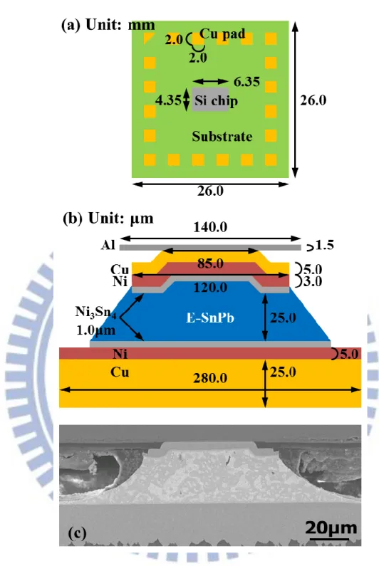
To reduce cost, the chip-on-substrate technology was employed to fabricate the flip-chip solder bump samples, as shown in Figure 2-1 (a). The Si chip was 6.35 mm × 4.35 mm × 0.3 mm, while that of the FR4 substrate was 26.0 mm × 26.0 mm × 1.0 mm. A total of 34 flip-chip solder bumps were made in the Si chip using lithography process, but only four of them were designed as Kelvin bump structures for measuring the bump resistance. The pitch between bumps was 800 μm. After the flip and the proper alignment between the chip and the substrate, the chip was bonded onto the substrate by 1-min reflow. After that, the underfill was heated to 75ºC to increase the fluidity, injected into the space between those solder bumps, and then fixed it by cooling it down to room temperature.
-30-
On the Si chip were 1.5-μm thick Al traces deposited by sputtering. The width of the Al traces was 100.0 μm, and the diameter of the Al pad was 140.0 μm. The diameter of the passivation opening and the UBM opening were 85.0 μm and 120.0 μm respectively. On the sputtered Ti/Cu seed layer (3000 Å in thickness), the 5.0-μm Cu/ 3.0-μm Ni UBM was electroplated. Because the passivation opening was confined by a 3.0-μm thick polyimide layer, the shape of the UBM looked like a cap. The eutectic SnPb (E-SnPb) solder was electroplated as well; after the electroplating, the solder was reflowed for 1 min. The reflow caused the formation of the intermetallic compound (IMC), Ni3Sn4, which is a chemical attachment and enhances the bonding
between UBM and E-SnPb solder. Next, the entire structure was flipped upside-down and reflowed for 1 min to construct the bonding between the solder and the metallization on the substrate, which was electroplated 25.0-μm Cu/5.0-μm Ni. The IMC on the surface of substrate metallization was 1.0-μm Ni3Sn4, and the diameter of
the substrate metallization is 280.0 μm. It was much larger than that of the UBM opening (120.0 μm) and caused the solder to spread out, thus forming a solder of very low height. The height of solder is only 25.0 μm. The 100.0-μm wide traces on the substrate and the pads were made using Cu.
The cross-sectional scanning electron microscope (SEM) image of the flip-chip solder bump is shown in Figure 2-1 (c). As can be seen, the bump was well aligned and the Pb-rich phase dispersed uniformly in the Sn matrix. Moreover, there was no void found in the solder. The fabrication process was very stable.
-31-
Figure 2-1 (a) Schematic illustration in plan-view of an entire flip-chip sample; (b) schematic illustration of the flip-chip solder bump; and (c) cross-sectional SEM image of a flip-chip solder bump.
-32-
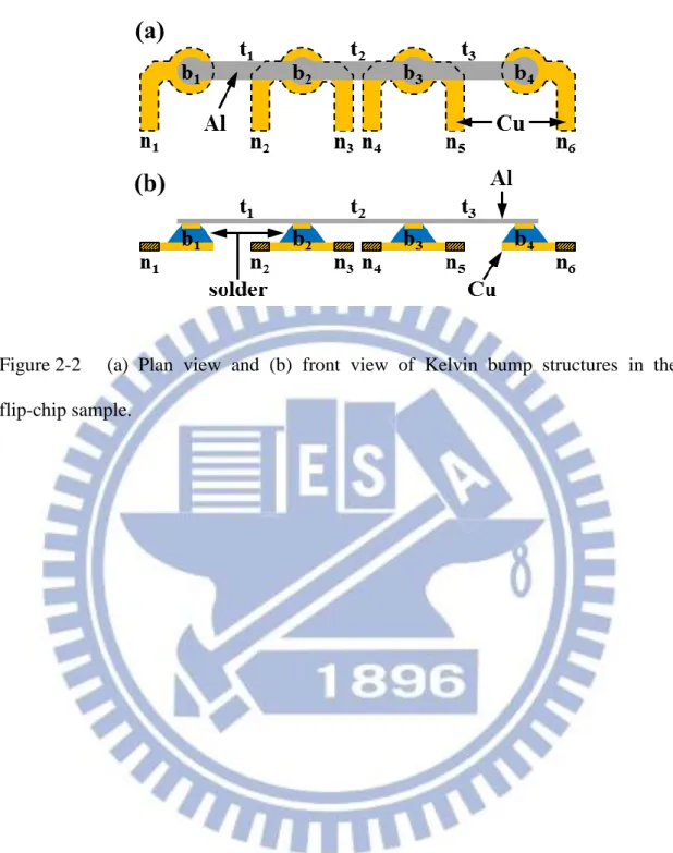
2.1.2. Kelvin Bump Structures and Experimental Procedures
In order to measure the bump resistance of a single bump, a Kelvin bump structure is necessary. As mentioned in section 2.1.1, only four of the bumps were designed as Kelvin bump structures, which are shown in Figure 2-2. Figure 2-2 (a) shows the plan view of the Kelvin bump structures while Figure 2-2 (b) shows the front-side cross-sectional view. In this figure, the gray-colored region indicat the Al traces and pads on the Si chip; the yellow-colored regions within black dashed lines indicate the Cu traces and pads on the substrate; and the four bumps between Al pads and Cu pads were marked b1 to b4. On the one hand, there were three Al traces,
marked as t1, t2, and t3, placed between the bumps to connect them. On the other hand,
six Cu traces marked n1, n2 … to n6 were also connected to those four bumps. With
this setup of Kelvin bump structures, the resistance of b2, b3, and t2 can be obtaied.
In Kelvin bump structures, if n3 and n4 are connected to the negative end and the
positive end of a DC source respectively, the current will flow through the following paths: n4, b3, t2, b2, and n3. The bump resistance of b2 and b3 can be obtained by
measuring the voltage drop across b2 and b3. The bump resistance equals the value of
voltage drop over the applied current. In this circumstance, the electron flows upward (from the substrate to the Si chip) in b2 and downward (from the Si chip to the
substrate) in b3. Therefore, the bump resistance of the bumps with both upward and
downward electron flow can be monitored at the same time, and so can the resistance of the entire circuit and t2. The detailed measurement setup is shown in Table 2-1.
When the current was applied from n4 to n3, the voltage drop across b3 can be
obtained from n5 and n6; the one across b2 can be obtained from n1 and n2; and the one
across t2 can be obtained from n6 and n1. In this study, all the resistance of b2, b3, and
-33-
The tests were performed on a 150ºC hot plate. The applied current was 0.8 A, and the corresponding current density were 7.1 × 10³ A/cm2. Although the resistance of b2, b3, and t2 were all monitored during the tests, only the bump resistance of b3
was analyzed in detail and discussed in this study since the flip-chip bump loaded by downward electron flow was usually the weakest spot in the entire structure. [13, 16, 31, 70, 73-74] Testing would continue until the bump resistance of b3 reached 1.03, 1.10, 1.20, 1.50, and 10.0 times that of the initial resistance value. Those samples reaching the above specific bump resistance values were marked as stages 1, 2, 3, 4, and 5, respectively. Moreover, the initial sample without current stressing was marked as stage 0 or initial stage, and the sample behaving as a fully open circuit was called the final stage.
After testing, the samples were first scanned by a two-dimensional X-ray imaging system to roughly observe the distribution of voids caused by current stressing. Next, the sample of different stages were carefully polished to the central cross-section of the tested bumps, and then observed by SEM. The composition of IMC was confirmed by energy dispersive X-ray spectrometer (EDX). Finally, the growth rate of void at different stages was also analyzed.
-34-
Figure 2-2 (a) Plan view and (b) front view of Kelvin bump structures in the flip-chip sample.
-35-
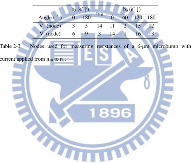
Voltage
drop Direction of electron flow
Measurement nodes
High voltage Low voltage
∆Vtotal n3-b2-t2-b3-n4 n4 n3
∆Vb2 upward (substrate to chip) n1 n2
∆Vb3 downward (chip to substrate) n5 n6
∆Vt2 from b2 to b3 n6 n1
Table 2-1 Nodes used for measuring bump resistances of a flip-chip bump with current applied from n4 to n3.
Stage Bump resistance of b3
0 (or Initial) Ri 1 1.03 × Ri 2 1.10 × Ri 3 1.20 × Ri 4 1.50 × Ri 5 10.00 × Ri Final Open
Ri: the initial bump resistance of b3


![Figure 1-6 SEM images of void formation and propagation in a flip-chip E-SnPb solder bump stressed at 125ºC by 2.25 × 10 4 A/cm 2 for (a) 38 hr, (b) 40 hr, and (c) 43 hr [16]; and (d) SEM image of void formation in a flip-chip 95.5Sn4.0Ag0.5](https://thumb-ap.123doks.com/thumbv2/9libinfo/8109963.165508/34.892.136.678.101.865/figure-images-formation-propagation-snpb-solder-stressed-formation.webp)
![Figure 1-8 Top region of a solder bump after current stressing of 1.6 × 10 4 A/cm 2 at 150ºC for (a) 30 min, (b) 60 min, (c) 100 min, and (d) 120 min [53]; (e) melted solder joint due to large Joule heating before an open circuit [53]; and](https://thumb-ap.123doks.com/thumbv2/9libinfo/8109963.165508/36.892.140.679.99.958/figure-solder-current-stressing-melted-joule-heating-circuit.webp)