phys. stat. sol. (c) 2, No. 7, 2377 – 2380 (2005) / DOI 10.1002/pssc.200461496
© 2005 WILEY-VCH Verlag GmbH & Co. KGaA, Weinheim
Recombination mechanism of InGaN multiple quantum wells
grown by metalorganic chemical vapor deposition
Z. C. Feng*,1 , W. Liu2 , S. J. Chua2 , J. H. Chen1 , C. C. Yang1 , W. Lu3 , and W. E. Collins3 1
Graduate Institute of Electro-Optical Engineering & Department of Electrical Engineering, National Taiwan University, Taipei, 106-17 Taiwan
2
Institute of Materials Research & Engineering, 3 Research Link, Singapore 117602
3
Department of Physics, Fisk University, Nashville, TN 37208, USA Received 12 July 2004, revised 26 September 2004, accepted 8 February 2005 Published online 24 March 2005
PACS 68.65.Fg, 78.55.Cr, 78.67.De, 81.15.Gh
A series of InGaN/GaN multiple quantum wells with different well thicknesses were grown on sapphire by metal organic chemical vapor deposition, and investigated by excitation power density dependent pho-toluminescence (PL). With increasing excitation power density, the PL peak position showed a blue shift followed by a red shift. It is believed that a screened quantum-confined Stark effect is responsible for the blue shift and the band gap renormalization due to the many body effect is responsible for the red shift.
© 2005 WILEY-VCH Verlag GmbH & Co. KGaA, Weinheim
1 Introduction
Tremendous progresses in the GaN-based materials and devices for optoelectronic and electronic appli-cations have been made recently. InGaN-based light emitting diodes (LED) and laser diodes (LD) grown on sapphire are now available commercially [1, 2]. InGaN/GaN multiple quantum wells (MQWs) are attracting much research interest currently, acting as the active layer in above high brightness III-Nitride light emitting diode (LED) and cw blue-green laser diode (LD) [1, 3, 4]. InGaN/GaN heterostructures can exhibit intense photoluminescence (PL) and electroluminescence (EL) despite of a high dislocation and defects density existed [5,6], and have advantages, such as, lowering the threshold current density for LDs and reducing the device sensitivity to temperature [7, 8].
However, many fundamental scientific and technological issues, related to the growth of high-quality InGaN MQWs, are still unclear. For example, there exist different opinions or models on the recombina-tion mechanism of InGaN MQWs, such as localized excitons [9], quantum dot (QD) – like structures [10, 11], band-filling in localized states [12, 13], strain-induced piezoelectric field and quantum-confined Stark effect (QCSE) [14, 15]. In this study, a series of InGaN/GaN MQWs with 3-periods but different well thicknesses were grown on sapphire by metalorganic chemical vapor deposition (MOCVD) and studied by excitation power density dependent PL. The PL mechanisms in MQWs are discussed, based upon a unique blue-red shift behavior at different excitation power density levels.
2 Experimental
High quality InGaN MQWs were grown on (0001)-plane sapphire substrates by low pressure (LP) MOCVD. Trimethylgallium (TMGa), Trimethylindium (TMIn), and ammonia NH3 were used as
precur-sors. The carrier gas was H2 and N2, respectively, for the growth of GaN and InGaN. In this study, four
*
2378 Z. C. Feng et al.: Recombination mechanism of InGaN multiple quantum wells
© 2005 WILEY-VCH Verlag GmbH & Co. KGaA, Weinheim
experimental samples were investigated, in which the structures were: (0001) sapphire, 30 nm low tem-perature (520o
C) grown GaN, 1000 nm thick high temperature (HT) (1020 o
C) grown GaN, 3-period InGaN MQWs grown at 800 o
C, and 20 nm HT-grown GaN cap. The barrier material in MQWs was InGaN with a x(In)= 0.03 and a thickness of 50 Å for all samples. The well was InGaN of x(In) = 0.13 with thickness of 25, 30, 45 and 60 Å, respectively. A Philips MRD high resolution (HR) X-ray diffrac-tion (XRD) including a five-crystal monochromator and a Renishaw micro-PL system equipped with a 325 nm He-Cd laser were used for characterization, measured at room temperature (RT). The excitation power on the sample was varied using a neutral density filter in the excitation light path.
3 Results
3.1 High resolution X-ray diffraction
Experimental InGaN MQWs were characterized by HR-XRD 2θ-ω scan at (0006) configuration. Figure 1 shows a typical pattern for an InGaN MQW sample with a well thickness of 25 Å and the barrier thick-ness of 50 Å. The satellite peaks from MQW structure are observed even though only 3 periods were grown (here only 0th and -1st order peaks are exhibited). The full width at half maximum (FWHM) value of the InGaN 0th peak is 9.1 arc-minutes. These results indicate the high quality of the epilayers and the abrupt QW interfaces, for only 3-well structures. All other samples also show similar HR-XRD patterns. 120 122 124 126 128 130 132 1 10 100 1000 (0006) 2θ (Degree) InGaN MQWs -1th 0th GaN XRD I nt ens ity ( C ount s)
Fig. 1 X-ray diffraction (0006) pattern of an InGaN MQW with d(well) = 25 Å and d(barrier) = 50 Å.
350 400 450 500 Iexc=40 W/cm2 T=300 K FWHM=14 nm (104meV) GaN InGaN MQWs 404.9 nm Lw=2.5 nm Lb=5.0 nm PL In te ns ity (a .u .) Wavelength (nm)
phys. stat. sol. (c) 2, No. 7 (2005) / www.pss-c.com 2379
© 2005 WILEY-VCH Verlag GmbH & Co. KGaA, Weinheim
3.2 Photoluminescence
Room temperature PL was measured on the four samples. Figure 2 shows a RT PL spectrum for the InGaN MQW sample with the well thickness of 25 Å and barrier thickness of 50 Å at excitation level of 40 W/cm2
. A strong PL emission band is observed at 405 nm, which comes from the InGaN MQW struc-ture. Its intensity is much stronger compared to that from the underlying GaN layer. The FWHM value of this major emission band is 104 meV only (14 nm in terms of wavelength). The results for other samples are similar to the spectrum in Figure 2 except with different peak positions and slightly different FWHMs which are not shown here. These results indicate the high optical quality of the samples.
3.3 Dependence of the PL peak energy on the excitation power
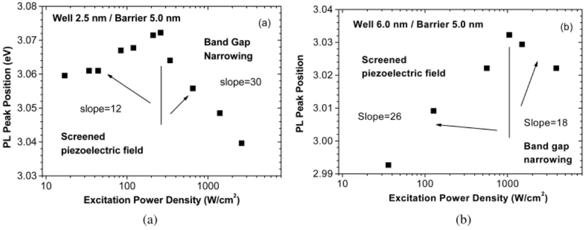
It is observed that the PL spectra of these InGaN MQWs are varied with the excitation power density. RT excitation-intensity dependent PL measurements were performed on two samples with the narrowest 25 Å and widest 60 Å well thickness, respectively. Their peak energy positions are plotted as a function of the excitation power density in Figs. 3 (a) and (b), respectively. Two samples show similar trends. At first, the major MQW PL peak is blue-shifted as the excitation power density is increased. After reaching a maximum, the PL peak is converted to shift towards red as the excitation power density increases fur-ther. The increasing slope for the narrower-well sample is smaller than that of wider-well sample, while the decreasing slope for the narrower-well sample is larger than that of the wider-well sample. To our knowledge, this interesting phenomenon has not been observed in the literature yet.
10 100 1000 3.03 3.04 3.05 3.06 3.07 3.08 (a) slope=30 slope=12 Well 2.5 nm / Barrier 5.0 nm Band Gap Narrowing Screened piezoelectric field PL Peak Posi tion ( eV)
Excitation Power Density (W/cm2)
10 100 1000 2.99 3.00 3.01 3.02 3.03 3.04 (b) Slope=18 Slope=26 Well 6.0 nm / Barrier 5.0 nm Band gap narrowing Screened piezoelectric field PL Peak Position
Excitation Power Density (W/cm2)
(a) (b)
Fig. 3 Dependence of PL peak energy position on PL excitation power density for InGaN MQWs of (a) d(well) = 25 Å and d(barrier) = 50 Å, and (b) d(well) = 60 Å and d(barrier) = 50 Å.
4 Discussion
Recently, Kuokstis et al. [13] and Gotoh et al. [8] have reported the PL blue shift from InGaN MQWs, but both studies did not observe red-shift. Our experiments have revealed a different interesting behavior of the InGaN MQW PL peak position, which is dependent upon the excitation power level with blue-red shift. A primary qualitative explanation can be given as follows: it is well known that InGaN MQWs are subject to strain due to the mismatch of lattice constants and the difference in thermal expansion coeffi-cients between InGaN and GaN. This strain causes a piezoelectric field existing in the wells, and thus induces the so-called quantum confined Stark effect (QCSE). It means that the QW PL transition energy becomes smaller in this case compared to the case of no strain and thus no electric field.
When the laser light excites the MQWs, photo-generated carriers are accumulated at the opposite side of the well due to the electric field and in turn screen this electric field. It causes an increase of the transi-tion energy, i.e. a blue shift of the PL peak. The blue-shift magnitude of the wider-well sample is much larger than that of the narrower-well sample. This is also an indication of the screened QCSE effect since QCSE is more significant in wider well samples.
2380 Z. C. Feng et al.: Recombination mechanism of InGaN multiple quantum wells
© 2005 WILEY-VCH Verlag GmbH & Co. KGaA, Weinheim
As the excitation power is strong enough, the piezoelectric field might be screened completely, causing the flattening of the energy level in the well. In this case, the transition energy in the quantum well will reach a maximum and the PL peak is not blue-shifted any more as the excitation power increases further.
However, as the photo-generated carriers are further accumulated in the well, many body interactions may take place, leading to the shrinkage of the band gap, i.e. the band renormalization. The band gap narrowing, ∆Εg, due to the energy band normalization is proportional to n
1/3
where n is the carrier tration [16]. In PL experiments, the carriers come from photon-injection and therefore the carrier concen-tration is proportional to the excitation light intensity, I, assuming the quantum efficiency equal to 1. Therefore, we have ∆Εg ∝ n
1/3
∝ I1/3
. This relationship is believed to be a coincidence with the data in Fig. 3, where the semi-log plots show the linearity of the data points. This demonstrates that the band gap is reduced with the excitation light intensity as shown in Fig. 3 which is resulted by the energy band renormalization.
It is also noted that the red-shift magnitude of the narrower-well sample is larger than that of the wi-der-well sample. This is because the density of states of narrower well is smaller and the many body effect is more significant, compared to the case of wider well. Further penetrating investigation on this interesting effect is under way both in further experiments and theoretical calculations.
5 Conclusion
Excitation power density dependent PL measurements are performed on a series of MOCVD-grown InGaN MQWs samples (on sapphire substrates) with different well thicknesses. A blue shift in the PL peak position is shown when the excitation power density increases, and a blue shift appears as further increasing the excitation power density. This unique phenomenon suggests that a screened quantum confined Stark effect (QCSE) is responsible for the blue shift and the band gap renormalization is re-sponsible for the red shift due to the many body effect.
References
[1] S. Nakamura, S. Pearton, and G. Fasol, The Blue Laser Diode – The Complete Story (Springer, Berlin, 2000). [2] E. T. Yu and O. Manasreh (Eds.), 2003 III-V Nitride Semiconductors: Applications & Devices, Vol. 16, in:
O. Manasreh (Ed.), Optoelectronic Properties of Semiconductors and Superlattices (New York, Taylor & Fran-cis).
[3] S. Nakamura, M. Senoh, S. Nagahama, N. Iwasa, T. Yamada, T. Matsushita, H. Kiyoku, Y. Sugimoto, T. Kozaki, H. Umemoto, M. Sano, and K. Chocho, Appl. Phys. Lett. 72, 2014 (1998).
[4] J. J. Song and W. Shan, in: Gallium Nitride and Related Semiconductors, ed. B. Gil (Michael Faraday House, London, 1999), p. 596.
[5] S. Nakamura, M. Senoh, S. Nagahama, N. Iwasa, T. Yamada, and T. Nukai, Appl. Phys. Lett. 68, 3286 (1996); 69, 1477, 4056 (1996).
[6] K. S. Ramaiah, Y. K. Su, S. J. Vhang, B. Kerr, H. P. Liu, and L. G. Chen, Appl. Phys. Lett. 84, 3307 (2004). [7] M. Koike, S. Yamasaki, S. Nagai, N. Koide, S. Asami, H. Amano, and I. Akasaki, Appl. Phys. Lett. 68, 1403
(1996).
[8] H. Gotoh, T. Tawara, Y. Kobayashi, N. Kobayashi, and T. Saitoh, Appl. Phys. Lett. 83, 4791 (2003). [9] S. Chichbu, T. Azuhata, T. Sota, and S. Nakamura, Appl. Phys. Lett. 69, 4188 (1996).
[10] Y. Narukawa, Y. Kawakami, M. Funato, Sz. Fujita, Sg. Fujita, and S. Nakamura, Appl. Phys. Lett. 70, 981 (1997).
[11] S. W. Feng, Y. C. Cheng, Y. Y. Chung, C. C. Yang, M. H. Mao, Y. S. Lin, K. J. Ma, and J. I. Chyi, Appl. Phys. Lett. 80, 4375 (2002).
[12] Y.-H. Cho, J. J. Song, S. Keller, U. K. Mishra, and S. P. DenBaars, Appl. Phys. Lett. 73, 3181 (1998). [13] E. Kuokstis, J. W. Yang, G. Simin, M. A. Khan, P. Gaska, and M. S. Shur, Appl. Phys. Lett. 80, 977 (2002). [14] T. Takeuchi, H. Amano, and I. Akasaki, Jpn. J. Appl. Phys. 39, 413 (2000).
[15] C. H. Chen, W. H. Chen, Y. F. Chen, and T. Y. Lin, Appl. Phys. Lett. 83, 1770 (2003). [16] X. Zhang, S. J. Chua, W. Liu, and K. B. Chong, Appl. Phys. Lett. 72, 1890 (1998).