596 IEEE ELECTRON DEVICE LETTERS, VOL. 28, NO. 7, JULY 2007
Transport Mechanism of SiGe Dot MOS
Tunneling Diodes
P.-S. Kuo, C.-H. Lin, C.-Y. Peng, Y.-C. Fu, and C. W. Liu, Senior Member, IEEE
Abstract—The blockage of hole transport due to excess holes in
SiGe dots was observed in the MOS tunneling diodes for the first time. The five layers of self-assembled SiGe dots are separated by 74-nm Si spacers and capped with a 130-nm Si. The hole tunneling current from Pt gate electrode to p-type Si dominates the inversion current at positive gate bias and is seven orders of magnitude higher than the Al gate/oxide/p-Si device. The large work function of Pt is responsible for the hole transport current from Pt to p-Si. The incorporation of SiGe dots confines the excess holes in the valence band and forms a repulsive barrier to reduce the hole transport current from Pt to SiGe dots by 2–3 orders of magnitude in comparison with the Pt/oxide/p-Si device. This repulsive barrier also reduces the hole tunneling current from SiGe dots to Pt at negative gate bias.
Index Terms—MOS tunneling diode, repulsive barrier, SiGe
dots, transport mechanism.
I. INTRODUCTION
T
HE METAL OXIDE Si tunneling diodes have been used as light emitters [1] and photodetectors [2]. To tune the emission wavelength of LEDs [3] and to extend the cutoff wavelength of photodetectors [4], the SiGe layer is inserted in the Si. Optical, physical, and material properties of Si/Ge dots were reported [5] [6]. Moreover, the current transport of a MOS diode is significantly influenced by these SiGe layers. Therefore, MOS diodes with the Pt (5.65 eV) and Al (4.1 eV) gates with SiGe dots are studied, and a new transport mecha-nism is proposed in this letter.II. DEVICEFABRICATION
The low-temperature liquid-phase-deposited (LPD) SiO2 of 2.5 nm (ellipsometry) was deposited on both the p-type SiGe dot structure and the control p-type Si. The desired Ge dots were grown by ultrahigh vacuum chemical vapor deposition (UHVCVD) on p-type (001) substrates with the resistivity of 15–25 Ω · cm. Due to Si/Ge interdiffusion at 600◦C, the Ge dots transformed into SiGe dots. The top and bottom SiGe dots, including the wetting layers, have about 2× 10¹⁶ and 1.5× 10¹⁶ Ge atoms/cm2, respectively. The lower density of the bottom layer is due to the extra thermal budget after the bottom dots are grown. The SiGe layers are separated by
Manuscript received March 19, 2007; revised April 12, 2007. This work was supported by the National Science Council, Taiwan, R.O.C., under Contracts 95-2221-E-002-357 and 95-2221-E-002-370. The review of this letter was arranged by Editor E. Sangiorgi.
The authors are with the Department of Electrical Engineering and Graduate Institute of Electronics Engineering, National Taiwan University, Taipei 10617, Taiwan, R.O.C. (e-mail: [email protected]).
Digital Object Identifier 10.1109/LED.2007.898288
Fig. 1. (a) Structure of five-layer SiGe dot MOS diodes. (b) TEM micrograph of SiGe dot samples grown by UHVCVD.
74-nm Si spacer layers. A 130-nm Si cap was deposited on the top layer of the self-assembled SiGe dots. The SiGe dots in the top layer consist of a structure with a ∼100-nm base and a∼7-nm height, with standard deviations of 13 and 3 nm, respectively. Fig. 1 shows the schematic structure and the TEM micrograph of the five-layer SiGe dots in this letter.
III. RESULTS ANDDISCUSSION
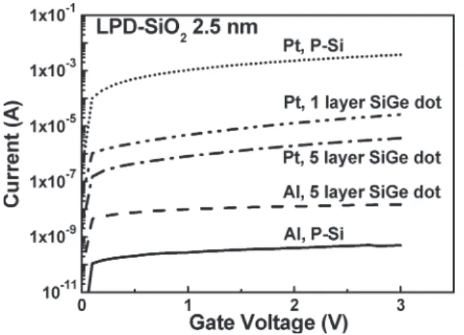
Due to the high density of traps in LPD oxide, the tun-neling current is dominated by trap-assistant tuntun-neling [7]. The different SiGe/Si structures have different magnitudes of current, indicating that SiGe dots play the key role in the transport mechanism and LPD oxide is not crucial. For the Pt electrode at positive gate bias, the inversion currents of single-layer and five-layer SiGe dot devices are two and three orders of magnitude smaller than that of control Si devices, respectively. However, for the Al gate electrode, five-layer SiGe dot device has an inversion current higher than the control Si device (Fig. 2).
Fig. 3(a) shows the band diagram of the SiGe dot devices at positive gate bias (inversion). At positive gate bias, the semi-conductor is deeply depleted, and the oxide voltage is small. The large hole barrier height (5.85 eV) of the Al gate prevents the hole tunneling from Al to the semiconductor. Therefore, the thermally generated electrons via the oxide/Si interface traps and the bulk traps in the depletion region dominate the gate current [8]. Due to the smaller bandgap of SiGe dots compared to Si, the SiGe dot device yields a larger current. Note that due to the thin LPD oxide (2.5 nm) and traps in the LPD oxide, the electron tunneling (voltage dependent) through the oxide is the faster process as compared to the thermal generation process (weak voltage dependence). Therefore, the current of
0741-3106/$25.00 © 2007 IEEE
KUO et al.: TRANSPORT MECHANISM OF SiGe DOT MOS TUNNELING DIODES 597
Fig. 2. I–V characteristics of Pt gate and Al gate devices at positive gate bias (∼inversion). The die area is 5E − 3 cm2.
Fig. 3. Band diagrams of the NMOS SiGe dot device with Pt or Al gate operated at (a) positive gate bias (∼inversion) and (b) negative gate bias (∼accumulation).
Al gate devices at positive gate bias is dominated by thermally generated electrons. However, for Pt devices, the hole barrier is 4.3 eV, and the hole tunneling current from Pt to semiconductor is significantly larger than the electron generation current. As a result, the inversion current of the Pt-gate Si device is seven orders larger than the Al-gate Si device (Fig. 2) due to the ad-ditional hole tunneling current from the Pt gate electrode to the semiconductor. The repulsive barrier at the valence band due to the trapped holes in the SiGe dots blocks the hole transport and reduces the inversion current for the Pt device with SiGe dots. To confirm the hole blocking effect, the current at negative gate bias is also studied. For the Pt gate device at negative gate bias, the electron barrier from Pt to semiconductor is similar to the hole barrier from semiconductor to Pt (4.7 eV) [Fig. 3(b)] for both control Si and SiGe devices. The electron current tunneling from Pt to semiconductor is limited by a diffusion in p-type semiconductor, and the hole tunneling current from semiconductor to Pt can reach the contact rapidly by relaxation process in metal. As a result, the hole current is dominant at negative gate bias for the Pt device. The repulsive barrier due to the confined holes in SiGe dots blocks the hole tunneling current. Therefore, for the Pt gate, the five-layer SiGe dot device has a lower current than the Si device at the negative gate bias (Fig. 4). Note that the SiGe dots referred to in this letter include a wetting layer. The Pt gate device with a 3-nm Si cap and
Fig. 4. Low-temperature and room-temperatureI–V of the Si and five-layer SiGe dot devices with Pt gate electrode at the negative gate bias. The die area is 5E− 3 cm2. The results of Al gate devices are shown in the inset.
Fig. 5. Simulated band diagrams of the five-layer SiGe well device and the control Si device with Pt gate operated at−4 V at 40 K. The SiGe quantum wells have the thickness of 5 nm and are separated by 74-nm Si spacers. The Si cap is 130 nm. The oxide thickness is 2.5 nm and is not scaled in the figure.
single SiGe well also has a lower current than the control Si device at both the positive and negative gate biases. The low work function Al (4.1 eV) and high work function Pt (5.65 eV) are investigated as gate electrodes to evaluate the transport mechanism of MOS tunneling diodes. Other high work function metals such as Au (5.15 eV) and ALD-TiN (5.3 eV) and low work function metals such as Ti (4.3 eV) and Ta (4.3 eV) should have similar results if Fermi level pinning does not exist. Actually, the interface states at the metal/oxide interface may cause the Fermi level pinning to some extent, which reduces the work function difference between Pt and Al. Therefore, the difference in characteristics between Al and Pt gate devices should be less significant if Fermi level pinning occurs. In addition, thermal treatment and process conditions can also affect the work function and should be taken into account for the device design using the hole blocking effect.
The low-temperature (40 K) I–V measurement at negative gate bias is also shown in Fig. 4. Fig. 5 shows the energy band diagrams simulated by the commercial tool [9] for the Pt devices with five layers of 5-nm Si0.46Ge0.54 quantum wells as well as for the control Si device at−4 V at 40 K. At low temperature, more holes are confined in the SiGe quantum
598 IEEE ELECTRON DEVICE LETTERS, VOL. 28, NO. 7, JULY 2007
wells, and there is an additional voltage across the 130-nm Si cap, while for the Si MOS device, most voltage drop is across the oxide. For the five-layer SiGe dot device at the small negative gate bias (|Vg| < 4 V), the Fermi level of Pt does not exceed the conduction band edge of semiconductor at the SiO2/semiconductor interface due to a large voltage drop across the Si cap. Therefore, the electrons in Pt are not allowed to tunnel to the substrate, and hole tunneling current from the substrate to Pt is dominant. When the negative gate bias increases, the Fermi level of Pt is above the conduction band edge of the semiconductor at the interface, and the electrons in Pt can tunnel to the substrate (Fig. 5). Therefore, the kink at∼ − 4 V in the I–V curve of the Pt-gate SiGe dot device at 40 K is due to the onset of the electron current tunneling from Pt to semiconductor. At low temperature, due to the more abrupt transition of the Fermi–Dirac distribution, there are more holes trapped in SiGe dots. Therefore, the hole blocking effect is more significant, and the current of the Pt-SiGe dot device is smaller at 40 K than at room temperature. The quantum mechanism simulation shows that the hole concentration(9.3 × 1017cm−3) at 40 K is 1.6 times of that (6 × 1017cm−3) at room temperature at−1 V in the quantum wells using the commercial tool [9]. The lower hole density in the wells at room temperature also reduces the voltage across the Si cap and increases the electron tunneling current from Pt to semiconductor. However, for Al-gate devices at negative gate bias, due to the much smaller electron barrier (3.1 eV) compared to the hole barrier (4.7 eV), the electron current is dominant, and the electrons tunneling from the Al electrode are limited by the diffusion process (temperature dependent) in the p-type semiconductor. At 300 K, the current of the SiGe dot device is similar to that of the Si device (Fig. 4 inset) due to electron current not being lowered by the repulsive barrier in the valence band. However, at 40 K, the current decrease of both the SiGe dot device and the Si device compared to that at 300 K is not due to the repulsive barrier, but due to the temperature-dependent electron diffusion.
IV. CONCLUSION
The transport mechanisms in SiGe dot MOS devices with Al and Pt gates are investigated. The valence band offset in Si/SiGe heterojunction can confine holes and forms a repulsive energy barrier to block the hole current. In view of its application, the supply of holes from Pt into SiGe dots can be designed for the intraband transition in far infrared photodetectors [10].
ACKNOWLEDGMENT
The authors would like to thank Hung for the English improvement.
REFERENCES
[1] C. W. Liu, M. H. Lee, M.-J. Chen, I. C. Lin, and C.-F. Lin, “Room-temperature electroluminescence from electron-hole plasmas in the meta-oxide-silicon tunneling diodes,” Appl. Phys. Lett., vol. 76, no. 12, pp. 1516–1518, 2000.
[2] C. W. Liu, W. T. Liu, M. H. Lee, W. S. Kuo, and B. C. Hsu, “A novel photodetector using MOS tunneling structures,” IEEE Electron Device
Lett., vol. 21, no. 6, pp. 307–309, Jun. 2000.
[3] M. H. Liao, C.-Y. Yu, T.-H. Guo, C.-H. Lin, and C. W. Liu, “Electro-luminescence from the Ge quantum dot MOS tunneling diodes,” IEEE
Electron Device Lett., vol. 27, no. 4, pp. 252–254, Apr. 2006.
[4] B.-C. Hsu, S. T. Chang, T.-C. Chen, P.-S. Kuo, P. S. Chen, Z. Pei, and C. W. Liu, “A high efficient 820 nm MOS Ge quantum dot photodetector,”
IEEE Electron Device Lett., vol. 24, no. 5, pp. 318–320, May 2003.
[5] O. G. Schmidt and K. Eberl, “Multiple layers of self-assembled Ge/Si islands: Photoluminescence, strain fields, material interdiffusion, and island formation,” Phys. Rev. B, Condens. Matter, vol. 61, no. 20, pp. 13 721–13 729, 2000.
[6] G. Schmidt and K. Eberl, “Strain and band-edge alignment in single and multiple layers of self-assembled Ge/Si and GeSi/Si islands,” Phys. Rev.
B, Condens. Matter, vol. 62, no. 24, pp. 16 715–16 720, 2000.
[7] B.-C. Hsu, W.-C. Hua, C.-R. Shie, K.-F. Chen, and C. W. Liu, “Growth and electrical characteristics of liquid-phase deposited SiO2 on Ge,”
Electrochem. Solid-State Lett., vol. 6, no. 2, pp. F9–F11, 2003.
[8] C.-H. Lin, B.-C. Hsu, M. H. Lee, and C. W. Liu, “A comprehensive study of inversion current in MOS tunneling diodes,” IEEE Trans. Electron
Devices, vol. 48, no. 9, pp. 2125–2130, Sep. 2001.
[9] Synopsys Sentaurus Tcad Simulator.
[10] C.-H. Lin, C.-Y. Yu, P.-S. Kuo, C.-C. Chang, T.-H. Guo, and C. W. Liu, “Delta-doped MOS Ge/Si quantum dot/well infrared photodetector,” Thin
Solid Films, vol. 508, no. 1–2, pp. 389–392, 2006.