A 9-GHz QUADRATURE-PHASE VCO IN 0.18-
μ
m CMOS
9-GHz 正交壓控震盪器
摘 要 本論文中將實現一個9-GHz 的正交壓控震盪器。根據 量測所得,以切換式偏壓的改良式電流源可以降低相位雜 訊的大小;同時,所採用的二進位式切換電容,能夠有效 的提高可調頻率範圍。使用CMOS 0.18-μm 製程,在 2-V 的供給電壓之下,整個電路所消耗的功率大小為24 mW; 最高工作頻率為 9-GHz;可調範圍為 16%;距輸出頻率 1-MHz 所量測到的相位雜訊為−99.48 dBc/Hz。 關鍵詞:正交相位、壓控震盪器。Abstract
A fully integrated 9-GHz quadrature-phase VCO based on two cross-coupled LC-tank VCOs is presented. Switched-bias technique is employed for phase noise reduction while varactors with binary-weighted capacitor arrays are used to increase the frequency tuning-range. Implemented in a 0.18-μm CMOS technology, the quadrature-phase VCO core consumes a dc power of 24 mW from a 2-V supply voltage. The maximum output frequency is 9 GHz with 16% frequency tuning-range. The measured phase noise is−99.48 dBc/Hz at 1-MHz offset frequency.
Keywords: voltage controlled oscillator, quadrature
phase, CMOS oscillator, frequency tuning range, phase noise, switched-bias technique, flicker noise.
1. INTRODUCTION
The rapid growth of optical communication markets has motivated the development of high data-rate transceivers. Due to the speed requirement, III-V compound semiconductors have been widely used for the circuit implementation. With recent advances in fabrication technology, transistors with fT and fmax
beyond 100 GHz [1~5] are available in standard CMOS processes, providing a promising solution to low-cost implementation of high-speed integrated circuits. As a result, research on CMOS circuits for multiple giga-bit applications has attracted great attention recently.
In a high data-rate transceiver system, quadrature- phase VCO is frequently used for clock and data
recovery (CDR)[6]. As the data-rate increases, VCO circuits operate at higher frequencies are required. Due to the limitations imposed on both active and passive devices in the CMOS technology, typical high-frequency VCO designs suffer from significant degradation in circuit performance, such as phase noise, frequency tuning-range and output power.
In this paper, a fully integrated quadrature-phase VCO using a standard 0.18-μm CMOS process is proposed to operate at 9-GHz frequency band. The VCO design is composed of two LC-tank VCOs with active coupling pairs to generate the quadrature-phase at the output. By adopting switched-bias technology and binary-weighted capacitor arrays, the fabricated VCO demonstrates low phase noise while maintaining a wide tuning-range around 9 GHz.
Ying-Chih Hsu* Liang-Hung Lu**
徐
英 智
呂
良 鴻
*
M.S. student **Assistant Professor Graduate Institute of Electronics Engineering, National Taiwan University, Taipei, Taiwan 10617, R.O.C.
*
碩士班研究生 **助理教授
The paper is organized as follows. Section II describes the circuit design of the quadrature-phase VCO. The experimental results are presented in Section III. Conclusions are finally given in Section IV.
2. CIRCUIT DESIGN
2.1 Design of the Cross-Coupled VCO
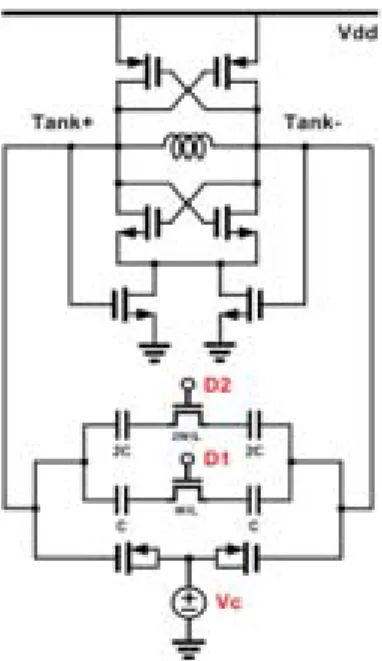
Figure 1 shows the schematic of the proposed cross-coupled LC-tank VCO. The LC-tank consists of a differential spiral inductor, accumulation-mode MOS varactors, and two-bit binary-weighted MIM capacitor array to achieve a high quality factor and a wide frequency tuning-range. Complementary cross- coupled pairs serve as the negative resistance to compensate for the energy losses from the LC-tank. Compared with VCO topologies with single cross- coupled pair, the complementary architecture provides a higher transconduct-ance at the same bias current. In addition, a more symmetric oscillating waveform can be obtained at the output, resulting in a reduction in the up-conversion of 1/f noise with low-frequency noise sources [7].
According to the analysis in [8], the close-in phase noise of a CMOS VCO is largely determined by the flicker noise of the tail current sources. In a conventional VCO topology, a fixed tail current is used to provide the bias current of the cross-coupled pairs. The flicker noise generated by the current source is up-convertedto theskirt ofthe outputspectrum of the
Fig. 1 The schematic of the switched-bias VCO with tuning circuit
VCO, contributing to the phase noise in the vicinity of the output frequency. To improve the phase noise of the CMOS VCO, a switched bias technique is proposed [9,10]. In stead of providing a fixed tail current, two tail transistors, which are controlled by the differential output voltage, are employed. Since the tail transistors are turn off alternatively by the differential output of the VCO during each oscillating period, the probability of trapping carriers by the dangling bonds in the conducted channels is significantly reduced. For the 9-GHz VCO design, simulation results indicate that a 4-dB phase noise improvement at 1-MHz offset can be achieved by employing the switched-bias technique.
2.2 Quadrature-Phase VCO with Active
Coupling Pairs
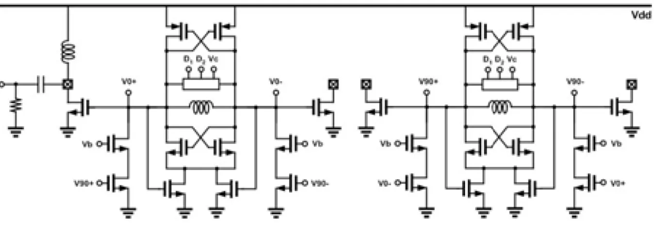
The complete schematic of the quadrature-phase VCO is shown in Fig. 2. The quadrature phase of the output signal is obtained by two mutually coupled VCOs. The active coupling pairs are formed by cascode stages to eliminate phase ambiguity and bidirectional coupling [11] while maintaining sufficient transconductance. No additional tail current sources are used for the active coupling pairs, resulting in further reduction of flicker noise.
In order to eliminate the loading effect and to drive the external 50-Ω from the test instruments, open-drain buffers are added for the quadrature outputs. The bias current of the buffer stage is provided by bias-T during measurement.
3. EXPERIMENTAL RESULTS
The quadrature-phase VCO was implemented in a standard 0.18-μm CMOS technology. In order to minimize the phase error of the quadrature output, a symmetrical layout is used for the design. Figure 3 shows the micrograph of the fabricated circuit with a chip size of 1.09 × 0.91 mm2 including the pad frame.
On-wafer probing was performed to characterize the circuit performance. The output spectrum and phase noise of the VCO were measured by an Agilent E4407B spectrum analyzer. Good agreement was obtained between the simulation and measurement.
The VCO core consumes a dc power of 24 mW from a 2-V supply voltage. By switching the binary-weighted capacitor array with a control voltage tuned from 0 to 1.8 V, the 4 overlapping frequency sub-bands of the VCO are shown in Fig. 4. From the measurement results, the VCO demonstrates a maximum output frequency of 9 GHz with a frequency tuning-rangeof16%.
Themeasuredoutput spectrum
Fig. 2 The schematic switched-bias quadrature phase VCO with buffers
Fig. 3 The die photo of QVCO
Fig. 4 2-bit wide tuning frequency range
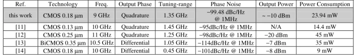
and close-in phase noise at the maximum output frequency of 9 GHz are shown in Figs. 5(a) and 5(b), respectively. The VCO delivered an output power of − 16.51 dB to the 50-Ω test instrument including the losses from the measurement setup, while a phase noise of − 99.48 dBc/Hz is observed at 1-MHz offset frequency. The performance of the quadrature-phase VCO is summarized in Table 1.
(a)
(b)
Fig. 5 (a) The output spectrum of QVCO output. (b) The phase noise of QVCO at 1-MHz frequency offset
Table 1 The performance summary of the QVCO
Ref. Technology Freq. Output Phase Tuning-range Phase Noise Output Power Power Consumption this work CMOS 0.18 μm 9 GHz Quadrature 1.35 GHz −99.48 dBc/Hz @ 1MHz ~ −10 dBm 23.94 mW
[11] CMOS 0.13 μm 10 GHz Quadrature 1.45 GHz −95dBc/Hz @ 1MHz N/A 14.4 mW [12] CMOS 0.25 μm 11 GHz Quadrature 1.25 GHz −98dBc/Hz @ 1MHz −20 dBm 45 mW [13] BiCMOS 0.35 μm 10.5 GHz Differential 1.05 GHz −114dBc/Hz @ 1MHz −7 dBm 35 mW [14] CMOS 0.18 μm 10 GHz Differential 0.45 GHz −101dBc/Hz @ 1MHz −8 dBm 9 mW
4. CONCLUSIONS
A 9-GHz quadreture-phase VCO is presented in this paper. Fabricated in a 0.18-μm CMOS process, the VCO exhibits a maximum output frequency of 9-GHz with a 16% tuning-range. By employing the complementary cross-coupled pairs and switched-bias technique for phase noise reduction, the VCO demonstrates a phase noise of −99.48 dBc/Hz at 1-MHz offset frequency. The VCO core consumes a dc power of 23.94 mW from a supply voltage of 2 V.
ACKNOWLEDGEMENT
This work was supported in part by the National Science Council under Grant No. 93-2220-E-002-003 and 93-2220-E-002-009. The authors would like to thank National Chip Implementation Center (CIC) for chip fabrication and technical supports.
REFERENCES
[1] M. Vanmackelberg, et al., “90 nm SOI-CMOS of 150 GHz fmax and 0.8 dB NFmin @6GHz for SOC,”
IEEE Int. SOI Conference, Oct. 2002, pp.
153−154.
[2] D. Yamazaki, et al., “A 25 GHz clock buffer and a 50 Gb/s 2:1 selector in 90 nm CMOS,” in IEEE Int.
Solid-State Circuits Conf. Dig. Tech. Papers, Vol.
1, Feb. 2004, pp. 240–525.
[3] T. Yamamoto, et al., “A 43 Gb/s 2:1 selector IC in 90 nm CMOS technology,” IEEE Int. Solid-State
Circuits Conf. Dig. Tech. Papers, Vol. 1, Feb.
2004, pp. 238−239.
[4] P. Hazucha, et al., “A 233MHz, 80-87% efficient, integrated, 4-phase DC-DC converter in 90 nm
CMOS,” Symposium on VLSI Circuits Dig. Tech.
Papers, June 2004, pp. 256–257.
[5] W. Jeamsaksiri, et al., “Integration of a 90 nm RF CMOS technology (200 GHz fmax ~ 150GHz fT
NMOS) demonstrated on a 5 GHz LNA,”
Symposium on VLSI Circuits Dig. Tech. Papers,
June 2004, pp. 100–101,
[6] B. Razavi, Design of Integrated Circuits for
Optical Communications, McGraw-Hill, 2003.
[7] A. Hajimiri and T. H. Lee, “Design issues in CMOS differential LC oscillators,” IEEE J.
Solid-State Circuits, Vol. 34, May 1999, pp.
717−724.
[8] E. Hegazi, et al., “A filtering technique to lower LC oscillator phase noise,” IEEE J. Solid-State
Circuits, Vol. 36, Dec. 2001, pp. 1921–1930.
[9] H. Tian and A. E. Gamad, “Analysis of 1/f noise in switched MOSFET circuits,” IEEE Trans. Circuits
and Systems, Vol. 48, Feb. 2001, pp. 151–157.
[10] C. C. Boon, et al., “RF CMOS low-phase-noise LC oscillator through memory reduction tail transistor,” IEEE Trans. Circuits and Systems, Vol. 51, Feb. 2004, pp. 85–90.
[11] L. Shenggao, et al., “A 10-GHz CMOS quadrature LC-VCO for multirate optical applications,” IEEE
J. Solid-State Circuits, Vol. 38, Oct. 2003, pp.
1626–1634.
[12] T. P. Liu, “1.5 V 10-12.5 GHz integrated CMOS oscillators,” Symposium on VLSI Circuits Dig.
Tech. Papers, June 1999, pp. 55−56.
[13] H. Wu and A. Hajimiri, “A 10 GHz CMOS distributed voltage controlled oscillator,” IEEE
CICC, May 2000, pp. 581−584.
[14] A. H. Mostafa and M. N. El-Gamal, “A CMOS VCO architecture suitable for sub-1 volt high- frequency (8.7-10 GHz) RF applications,” Int.
Symposium on Low Power Electronics and Design,
Ying-Chih Hsu (
徐
英
智
) received the B.S. degree from the National Chiao TungUniversity, Hsinchu, Taiwan in 2003. He is currently working toward the M.S. degree in National Taiwan University, Graduate Institute of Electronics Engineering, where he is a member of the Analog Design and System Integration Lab. His research topics are focused on CMOS high-speed multi-phase VCO designs.
Liang-Hung Lu (
呂
良
鴻
) was born in Taipei, Taiwan, R.O.C., in 1968. He received theB.S. and M.S. degrees in electronics engineering from National Chiao-Tung University in 1991 and 1993, respectively. He received the Ph.D. degree in electrical engineering from the University of Michigan, Ann Arbor, in 2001. During his graduate study, he was involved in SiGe HBT technology and monolithic microwave integrated circuit (MMIC) applications. He joined IBM Semiconductor Research and Development Center (SRDC), Hopewell Junction, NY, in 2001, where he was engaged in low-power and RF project for silicon-on-insulator (SOI) technology. In the August of 2002, he joined the faculty of theDepartment of Electrical Engineering in National Taiwan University as an Assistant Professor. His research interests include design and fabrication of MMIC for wireless communication, CMOS/BiCMOS RF and mixed-signal integrated circuit design.
收稿日期94 年 3 月 2 日、接受日期 94 年 4 月 30 日 Manuscript received March 2, 2005, accepted April 30, 2005