國
國
國
國
立
立
立
立
交
交
交
交
通
通
通
通
大
大
大
大
學
學
學
學
加速器光源科技與應用
加速器光源科技與應用
加速器光源科技與應用
加速器光源科技與應用碩士學位學程
碩士學位學程
碩士學位學程
碩士學位學程
碩
碩
碩
碩
士
士
士
士
論
論
論
論
文
文
文
文
極紫外光微影之鉬矽多層膜鏡片與光罩
極紫外光微影之鉬矽多層膜鏡片與光罩
極紫外光微影之鉬矽多層膜鏡片與光罩
極紫外光微影之鉬矽多層膜鏡片與光罩
反射率
反射率
反射率
反射率改善研究
改善研究
改善研究
改善研究
Reflectance Improvement of Mo/Si Multilayer Mirrors
and Masks for Extreme Ultra-Violet Lithography
研 究 生 :劉芳宜 Fang-Yi Liu
指導教授 :黃遠東 教授 Prof. Yang-Tung Huang
許博淵 博士 Dr. Bor-Yuan Shew
極紫外光微影之鉬矽多層膜
極紫外光微影之鉬矽多層膜
極紫外光微影之鉬矽多層膜
極紫外光微影之鉬矽多層膜鏡片與光罩
鏡片與光罩
鏡片與光罩
鏡片與光罩
反射率改善研究
反射率改善研究
反射率改善研究
反射率改善研究
Reflectance Improvement of Mo/Si Multilayer Mirrors
and Masks for Extreme Ultra-Violet Lithography
研 究 生 : 劉芳宜 Student: Fang-Yi Liu
指導教授 : 黃遠東 Advisor: Prof. Yang-Tung Huang
許博淵 Dr. Bor-Yuan Shew
國立交通大學
加速器光源科技與應用碩士學位學程
碩 士 論 文
A Thesis
Submitted to Graduate Program for Science and Technology of
Accelerator Light Source
College of Engineering
National Chiao Tung University
In Partial Fulfillment of the Requirements
For the Degree of Master
In
Graduate Program for Science and Technology of Accelerator Light Source
January 2012
Hsinchu, Taiwan, Republic of China
極紫外光微影之鉬矽多層膜鏡片與光罩
反射率改善研究
研究生: 劉芳宜 指導教授: 黃遠東 教授
許博淵 博士
國立交通大學
加速器光源科技與應用碩士學位學程
摘 要
本研究主要探討極紫外光微影之鉬矽多層結構之設計與特性。其四
分之一波膜反射率可以藉由調整膜層厚度的最佳化程序達到較好效能,
而於商業用的極紫外光微影系統其要求多層膜需具備高反射率效果及較
好的穩定性。本研究以介面工程 (interface-engineered) 完成了在 13.5-nm
波長具有 72.62%反射率及 0.828 nm 半高全寬介面工程鉬矽(Mo/Si)多層膜
結構之開發,此結構則包含被 boron carbide (B
4C) 與 ruthenium (Ru) 材料
所分隔的鉬矽交錯層,Ru 和 B
4C 的屏障層 (barrier layer) 則被分別插入
於 鉬 和 矽 (Mo-on-Si) 及 矽 和 鉬 (Si-on-Mo) 的 介 面 中 形 成 54 對 的
Ru/Mo/B
4C/Si 多層膜。與傳統的四分之一波膜相比,在 13.5-nm 波長大
約有 4%的反射率改善,將 1.4 nm 厚的 Ru 的 0.2 nm 厚的 B
4C 插入鉬矽多
層膜的介面可以達到此最佳反射率。另外,現今主要關注的議題之一是
由於表面光子輻射所導致的光學式表面汙染將會減低光電元件的使用壽
命;而從模擬結果看來最有希望成為覆蓋層 (capping layer) 的材料是 Ru。
藉由將 Ru 覆蓋於介面工程鉬矽多層膜結構最上層可達到對極紫外光的
氧化抵抗力,在經由極紫外光曝光環境的過程中這個結構能夠具有高反
射率以及抗氧化力。
Reflectance Improvement of Mo/Si Multilayer Mirrors and Masks
for Extreme Ultra-Violet Lithography
Student: Fang-Yi Liu Advisor: Prof. Yang-Tung Huang
Dr. Bor-Yuan Shew
Graduate Program for Science and Technology of
Accelerator Light Source
National Chiao Tung University
ABSTRACT
In this study, the design and characteristics of Mo/Si multilayers for extreme ultra-violet (EUV) lithography have been investigated. The reflectance of the quarter-wavelength multilayers can be enhanced further by optimized procedures with which the layer thicknesses are varied for best performance. For commercial EUV lithographic systems multilayer mirrors and masks require with higher reflectance and better stability. Interface-engineered Mo/Si multilayers with 72.62% reflectance and a FWHM of 0.828 nm at 13.5-nm wavelength have been developed and simulated. The design was achieved with 54 pairs of Ru/Mo/B4C/Si multilayer. This structure consist of alternating Mo
and Si layers separated by thin boron carbide (B4C) and ruthenium (Ru) layers. Ru barrier
layer was inserted into a Mo-on-Si interface and B4C barrier layer was inserted into a
Si-on-Mo interface to improve the EUV reflective multilayer properties. About 4 % improvement of the reflectance at 13.5-nm wavelength compared to standard quarter-wave stacks can be acquired by the design. The best results according to simulation were obtained with 1.4-nm-thick Ru layers for the Mo-on-Si interfaces and 0.2-nm-thick B4C layers for the
Si-on-Mo interfaces. The contaminations of optical surfaces by photon irradiation in the presence shorten optics lifetime become one of the main concerns. From simulation results, the most promising candidate seems to be Ru. The improvement in oxidation resistance of EUV multilayers has been achieved with Ru -capped interface-engineered Mo/Si multilayers. This structure achieves high reflectance and the great oxidation resistance during the EUV exposure in a water-vapor (oxidized) environment. Based on simulation results, we calculated reflectance for the reflective multilayer mirrors in a EUVL procedure and concluded that Ru-capped Ru/Mo/B4C/Si multilayers have a higher performance than
quarter-wave Mo/Si multilayers. The simulation results clearly show reflectance improvement of our designed structure compared with standard Mo/Si multilayer structures.
誌謝
漫長的碩士生涯終於要結束了,想想過去兩年多在模擬上經歷了很
多挫折,從不熟悉語言程式的門外漢到現在可以又驕傲又獨立的寫出一
些有意義成果的 code。曾經無助、沮喪的想就此放棄,卻也一路上得到
了很多人鼓勵和協助才能夠撐到這篇論文的誕生,就讓我利用這短短的
篇幅獻上最深切的感謝。
指導教授黃遠東博士以平時對英文的要求督促我以英文完成本篇論
文,且熟悉於人際關係的行為模式令人十分佩服,是我值得學習的典範。
非常謝謝老師在實驗模擬上讓我有很大的空間自己探究、摸索以及之後
次次詳細的論文修改,讓我在這兩年半的時間裡對於人事物有所成長。
接著是對於 EUV 這個領域雖然不太了解,卻也能夠適時以其原本的聰明
才智進而提點我的徐新峰學長,努力不懈的研究精神讓人佩服,祝福你快
點拿到博士學位找到心目中的工作。還要感謝能在碩士生涯遇見的蘇婷
婷、程建瑋、張書維、邱霆宇、楊智翔、許茗舜的你們,感謝在我苦悶
的課業生活上給予幫助及帶來歡笑和感動。還有實驗室的陳建華、劉宇
修、謝宗謀、蘇倉賢和黃一平學長們與林政文、李承翰、蔡翼鍾、廖浚
宏學弟們都很謝謝你們這些日子以來的鼓勵和幫助。
即使山上的風太大了,慢慢走還是會抵達的,一定可以走完最後一
里路;這些日子過得好久好長,卻又在眨眼之間消逝,也許選擇了一條
顛頗的道路,但不管多麼崎嶇還是能遇見終點的。最後的最後,我很愛
也愛著我的家人,感謝你們的溫暖支持總是給予適時心靈幫助,謝謝!!
Contents
Contents iv
List of Tables vi
List of Figures viii
1 Introduction 1
1.1 The Evolution of Lithography . . . 1
1.2 Extreme Ultra-Violet Lithography . . . 3
1.3 Optics of EUVL Systems . . . 5
2 Analytic Theories and Method 8 2.1 Introduction . . . 8
2.2 Transfer Matrix Method . . . 8
2.2.1 TE Mode and TM Mode . . . 10
2.2.2 Re‡ection and Transmission Coe¢ cients . . . 11
3 Multilayer Consideration for EUVL 16 3.1 Introduction . . . 16
3.2 Basic Principle of Multilayers . . . 16
3.3 Choice of Multilayer Materials and Wavelength Considerations . . . 18
3.4 Multilayer Deposition Technologies . . . 23
3.5 Optical Constants . . . 24
3.6 Throughput . . . 25
4.2 Mo/Si Multilayer Structure for EUV Lithography . . . 27
4.2.1 Design Consideration for a Mo/Si Multilayer Structure . . . 27
4.2.2 Re‡ectance Optimization for a Mo/Si Multilayer Structure . . . . 30
4.3 Interface-Engineered Multilayer Structure . . . 35
4.3.1 Design Consideration for an Interface-Engineered Multilayer Struc-ture . . . 35
4.3.2 Re‡ectance Optimization with Di¤erent Barrier Layers in a Mo/Si Multilayer Structure . . . 36
4.4 Capping Layer to Avoid the Oxidation . . . 47
4.4.1 Design Consideration with a Capping Layer . . . 47
4.4.2 Material Selection for the Capping Layer . . . 48
4.4.3 Re‡ectance Optimization for the Interface-Engineered Multilayer Structure with a Capping Layer . . . 51
5 Conclusion 55
List of Tables
3.1 Values of n and k at 13.5 nm. . . 25 4.1 Re‡ectance versus individual thickness of Mo and Si layer. . . 32 4.2 The maximum re‡ectance at 13.5-nm wavelength of …ne-tuned Mo/Si ML
structure with an increasing pair number. . . 33 4.3 Parameters of three kinds of Si-based ML structures. . . 33 4.4 The detailed parameters of interface-engineered B4C/Mo/Si ML structure
at Mo-on-Si interface. . . 41 4.5 The detailed parameters of interface-engineered C/Mo/Si ML structure at
Mo-on-Si interface. . . 41 4.6 The detailed parameters of interface-engineered Ru/Mo/Si ML structure
at Mo-on-Si interface. . . 41 4.7 The detailed parameters of interface-engineered Mo/B4C/Si ML structure
at Si-on-Mo interface. . . 42 4.8 The detailed parameters of interface-engineered Mo/C/Si ML structure at
Si-on-Mo interface. . . 42 4.9 The detailed parameters of interface-engineered Mo/Ru/Si ML structure
at Si-on-Mo interface. . . 42 4.10 The detailed parameters of interface-engineered Ru/Mo/B4C/Si ML
struc-ture. . . 43 4.11 The detailed parameters of interface-engineered Ru/Mo/B4C/Si ML
struc-ture with thickness dependent. . . 44 4.12 The detailed parameters of interface-engineered Ru/Mo/B4C/Si ML
4.13 The detailed parameters of interface-engineered Ru/Mo/B4C/Si ML
struc-ture with thickness dependent. . . 44 4.14 The detailed parameters of interface-engineered Ru/Mo/B4C/Si ML
struc-ture with thickness dependent. . . 44 4.15 The detailed parameters of interface-engineered Ru/Mo/B4C/Si ML
struc-ture with thickness dependent. . . 45 4.16 The detailed parameters of interface-engineered Ru/Mo/Si, Mo/B4C/Si,
and Ru/Mo/B4C/Si ML structures. . . 45
4.17 The detailed parameters of interface-engineered Mo/Si ML structure and Ru/Mo/B4C/Si ML structure. . . 46
4.18 The detailed parameters of Mo/Si ML structure, Ru/Mo/B4C/Si ML
structure, and Ru/Mo/B4C/Si ML structure with a 2.0-nm Ru as a
List of Figures
1-1 Illustration of the imprint lithography process. . . 6 1-2 Schematic of the imprint lithography system. . . 7 1-3 Schematic of the extreme ultra-violet (EUV) lithography system. . . 7 2-1 Sketch of the coordinate system, and the wave axis is chosen to coincide
with the z-axis. . . 10 2-2 Sketch of the m-layer multilayer structure. . . 11 2-3 Sketch of the equivalent admittance of interfaces a and b. . . 12 3-1 Schematic with the intensity I0 of incident x-ray and the intensity It of
being transmitted through by the sample. . . 18 3-2 Schematic progression of the linear absorption coe¢ cient of wavelength. . 20 3-3 The left side is a simpli…ed illustration of Bohr atomic model and the right
side is a comparison of continuum level versus absorption edge overplotted. 21 3-4 Theoretical multilayer survey: Maximum achieveable normal incidence
re-‡ectance in the soft x-ray range for the systems shown. . . 22 3-5 (a) Side view of the LLNL large-optics DC-magnetron sputtering system.
(b) An optic introduced into the chamber through a side door. . . 24 3-6 TEM cross-section of a Mo/Si multilayer is showing crystalline Mo and
amorphous Si. The right image shows the top part of the multilayer, including the capping layer. . . 26 4-1 The simple schematic illustration of an EUVL projection system. . . 29 4-2 The schematic diagram of the Mo/Si multilayer. . . 29 4-3 The spectral response for quarter-wave stack and …ne-tuned Mo/Si ML
4-4 The re‡ectance versus the pair number for the …ne-tuned Mo/Si ML struc-ture. . . 34 4-5 The spectral re‡ectance comparison of the quarter-wave stack, …ne-tuned
Mo/Si ML structure and Mo/Si ML structure. . . 34 4-6 Distribution of the electrical …eld intensity within the Mo/Si multilayer
structure in the case of maximum re‡ectance. The …eld intensity is high at the interfaces Si-on-Mo and low at the Mo-on-Si interfaces. . . 36 4-7 Calculations of EUV re‡ectance depending on the thickness of B4C, C,
and Ru barrier layers at the Mo-on-Si interface. . . 37 4-8 Calculations of EUV re‡ectance depending on the thicknesses of B4C, C,
and Ru barrier layers at the Si-on-Mo interface. . . 38 4-9 Calculations of EUV re‡ectance depending on the thickness of B4C, C,
and Ru barrier layers at the Mo-on-Si interface. . . 39 4-10 Calculations of EUV re‡ectance depending on the thickness of B4C, C,
and Ru barrier layers at the Mo-on-Si interface. . . 39 4-11 Calculations of EUV re‡ectance depending on the thicknesses of B4C, C,
and Ru barrier layers at the Si-on-Mo interface. . . 40 4-12 Calculations of EUV re‡ectance depending on the thicknesses of B4C, C,
and Ru barrier layers at the Si-on-Mo interface. . . 40 4-13 The spectral re‡ectance comparison of the Ru/Mo/Si ML structure, Mo/B4C/Si
ML structure, and Ru/Mo/B4C/Si ML structure. . . 45
4-14 The spectral re‡ectance comparison of the Mo/Si ML structure and Ru/Mo/B4C/Si
ML structure. . . 46 4-15 All non-shaded elements in the periodic table have good optical properties. 49 4-16 The re‡ectance versus the capping thickness with di¤erent kinds of
mate-rials on Ru/Mo/B4C/Si ML structure. . . 52
4-17 The re‡ectance versus the capping thickness with the Ru/Mo/B4C/Si ML
structure and Ru as the capping material. . . 53 4-18 The spectral re‡ectance comparison for Mo/Si ML structure, Ru/Mo/B4C/Si
ML structure, and Ru/Mo/B4C/Si ML structure with a 2.0-nm Ru as a
Chapter 1
Introduction
1.1
The Evolution of Lithography
The fast development in manufacturing technology of integrated circuits has followed the Moore’s law for years; and the number of transistors on a chip has grown doubling on the average of every 18 months exponentially. The role of lithography has been more important not only because of the requirements for smaller feature sizes and tighter overlay, but also because of the increasing costs of lithography tools [1].
The fundamental relationship in lithographic imaging system is resolution which can be described
Resolution = k1 =NA (1.1)
where k1 is constant, is the wavelength of the imaging radiation, and NA is the
numer-ical aperture of the imaging system.
Therefore, when IC feature size shrank, the indusry used the expose source from g-line (436 nm), ultraviolet (365 nm), 248-nm KrF, to 193-nm ArF by excimer lasers in lithography technology [2]. In the 193-nm stage, even the multiple patterns where used to achieve the 22-nm pitch. Regardless of what method, high throughput and low cost of ownership must be satis…ed [3], [4]. The following will list some methods for the next generation lithography (NGL), and several unique challenges also would be introduced.
Figure 1-1 shows the equipment of the imprint lithography. The pattern is created on a template made of glass. Then a template is pressed on the coating resist to transfer the pattern. Exposing with an ultraviolet light, let the photoresist react and form a pattern.
To reduce the linewidth, the 1X mask should be smaller; moreover, defects in the pattern must be below 10% of the width of the feature. And the resist should be with a lower viscosity for su¢ cient throughput. In addition, the production costs include the template life time and imprint material cannot be too high.
Electron beam lithography is a kind of maskless lithography, and Figure 1-2 shows the equipment set-up of e-beam lithography system [5]. Electron beam method is used to create patterns on a wafer directly and a smaller beam source could achieve a smaller line width. Maskless lithography eliminates the problems of mask lifetime and mask defect. Although there is no mask cost in direct-writing lithography, e-beam lithography need overcome the major challenge is the wafer throughput. Multiple-beam direct writing is developed for improving throughput, and the system combining with the resist sensitivity may provide a higher resolution. Besides, another problem in e-beam lithography is the inaccuracies on the wafer due to the charging e¤ect.
One of the earliest and most important decisions made in the …eld of EUVL was the choice of the exposure wavelength. That in‡uenced the design of the projection optics, set the peak re‡ectance and bandwidth of the multilayer re‡ective coatings, and had an impact on the performance of EUV materials. Figure 1-3 shows the equipment set-up of EUV lithography [6]. The wavelength in this region is shorter than other exposure sources in lithography, which wiil be absorbed in most materials, and thus all equipment should be enclosed in a high vacuum environment. Furthermore, to avoid EUV absorption, optics and mask in the system are re‡ective and defect-free by multilayer-coating mirrors, i.e., the quarter-wave Bragg re‡ectors. Then higher image contrast is one of advantages of EUVL, which means that masks will not require the expensive optical proximity correction (OPC) and phase shifting. Although the cost of ownership (CoO) of EUVL is lower than other methods, there are still many problems to be solved such as the source e¢ ciency, the mirror re‡ectance, the incident angle, and the thickness of the multilayer.
1.2
Extreme Ultra-Violet Lithography
At normal incidence, no material provides more than about 1% re‡ectance in the EUV spectral region at wavelengths below 30 nm, because the index of refraction of all ma-terials in this region is approaching unity. The original idea to use soft x-rays in the 4 nm to 40 nm wavelength range is during the 1980s [7] - [10]. In 1972, E. Spiller of IBM showed that multilayer structures composed of thin layers of materials that have widely di¤erent EUV absorption values can lead to constructive interference and there-fore enhanced re‡ectance. In 1985, T. Barbee , S. Mrowka, and M. Hettrick changed the multilayer structure by molybdenum-silicon (Mo/Si) instead of tungsten-carbon (W/C) around 20-nm wavelength. Replacing new material coated on the wafer got a better re‡ectance [11]. In 1988, A. Hawryluk and L. Seppala of Lawrence Livermore National Laboratory (LLNL) invented two-mirror system. In 1989, A. Hawryluk, N. Ceglio, and D. Gaines changed the light source to 13-nm wavelength; besides, they changed the mask and the wafer from the concave spherical shape to the ‡at shape. In 1990, the group at AT&T tried to apply the laser technology to lithography. The second stage of EUVL development is focusing on the lager image …leds and smaller wavefront errors. The team of AT&T published the light source from the soft x-ray projection to the extreme ultra-violet. Today, ASML published the alpha demo tool and lots of companies utilized this machine to fabricate on 45-nm test chip [12].
There are several sources for EUVL, such as synchrotron, discharge-produced plasma (DPP), and laser-produced plasmas (LPP). Synchrotron source does not need frequently replace components, but its high cost and large space requirement are big problems. And another source is LPP produced by very-high-intensity pulsed-laser light and focus onto a material accompanies high temperature to create plasmas then high-energy photons are emitted. LPP use di¤erent injection laser target such as xenon, lithium, and tin [13], and usually use noble gas because it is chemically inert [14], [15]. In addition, using noble gas as the EUV radiation materials can increase the conversion e¢ ciency. Today, tin is a dominant candidate because its high e¢ ciency to EUV light and good re‡ectance in the Mo/Si multilayer. To decrease the cost of ownership for NGL, DPP was developed [16]. In an EUV lithography system, all the lenses are re‡ective and defect free. The surface roughness makes a great impact on the image contrast and throughput. Fortunately, the
with repeated high-Z (Z is the atomic number) and low-Z materials can achieve a high re‡ectance. A pair of multilayer (i.e., Mo/Si) thickness is half the wavelength of the EUV source. If the re‡ectance is lower than 70%, the light intensity will be strongly reduced. In addition, we should reduce the thermal impact on the glass substrate to avoid the deformation. Lenses should not be compressed to avoid getting defects. The EUV source such as plasma with a high EUV intensity will destroy the optics. Fortunately, the laser source is distant from optics that leave the heat to protect from deformation amd extend the life time of optics. On the other hand, because of the EUV source plasma will produce erosion of multilayer, it will get much more erosion. In EUV lithography systems, there are an even number of mirrors. If it is not necessary, there is no need to add optics, because adding mirrors will decrease the transmission rate of light.
EUVL mask is a blank mask to be pattern. The fundamental properties of the blank mask are ‡at, defect-free, and thermal independently. It is important to consider the thermal problem because the mask absorbs EUV energy which results in the thermal expansion. The tolerance of critical defect dimension is according to 80% half-pitch technology node. Now the defect in the multilayer can be removed by focused ion beam (FIB) [17]. For the mask applications, above the Mo/Si multilayer are the absorber layer and the anti-re‡ective coating layer to form the low-re‡ectance region. Ta-based materials are good candidate as absorber layer such as TaBN, TaN and TaSi in EUVL [18], [19]. SiON, Si3N4 and Al2O3 are used as the anti-re‡ective coating layer [20], [21].
When the critical dimension (CD) shrink, the line edge roughness (LER) does not decrease with expected. The CD resolution and line LER are big challenges for the NGL [22], [23]. Chemically ampli…ed resist (CAR) is used for 193 nm and 248 nm optical lithography. However, CAR absorbs EUV light which cause the LER and the pattern collapsed. Thus, poly methyl methacrylate (PMMA) is a better option for an EVL system. In addition, the pattern collapse depends on the aspect ratio, so we expect that the aspect ratio will be lager than 3 in usual, but it only achieve 2 or less in practice. Besides, there are still many challenges such as sensitivity, resolution, out-gassing and so on. Among these challenges, out-gassing not only pollutes the optics but also shrinks the lifetime of optics. Even a higher sensitivity resist would generate more byproducts as well. Recently, resist must be needed to continue to develope.
1.3
Optics of EUVL Systems
Compared to optical systems that operate at visible or near-visible wavelengths, EUVL error budgets translate into very tight …gure speci…cations for the mirror substrates and coatings that comprise the EUVL system. The mirror surface roughness in the mid and high spatial frequency ranges is also a crucial property because it a¤ects the imaging contrast and throughput of the lithography system. As a result, the pattern and coat-ings in a production-scale EUVL system must be controlled to the order of subatomic dimensions. During the past few decades, the requirements imposed on the system wave-front error, on the mirror …gure, and on the re‡ective properties and thickness control of EUV multilayer thin …lms have led to enormous advancements in optical manufactur-ing and multilayer coatmanufactur-ing technology. Scienti…c areas such as solar physics, astronomy, x-ray microscopy, and plasma diagnostics that need similar instrumentation technology have greatly bene…ted by the improvements in EUV/x-ray optics. The EUV wavelength of illumination determinates the use of re‡ective optical elements as opposed to the re-fractive lenses used in conventional lithographic systems. Thus, EUVL tools are based on all-re‡ective concepts: multilayer (ML) coated optics for the illumination and pro-jection systems, and a ML-coated re‡ective mask. To achieve the production-quality lithographic imaging, EUVL systems must be very well-corrected for aberrations. In EUVL, the re‡ective multilayers are used for applications as masks and as well as mir-rors in exposure systems. Examples of high re‡ectance EUV mirmir-rors for near-normal incidence operation are Mo/Be and Mo/Si multilayer that exhibit high re‡ectance in the 11.2-12.0 nm and 12.8-14.0 nm spectral regions, respectively [24] - [26]. The motivation behind this work is the need for optical throughput enhancement which is based on the re‡ectance improvement of multilayer structures in an EUV projection lithographic sys-tem. Furthermore, the ML coatings with normal-incidence experimental re‡ectance of 70% have been demonstrated in the 11 nm to 14 nm wavelength range.
In this study, we have designed a highly re‡ective multilayer with interface-engineered structure, and we also have investigated their characteristics. Here, we organize an out-line of the thesis as follows. In Chapters 2, the numercial method with the transfer matrix to perform the analysis of the multilayer structures will be discussed the re‡ectance for the multilayer structures could be calculated from the charateristic matrix. In Chapters
viewed. In Chapter 4, kinds of multilayer structures for EUV lithography system will be discussed, and the simulation results will be given. It can be seen that the thin-…lm optimization techniques are essential for achieving re‡ectance improvements for the EUV multilayer structures. The optimization procedures employed in this thesis are an inte-gral part of the Matlab software. The notation we have adopted to represent a period in a multicomponent stack is based on the commonly-used two-component stack at 13.5-nm wavelength, e.g. Mo/Si, where Mo is the low and Si is the high refractive index material. In Chapter 5, conclusion will be given and future work will be suggested.
Figure 1-2: Schematic of the imprint lithography system.
Chapter 2
Analytic Theories and Method
2.1
Introduction
In this chapter, we will review the method of analyzing wave propagation in an optical thin …lm. The transfer matrix method [28] is used to perform the analysis of multilayer structures. In order to analyze electromagnetic …eld in optical thin …lms, the polarized electromagnetic plane waves is applied. Finally, the transmittance and re‡ectance for the multilayer can be calculated from the charateristic matrix and observed the wave propagation behavior.
2.2
Transfer Matrix Method
The mathematical physical principles to rule the electromagnetic problems are the Maxwell’s equations. For uniform dielectric and non-uniform dielectric, the Maxwell’s equations (governing the electromagnetic …elds) can be expressed in the following form :
5 E = @B @t, (2.1) 5 H = J +@D @t , (2.2) 5 D = , (2.3) 5 B = 0, (2.4) J = E ; D = E ; B = H, (2.5)
where is the charge density, is the electrical conductivity, is the permittivity, and is the magnetic permeability. By solving the above equation, we can get the plane wave equation as follow:
5 D = 5 ( E) = 5 E + E 5 = 0,
) 5 E = E r = E r (ln ) ,
and from equation 5 5 E = 5(5 E) 52E, we can get
5 @t@ H =5 [ E r (ln )] r2E, ) @ @t[ r H + (r ) H] = r [ E r (ln )] r 2 E, ) @E @t + @2E @t2 + (r ) @H @t =r [ E r (ln )] r 2E, ) r2 E +r [E r (ln )] = @E @t + @2E @t2 r ( 5 E),
and assume the solution of this equation is E = E (x; y; z) ei!t, then the above equation
could be derived as r2E +r [E r (ln )] = i ! !2 E r (ln ) (5 E) = c!2E r (ln ) (r E), where c = i !. (2.6)
We can get the equation of the electric …eld as
r2E + !2 cE +r [E r (ln )] + r (ln ) (r E) = 0, (2.7)
and the equation of the magnetic …eld as
and Eqs. (2.7) and (2.8) can be simpli…ed as,
r2E + !2 cE +r Ez
@ ln
@z = 0, (2.9)
r2H + !2 cH +r (ln c) (r H) = 0. (2.10)
Figure 2-1 shows a coordinate system,which indicates the light is alone the z-direction. Relative to this geometry, we distinguished the transverse electric (TE) mode that the electric …eld is perpendicular to the direction of propagation and transverse magnetic (TM) mode that the magnetic …eld is perpendicular to the direction of propagation. In the following, we derive the wave equation governing the two mode types.
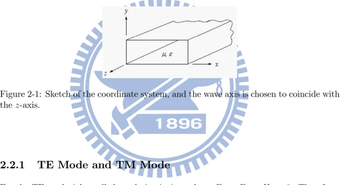
Figure 2-1: Sketch of the coordinate system, and the wave axis is chosen to coincide with the z-axis.
2.2.1
TE Mode and TM Mode
For the TE mode (also called s-polarization), we have Ex = Ez = Hy = 0. Then from
Eqs. (2.9) and (2.10), we obtain the relations : @2 @x2 + @2 @z2 Ey+ ! 2 cEy = 0, (2.11) @2 @x2 + @2 @z2 Hx+ ! 2 cHx+ @ @z ln @ @xHz @ @zHx = 0, (2.12) @2 @x2 + @2 @z2 Hz+ ! 2 cHz = 0. (2.13)
For the TM mode (also called p-polarization), we have Hx = Hz = Ey = 0. Similarly to
Eqs. (2.9) and (2.10), we obtain the relations : @2 @x2 + @2 @z2 Hy + ! 2 cHy @ @z ln c @Hy @z = 0, (2.14) @2 @x2 + @2 @z2 Ex+ ! 2 cEx+ @ @xEz @ @z ln = 0, (2.15) @2 @x2 + @2 @z2 Ez+ ! 2 cEz+ @ @zEz @ @z ln + Ez @2 @z2 ln = 0, (2.16)
2.2.2
Re‡ection and Transmission Coe¢ cients
For a stack of thin, plane, parallel …lms of materials covering the surface of a substrate as shown in Figure 2-2, the refractive indexs are Nj and the layer thicknesses are dj, where
j = 1to m. For discussing easily, we assume that there is only a single thin …lm layer of index N between the substrate (interface b) and incident medium (interface a), the whole dielectric is uniform and isotropy and the surface is parallel and in…nite extensibility as shown in Figure 2-3 [27]. To the form of the plane wave can be described as
ei[!t 2 N z] / e i2 N z = e i , where the phase di¤erence is = 2 N d.
Figure 2-3: Sketch of the equivalent admittance of interfaces a and b.
For the normal incidence, the electromagnetic …elds E and H are continuous at the interfaces, and we can get the relations as follows :
interface b : Eb = Esb+ = E + 1b+ E1b, (2.17) Hb = Hsb+= H1b++ H1b, or sEb = sE + sb = E + 1b E1b, (2.18) interface a : Ea = E0a+ + E0a = E + 1a+ E1a, (2.19) Ha = H0a+ + H0a = H + 1a+ H1a = 0E + 0a 0E0a = E + 1a E1a, (2.20)
where 0, , and s are the optical admittance of incident medium, thin …lms and sub-strate, respectively. There is a phase di¤erence between surfaces a and b when the
electric …elds across the thin …lm. So we have the relation
E1a+ = E1b+ei , (2.21)
E1a = E1be i . (2.22) From Eqs. (2.17) and (2.18), we can get
E1b+ = Eb+ Hb
2 and E1b=
Eb Hb
then Ea = E1a+ + E1a= E + 1be i + E 1be i = Eb+ Hb 2 e i + Eb Hb 2 e i = Ebcos + Hb i sin , (2.23) Ha = H1a+ + H1a = E + 1be i E 1be i = Eb+ Hb 2 e i Eb Hb 2 e i = Eb(i sin ) + Hbcos . (2.24)
Eqs. (2.23) and (2.24) can be written as vector form M as 2 4 Ea Ha 3 5 = 2 4 cos i sin i sin cos 3 5 2 4 Eb Hb 3 5 , (2.25)
and the characteristic matrix of the single …lm is
M = 2 4 cos i sin i sin cos 3 5 . (2.26)
Then from Eqs. (2.19) and (2.20), we have the relations
E0a+ = Ea+ Ha
2 0 and E0a =
0Ea Ha
2 0 .
Once the charateristic matrix of a multilayer stack is known, one can easily determine the re‡ection and transmission coe¢ cients for light incident on the stack. Hence, the re‡ection and transmission coe¢ cients are derived as follows, respectively.
= E0a E0a+ = 0Ea Ha 0Ea+ Ha = 0 Y 0+ Y , (2.27) E 2 E 2 Eb
Both sides of Eq. (2.25) are divided by Eb, where Yb = HEb
b which is equal to the admittance
of the substrate (Ys); then rewriting Eq. (2.25), we can obtain
2 4 B C 3 5 = 2 4 cos i sin i sin cos 3 5 2 4 1 Ys 3 5 , (2.29)
where the equivalent admittance Y is CB. Then we have
= 0B C
0B + C
, and = 2 0
0B + C
.
Therefore, we have the re‡ectance and the transmittance from the above equations as :
R =j j2 = 0B C 0B + C 0B C 0B + C , (2.30) T = Re(Ys) Y0 j j 2 = 4 0Re(Ys) ( 0B + C) ( 0B + C) . (2.31) Matrix calculations determine the transmittance and re‡ectance pro…le for multilayer structures on a substrate. Consider a loss free multilayer design, normally incident radia-tions, and assume that …lms are optically homogenous. The electric …eld vector (Em) and
the magnetic …eld vector (Hm) at the incident boundary of a …lm at the boundary by the
product of the following matrices per layer. The matrix is calculated at each boundary throughout the multilayer as the magnitude of electric and magnetic …eld vectors alter with the properties of the layer [28]. Application of the appropriate boundary conditions between each layer requires that the tangential components of E and H vectors are con-tinuous across each boundary to the equations of wave propagation. The …elds at other interfaces m 1 are similar to Eqs. (2.23) and (2.24) at the same instant of time and a position with identical x and y coordinates.
And we can obtain the matrix form between the (m 1)-th layer and m th layer as 2 4 Em 1 Hm 1 3 5 = 2 4 cos m i msin m i msin m cos m 3 5 2 4 Em Hm 3 5 .
Solving the above given expressions, the matrix expression for single layer is : M = 2 4 E iF iG H 3 5 ,
where: cos m = E = H, isin m= m = F, i msin m= G.
For a multilayer containing m layers, we have 2 4 E0 H0 3 5 = M1M2M3 Mm 2 4 Em Hm 3 5 = M 2 4 Em Hm 3 5 , where M = m j=1Mj = m j=1 2 4 cos j i j sin j i jsin j cos j 3 5 . (2.32) From Eq. (2.29), 2 4 B C 3
5 is known as the charateristic matrix of the assembly. Then the transmittance and re‡ectance for the multilayer can be calculated from this product matrix by : R = 0B C 0B + C 0B C 0B + C , (2.33) T = 2 0Re(Ys) (BC + B C) ( 0B + C) ( 0B + C) 2 (BC + B C) = 4 0Re(Ys) ( 0B + C) ( 0B + C) . (2.34)
Su¢ cient information is included in Eqs. (2.33) and (2.34) to allow the re‡ectance and transmittance of a thin-…lm assembly to be calculated. The re‡ectance, transmittance, and absorptance are then related by R + T + A = 1. The solution of this matrix theory is for multilayer coatings. However, insight into the properties of thin-…lm assembles cannot easily be gained simply by feeding the calculations into a computer program, and insight is necessary if multilayers are to be designed and if their limitations in use are to be fully understood. An approximate method has also been found useful. Based on the matrix theory, in this thesis we have developed a program by MATLAB 7.1 to design and simulate the performance of multilayer coatings.
Chapter 3
Multilayer Consideration for EUVL
3.1
Introduction
EUV lithography (EUVL) employs illumination wavelengths around 13.5 nm, and in many aspects it is considered an extension of optical lithography, which is used for the high-volume manufacturing (HVM) of today’s microprocessors. The EUV wavelength of illumination dictates the use of re‡ective optical elements (mirrors) as opposed to the refractive lenses used in conventional lithographic systems. Thus, EUVL tools are based on all-re‡ective concepts : multilayer (ML) coated optics for the illumination and projection systems, and a ML-coated re‡ective mask.
3.2
Basic Principle of Multilayers
The basic principle behind the optical design in multilayer mirror is simple. A multilayer is an arti…cial structure with a large number of interfaces. A single interface re‡ects a small fraction of an incident beam; however, the re‡ectance increases dramatically if the re‡ected beams from all the interfaces in the multilayer add in phase. The predomi-nant designs are composed of distributed Bragg condition resembling quarter wavelength stacks with constant …lm thicknesses. These re‡ectance values whilet adequate for optical systems with a few re‡ectors will dramatically diminish the output optical intensity to 6-10% directly before the …rst mirror in a nine-mirror EUV lithographic system. There-fore, it is evident that even an increase of 1-2% in the peak re‡ectance of a single mirror will yield a signi…cant light throughput enhancement in the overall optical system. A
particular problem in the EUV region is that all useful materials absorb the radiation to a certain extent. To reduce the e¤ect on the re‡ectance response of the absorption losses, the thicknesses of the two components of the stack are adjusted to deviate slightly from the optical path length of =4. The highest re‡ectance is usually achieved by choosing materials with the largest di¤erence in refractive indices and extinction coe¢ cients. This means that one material is more absorbing (as spacer layer) while the other material is more transparent (as absorber layer) . For the EUV range, the best material pair seems to be Mo and Si. The thickness of the high absorption layer dh is set slightly lower
than that of the low absorption layer dl, thus the partition ratio = dh=(dh+ dl) of the
multilayer is de…ned. Vinogradov and Zeldovich [29] have calculated as a function of absorption - a value of = 0:4 is commonly used. Also, it is well known for general thin-…lm mirror designs with absorbing …lms and for EUV designs, that a gradual varia-tion of the partivaria-tion ratio through the stack with = 0:3 0:4 at the surface to = 0:5 near the substrate can increase the peak re‡ectance. Such optimized stacks would yield signi…cant throughput enhancements in a nine-mirror optical system.
Up to date, there are several ways to increase the re‡ectance for Mo/Si multilayer which is the most common re‡ectors in soft x-ray range :
(1) Add some extra materials into the prime stack.
(2) One material with better optical constants (i.e. less absorption/small k) is sub-stituted for a material on the fundamental stack.
(3) Using some optimized algorithms to calculate the optimum partition ratio of each pair, and its thickness of each pair in the multilayer.
(4) Using a capping layer which is inactivate to the thin …lm layer can avoid the surface oxidation that led to the reduction of re‡ectance in multilayers.
Once Spiller [24] showed that quarter-wave stacks of absorbing materials can be used e¤ectively as optics in the EUV and soft x-ray regions. In the approximation, the highest re‡ectance is achieved with a material pair that has a minimum absorption and a max-imum di¤erence in the refractive indices among the constituent materials. The theory of quasi-quarter-wave MLs predicts enhanced EUV re‡ectance at 13.5 nm based on the use of thin …lms of several materials with the largest possible refractive index di¤erences. However, such MLs have often performed better only in theory. Other factors, such as the
also play the important roles in the ML …lm performance. The enhanced re‡ectance was demonstrated and studied in MLs with di¤usion barrier layers, whose primary function was to suppress interdi¤usion. Re‡ectance can also be optimized by varying the layer thickness ratio of the individual materials. If MLs must be thermal or radiation stable, the design requires the use of refractive materials such as oxides, carbides, silicides, and alloys, or the introduction of barrier layers that are deposited on interfaces to reduce the interdi¤usion due to elevated temperatures. High-resolution MLs can be achieved by selecting materials with a certain ratio of optical constants, by optimization of layer thickness and of the number of bilayers, and by using higher-re‡ectance orders from ML structures. A wide spectral bandwidth requires a periodic ML design.
3.3
Choice of Multilayer Materials and Wavelength
Considerations
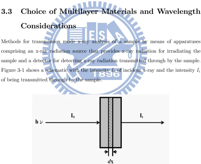
Methods for transmission mode x-ray analysis of a sample by means of apparatuses comprising an x-ray radiation source that provides x-ray radiation for irradiating the sample and a detector for detecting x-ray radiation transmitted through by the sample. Figure 3-1 shows a schematic with the intensity I0 of incident x-ray and the intensity It
of being transmitted through by the sample.
Figure 3-1: Schematic with the intensity I0 of incident x-ray and the intensity It of being
A narrow parallel monochromatic x-ray beam of intensity I0passing through a sample
of thickness dx will get a reduced intensity It according to the expression :
dIt= I0(x) n dx, (3.1)
where dIt is the change in intensity, I0 is the initial intensity, n is the number of
atoms/cm3, is a proportionality constant that re‡ects the total probability of a photon
being scattered or absorbed and dx is the incremental thickness of material transversed. When this equation is integrated, it becomes :
It = I0exp( n x), (3.2)
The number of atoms/cm3 (n) and the proportionality constant ( ) are usually combined
to yield the linear attenuation coe¢ cient ( ). Therefore the equation becomes :
It = I0exp( x). (3.3)
where It is the intensity of photons transmitted across some distance x, I0 is the initial
intensity of photons, is the linear attenuation coe¢ cient, and x is distance traveled. The linear attenuation coe¢ cient ( ) describes the fraction of a beam of x-rays or gamma rays that is absorbed or scattered per unit thickness of the absorber. This value basically accounts for the number of atoms in a cubic cm volume of material and the probability of a photon being scattered or absorbed from the nucleus or an electron of one of these atoms. Using the transmitted intensity equation above, linear attenuation coe¢ cients can be used to make a number of calculations. These include :
(1) the intensity of the energy transmitted through a material when the incident x-ray intensity, the material and the material thickness are known.
(2) the intensity of the incident x-ray energy when the transmitted x-ray intensity, material, and material thickness are known.
(3) the thickness of the material when the incident and transmitted intensity, and the material are known.
trans-Figure 3-2 is an illustration of linear attenuation coe¢ cient ( ) versus wavelength ( ) and we can …nd that is as a function of for every material; however, the extinction coe¢ cient k (the imaginary part of refractive index) is proportional to the linear atten-uation coe¢ cient in accordance with Eq. (3.5). The refractive index is complex, the extinction coe¢ cient introduces a decrease of the amplitude of the waves passing through the material and phase changes between the incident and successively re‡ected waves.
N = 1 i = n ik,
where 1 (n) is the real part of refractive index and (k) is the imaginary part of refractive index. And more speci…cally de…nitions are
= re 2 2 Naf 0 2 and = re 2 2 Naf 0 2 4 , (3.4) = re 2 Amu f10, (3.5)
where re is classical electron radius, Na is the Avogadro’s number, mu is the atomic mass
unit, and f0
1 and f20 are the anomalous dispersion correction factors. And the detail datas
above see Appendix.
Hence, we regard the …gure as a relation chart of extinction coe¢ cient and wavelength underlying the x-ray spectrum. At certain energies where the absorption increases dras-tically, and gives rise to an absorption edge. Each such edge occurs when the energy of the incident photons is just su¢ cient to cause excitation of a core electron of the absorb-ing atom to a continuum state, i.e. to produce a photoelectron. Thus, the energies of the absorbed radiation at these edges correspond to the binding energies of electrons in the K, L, M, etc, shells of the absorbing elements. See Figure 3-3, the absorption edges are labelled in the order of increasing energy, K, LI, LII, LIII, MI, . . . , corresponding
to the excitation of an electron from the 1s (2s
1 / 2), 2s ( 2s 1 / 2), 2p ( 2p 1 / 2), 2p ( 2p 3 / 2), 3s (2s
1 / 2), . . . orbitals (states), respectively. In other words, the absorption e¤ect of
mate-rials would apparently lower and its the key to choose what kind of re‡ector would be in each spetrum.
Figure 3-3: The left side is a simpli…ed illustration of Bohr atomic model and the right side is a comparison of continuum level versus absorption edge overplotted.
We called a light element as spacer (i.e. silicon) that absorbs light only weakly, and a heavy element as absober (i.e. molybdenum) that absorbs light very strongly. However, the reason should be considered is not only the extinction coe¢ cient but easily form an stable and/or sharp interface with other element. At present, the materials of silicon (Si),
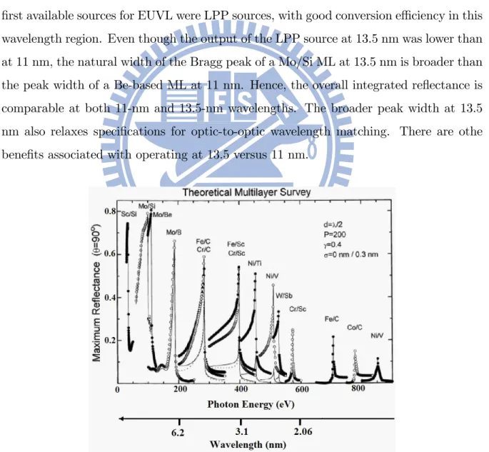
combination of spacer layer is called absorber layer, as well as the extinction coe¢ cient is much larger than spacer layer. To choose those materials have large di¤erence of extinction coe¢ cient but small one is to avoid the incident light would be absorbed completely, thus the re‡ectanec can not be improved. Figure 3-4 [30] is all di¤erent types of general x-ray re‡ectors with its suitable energy (wavelength). The illumination wavelength of 13.5 nm was chosen for EUV lithography based on the early development and good performance of molybdenum-silicon MLs in this wavelength region. Mo/Si still remains the most extensively investigated and best understood ML material pair to date, and 13.5 nm is in the wavelength region just longer than the L2, 3 absorption edge
of Si (12.4 nm), where Mo/Si achieves its best re‡ective performance. In addition, the …rst available sources for EUVL were LPP sources, with good conversion e¢ ciency in this wavelength region. Even though the output of the LPP source at 13.5 nm was lower than at 11 nm, the natural width of the Bragg peak of a Mo/Si ML at 13.5 nm is broader than the peak width of a Be-based ML at 11 nm. Hence, the overall integrated re‡ectance is comparable at both 11-nm and 13.5-nm wavelengths. The broader peak width at 13.5 nm also relaxes speci…cations for optic-to-optic wavelength matching. There are othe bene…ts associated with operating at 13.5 versus 11 nm.
Figure 3-4: Theoretical multilayer survey: Maximum achieveable normal incidence re-‡ectance in the soft x-ray range for the systems shown.
3.4
Multilayer Deposition Technologies
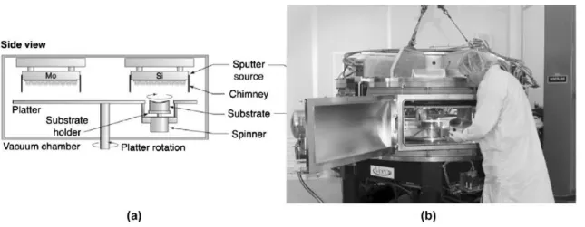
It is well known that the re‡ectance of ML mirrors does not depend only on the materials being used but also on the structural quality of the coatings. Coating quality depends on the deposition method (magnetron-beam sputtering, ion-beam sputtering, electron-beam evaporation, pulsed laser deposition) and the overall deposition control. The …rst ML structures were made by physical vapor deposition (PVD). A nice overview of PVD methods, including thermal and sputter vapor depositions, can be found in Barbee’s review paper. Another way to deposit thin …lms and ML coatings is chemical vapor deposition (CVD), although this technique involves complex chemistry and chemical reactions, often requires a high deposition temperature, and traditionally does not been used to produce EUV MLs. The most commonly used deposition technique for EUVL mirrors is magnetron sputtering. High-quality Mo/Si MLs were already achieved in the mid-1980s. The advantages of this technique are the ability to coat large optics, great control, the stability of the sources, reproducibility from run to run, and a relatively fast sputtering rate. The …rst EUVL optics sets for 0.1-NA full-…eld systems and 0.3-NA micro…eld systems were fabricated using magnetron deposition. An example of a DC-magnetron sputtering system optimized for the coating of large area optics is shown in Figure 3-5 [31]. Similar mirrors for an EUVL process development tool were coated using e-beam evaporation in combination with ion-beam smoothing. High-quality EUV ML coatings are also obtained with ion-beam deposition and ion-assisted deposition. This technique is primarily used to coat EUVL mask blanks because it is a low-defect process. Because of the high energy of impacting ions, this technique also enhances smoothing by increasing the motion of the atoms on the surface. With additional ion polishing, such a technique can relax the requirement for the surface …nish of EUV optics and mask substrates. Another technique is pulsed laser deposition (PLD). Other modes of …lm deposition— though not yet demonstrated— may be possible (e.g., atomic layer deposition (ALD), molecular beam epitaxy (MBE), and modi…ed chemical vapor deposition (CVD) arrangements).
Figure 3-5: (a) Side view of the LLNL large-optics DC-magnetron sputtering system. (b) An optic introduced into the chamber through a side door.
3.5
Optical Constants
To successfully model and predict the performance of ML coatings for EUVL, precise knowledge of the optical properties of a system’s constituent materials is required. The absorptive and dispersive behavior of each material can be obtained from the real and imaginary part of the wavelength-dependent refractive index, also known as optical con-stants. In the EUV/x-ray region, where the wavelength of radiation is comparable to the binding energies of the inner electrons in the material, measurements of the refractive index can be particularly challenging due to sensitivity to surface oxides, contamination, and roughness of the material samples under study. Although sophisticated models have been developed to determine the refractive index of materials using …rst-principles cal-culations, experimental measurements are always recommended as the best method to accurately determine the refractive index of vapor-deposited thin …lms. This is especially true for energy regions in the electronic absorption edges, where the optical properties can strongly depend on experimental conditions such as the method and environment of deposition. The optical constants of important EUVL materials for ML coatings such as Si [32], Mo [33], [34] and Ru [35] have been updated in recent years with more accu-rate experimental results. A comprehensive compilation of the optical constants for all elements in the periodic table, including recently obtained data, are maintained in the Center for X-Ray Optics (CXRO) database [36]. Other databases for the optical prop-erties of materials in the EUV/x-ray region are maintained by the National Institute of
Standards and Technology (NIST) [37] and LLNL [38]. The values of n, k at the EUV wavelengths of particular interesting materials are tabulated in Table 3.1.
Table 3.1: Values of n and k at 13.5 nm.
13.5 nm n k Mo 0.9239 0.0064 Si 0.9999 0.0018 B4C 0.9638 0.0051 C 0.9616 0.0069 Ru 0.8863 0.0171 Pt 0.8907 0.0601 SiO2 0.9781 0.0108 Rh 0.8751 0.0312
3.6
Throughput
An EUVL scanner consists of an all-re‡ective optical system with ML coatings on the projection (imaging) elements, on the condenser/illuminator assembly, and on the mask. All of these elements should be tuned to re‡ect at or near the same wavelength to obtain a substantial output from the system. Any spectral mismatch between the mirrors would translate to throughput reduction. If a goal is set to match the re‡ectance peak position of all EUVL optics to within = 0:05 nm, then in a system with six re‡ections, for example, this level of wavelength matching would ensure at least 97.4% of the ideal throughput. Meeting this goal requires atomic-level repeatability of the coating process from one deposition run to another. In addition to optic-to-optic wavelength matching, another throughput constraint is the tolerance on wavelength variation across the surface of any individual optic in the system. For maximum throughput, the ML should have its re‡ectance peak at the same wavelength for all surface points on any given mirror. If an arbitrary goal is set to stay within 99% of the re‡ectance peak for all points on the optic surface, then a Mo/Si ML operating at = 13.5 nm is allowed to have its wavelength vary to within = 0:05 nm, which is equivalent to having the wavelength (or the thickness) vary from its prescribed value to within 0:37% peak-to-valley (P-V) across the surface.
multilayer-(water vapor and hydrocarbons primarily), which lead to optics contamination (oxidation and carbon deposition). At EUV wavelengths, even a small increase in oxide or carbon layer of only few nanometers could cause a measurable re‡ectance decrease. Nonetheless, re‡ectance has to be stable within 1% in high volume manufacturing (HVM) lithography because the optical throughput is proportional to :
Z m
j=1R
j( )d , (3.6)
where R is the re‡ectance of the m th multilayer mirror and j is the number of re‡ective mirrors in the EUVL tool (Figure 1-3).
These HVM tools might contain 7 or more re‡ective mirrors, and any small change in re‡ectance will lead to a noticeable change in the throughput. Hence, optics lifetime is one of the critical issues for the success of this technology and di¤erent strategies to obstruct oxidation and contamination have been studied [39] - [41]. To extend the lifetimes of the projection optics is by coating the multilayers with thin 2 3-nm capping layer [42] - [44] …lms (Figure 3-6) that reduce the buildup of contamination. In this thesis, we evaluate the solid phase elements in the periodic table and their material combinations as possible capping layer candidates for EUVL applications.
Figure 3-6: TEM cross-section of a Mo/Si multilayer is showing crystalline Mo and amorphous Si. The right image shows the top part of the multilayer, including the capping layer.
Chapter 4
Multilayer Design for High
Re‡ectance in EUV Lithography
4.1
Introduction
Over the past few decades, several lithography techniques have been investigated as sub-stitutes for conventional optical lithography. Among these next generation lithography techniques (NGL), extreme ultraviolet lithography (EUVL) has been considered as one of the most competitive technology owing to its high throughput, similarities with conven-tional optical lithography, and robust mask structure. In EUVL, the re‡ective multilayer structures are used for applications as masks as well as mirrors in exposure systems. Re‡ectance of these multilayers, which is a critical factor for throughput of the EUVL, depends on the structure factors as well as on the material properties.
4.2
Mo/Si Multilayer Structure for EUV
Lithogra-phy
4.2.1
Design Consideration for a Mo/Si Multilayer Structure
At present, there is a considerable interest in mirrors with high re‡ectance at near-normal incidence tuned for the extreme-ultraviolet (EUV) spectral region, most particularly in the 11 14 nm range. This interest is driven by the potential of EUV projection
lithog-tools for fabricating structures below 70 nm. The design of thin-…lm multilayer re‡ectors for the EUV spectral region has been extensively studied by Spiller [24]. Of particular importance for EUV projection lithographic applications are the two-component Mo/Be and Mo/Si multilayer systems that exhibit particularly high theoretical re‡ectance in the 11:3 11:6 nm and 13:0 13:6 nm spectral regions, respectively. The re‡ector designs are composed of distributed Bragg re‡ectors resembling quarter-wavelength stacks with constant …lm thicknesses throughout. The typical designs that have been fabricated are 80 periods of Mo/Be and 40–50 periods of Mo/Si. These designs yield maximum theo-retical re‡ectance of R 78% for the Mo/Be stack and R 74% for the Mo/Si stack. These re‡ectance values which are among the best for multilayer re‡ectors in the EUV region, although adequate for optical systems with a few re‡ectors, will dramatically diminish the output optical intensity to 6–10% of that directly before the …rst mirror. The signi…cance of nine near-normal incidence mirrors is that the number envisaged for an EUV lithography system: two in the illumination optics, six in the imaging optics plus the re‡ecting reticle. It is evident that even a small increase of 1–2% in the peak re‡ectance of a single mirror will yield a signi…cant light throughput enhancement in the optical system.
For Bragg re‡ectors with non-absorbing …lms the optimum optical path di¤erence within each …lm would be a quarter-wavelength. However, a particular problem in the EUV region is that all useful materials absorb the radiation to a certain degree. To reduce the e¤ect on the re‡ectance response of the absorption losses, the thicknesses of the two components of the stack are adjusted slightly from the optical path length of a quarter wavelength. The thickness of the high-absorption layer dh (commonly called the
absorber layer) is set slightly lower than that of the low absorption layer dl (commonly
called the spacer layer); thus the partition ratio = dh=(dh + dl) of the multilayer is
de…ned. A typical multilayer consists of 40 60repeats of this period and usually ends with a Si layer, which partially oxidizes when exposed to air. Mo and Si layers usually act as the absorber layer and the spacer layer, respectively. And the thickness of Mo is designed thinner than that of Si due to the stronger absorption in EUV range. It reveals that the re‡ectance of the EUV multilayer mirror depends on the accurate thicknesses of the stacked layers. The thicknesses of the stacked layers through optimized design can provide the highest re‡ectance for a given wavelength. The pairs of materials, the periodic
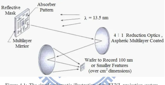
thickness of the multilayer, the thickness ratio, and even the interface roughness are the factors that should be taken into consideration for an optimized design. Figure 4-1 is a illustraion of re‡ective multilayers used for applications as masks and as well as mirrors in exposure systems and Figure 4-2 shows a schematic diagram of the Mo/Si EUV re‡ective multilayer structure. The thickness ratio has a most signi…cant meaning in making a multilayer mirror due to its position of the peak wavelength is mainly determined. In a real lithographic system, which consists of several mirrors, the matching of the thickness ratio in each mirror in accordance with the position of the peak wavelength and the intensity distribution of the re‡ected light is critical for re‡ectance and throughput.
Figure 4-1: The simple schematic illustration of an EUVL projection system.
4.2.2
Re‡ectance Optimization for a Mo/Si Multilayer
Struc-ture
The simulation results in this thesis were all performed by using the language of technical computing design program MATLAB 7.1 (The MathWorks, Inc.), which is based on the characteristic matrix methodology [27] as discussed in Chapter 2. The characteristic matrix of the j th layer of the stack is given by :
Mj = 2 4 cos j i j sin j i jsin j cos j 3 5 , j = 1; 2; 3 ; m where j = 2 Njdj j ,
is the phase thickness expressed in terms of the refractive index Nj and the physical
thickness dj of the layers, wavelength , and the angle of internal refraction j. The
optical admittances :
j = jcos j (TE pol.) j =
j
cos j
(TM pol.)
depend on the polarization of light at non-normal incidence. The assumptions inherent in these simulations are that the interfaces between the adjacent layers is perfect (i.e. that there is no interfacial interdi¤usion and no scattering loss).
The optical constants of the various materials, namely the complex refractive index N = n ikare derived from atomic scattering factors by Henke et. al. and were obtained from http://henke.lbl.gov/optical_constants/asf server at Berkeley [36]. The values of n and k for the materials used in this thesis were downloaded as functions of wavelength from 10 nm to 42 nm and as such the wavelength dependence of n and k is implicit in all calculations. The values of n and k at the wavelength of particular technological interest are listed in Table 1. The main aim of this thesis is to investigate the performance enhancement of the re‡ectors.
In order to reduce the e¤ect on the re‡ectance response of the absorption losses, the thicknesses of the two components of the stack are adjusted slightly from the optical
path length of a quarter wavelength. The thickness of the high-absorption layer dh is
set slightly lower than that of the low absorption layer dl. Thin …lm multilayer coatings
greatly increase the re‡ection from surfaces in multi-element layer by making use of phase changes and the dependence of the re‡ectance on index of refraction. The idea behind multilayer coatings is that the creation of an interface by means of a thin …lm gives multiple re‡ected waves. The important property of a quarter-wave stacks is that a stack of quarter-wave layers of alternating refractive index high, low, high, low, . . . , etc., has the re‡ection from every interface in phase. This gives constructive interference between every re‡ection, all the re‡ections add together and a quarter-wave stack of enough layers acts as a mirror at the wavelength . To maintain the phenomenon of standing wave in conventional high re‡ective mirror (quarter-wave stack), using the concept of ideal Bragg crystal, to achieve the result of standing wave and reduce the absorption in order to enhance the re‡ectance.
A quarter-wave layer is one which
N d = =4,
where N = refractive index of thin …lm, d = thickness of thin …lm, and = wavelength of light used. Hence, we made the total thickness of multilayer equal to the quarter-wave layer and adjusted the thickness of Mo and Si layer, and the re‡ectance results are listed in Table 4.1. As seen in Table 4.1, it is appear that the re‡ectance at 13:5-nm wavelength is coparison of the quarter-wave stack and …ne-tuned Mo/Si multilayer structure which is used the way to adjust the layer thickness gradually. The …ne-tuned Mo/Si multilayer structure is a 40 pair Mo/Si system (dMo = 3:4nm and dSi = 3:6nm), yeilds a maximum
re‡ectance around 71:25% of 13:5-nm wavelength, a peak re‡ectance of 72:34% at 13:60 nm, and the full-width-at-half-maximum (FWHM) is 0:758 nm.
Table 4.1: Re‡ectance versus individual thickness of Mo and Si layer.
dM o (nm) dSi (nm) Pair Number R = 13.5nm (%) Rp eak (%) ( peak)
quarter-wave stack 3.65 3.38 40 69.89 71.50 (13.62 nm) …ne-tuned Mo/Si 4.0 3.0 40 69.55 69.55 (13.50 nm) …ne-tuned Mo/Si 3.9 3.1 40 70.12 70.16 (13.52 nm) …ne-tuned Mo/Si 3.8 3.2 40 70.56 70.71 (13.53 nm) …ne-tuned Mo/Si 3.7 3.3 40 70.88 71.20 (13.55 nm) …ne-tuned Mo/Si 3.6 3.4 40 71.10 71.64 (13.57 nm) …ne-tuned Mo/Si 3.5 3.5 40 71.22 72.02 (13.58 nm) …ne-tuned Mo/Si 3.4 3.6 40 71.25 72.34 (13.60 nm) …ne-tuned Mo/Si 3.3 3.7 40 71.19 72.61 (13.61 nm) …ne-tuned Mo/Si 3.2 3.8 40 71.03 72.83 (13.62 nm) …ne-tuned Mo/Si 3.1 3.9 40 70.77 73.00 (13.64 nm) …ne-tuned Mo/Si 3.0 4.0 40 70.40 73.10 (13.65 nm) …ne-tuned Mo/Si 2.9 4.1 40 69.92 73.12 (13.67 nm) …ne-tuned Mo/Si 2.8 4.2 40 69.31 73.15 (13.68 nm) …ne-tuned Mo/Si 2.7 4.3 40 68.54 73.08 (13.69 nm) …ne-tuned Mo/Si 2.6 4.4 40 67.61 72.94 (13.70 nm) …ne-tuned Mo/Si 2.5 4.5 40 66.46 72.73 (13.71 nm) …ne-tuned Mo/Si 2.4 4.6 40 65.06 72.44 (13.72 nm) …ne-tuned Mo/Si 2.3 4.7 40 63.36 72.05 (13.73 nm) …ne-tuned Mo/Si 2.2 4.8 40 61.28 71.57 (13.74 nm) …ne-tuned Mo/Si 2.1 4.9 40 58.73 70.98 (13.75 nm) …ne-tuned Mo/Si 2.0 5.0 40 55.60 70.26 (13.76 nm)
The comparison spectral responses are shown in Figure 4-3. For the …ne-tuned multi-layer structure, the re‡ectance at 13:5-nm wavelength is increased from 69:89% to 71:25%; the peak re‡ectance is increased from 71:50% at 13.62 nm to 72:34% at 13.60 nm, too. In order to …nd the maximum re‡ectance, we also calculated the re‡ectance as the function of pair number in the multilayer and the result is shown in Figure 4-4. As a conse-quence, we could …nd the maximun re‡ectance with 54 pair …ne-tuned Mo/Si multilayer structure (called Mo/Si ML structure) and still keeping the same value even though with more pairs. The spectral response for 54 pairs is then shown in Figure 4-5, which shows that the Mo/Si multilayer structure’s re‡ectance at 13:5-nm wavelength is 71:65% and the peak re‡ectance is 72:91% at 13.61 nm and the FWHM is 0:710 nm. The detailed parameters of the Figure 4-4 are listed in Tables 4.2 and 4.3.
12.0 12.5 13.0 13.5 14.0 14.5 15.0 0 10 20 30 40 50 60 70 80 [Mo/Si]40 Rλ = 13.5 nm = 71.25 % FWHM = 0.758 nm [Mo/Si]40 Rλ = 13.5 nm = 69.89 % FWHM = 0.753 nm R ef lect ance (% ) Wavelength (nm) quarter-wave stack fine-tuned Mo/Si ML
Figure 4-3: The spectral response for quarter-wave stack and …ne-tuned Mo/Si ML struc-ture.
Table 4.2: The maximum re‡ectance at 13.5-nm wavelength of …ne-tuned Mo/Si ML structure with an increasing pair number.
Pair Number Rm ax (%) Pair Number Rm ax (%)
40 71.25 49 71.59 41 71.32 50 71.61 42 71.37 51 71.62 43 71.42 52 71.63 44 71.46 53 71.64 45 71.50 54 71.65 46 71.52 55 71.65 47 71.55 56 71.65 48 71.57 57 71.65
Table 4.3: Parameters of three kinds of Si-based ML structures.
dM o (nm) dSi (nm) Pair Number R = 13.5 nm (%) Rp eak (%) FWHM (nm)
quarter-wave stack 3.65 3.38 40 69.89 71.50 0.753
0 10 20 30 40 50 60 70 80 90 100 0 10 20 30 40 50 60 70 80 R ef lect ance (% ) Pair Number Rmax = 71.65 % w/ 54 pairs
Figure 4-4: The re‡ectance versus the pair number for the …ne-tuned Mo/Si ML structure.
12.0 12.5 13.0 13.5 14.0 14.5 15.0 0 10 20 30 40 50 60 70 80 [Mo/Si]54 Rλ = 13.5 nm = 71.65 % FWHM = 0.710 nm [Mo/Si]40 Rλ = 13.5 nm = 71.25 % FWHM = 0.758 nm [Mo/Si]40 Rλ = 13.5 nm = 69.89 % FWHM = 0.753 nm R ef lect ance (% ) Wavelength (nm) quarter-wave stack fine-tuned Mo/Si ML Mo/Si ML
Figure 4-5: The spectral re‡ectance comparison of the quarter-wave stack, …ne-tuned Mo/Si ML structure and Mo/Si ML structure.
4.3
Interface-Engineered Multilayer Structure
4.3.1
Design Consideration for an Interface-Engineered
Multi-layer Structure
The properties of Mo/Si multilayers are directly related to the structure of the inter-face. The interdi¤usion processes and the roughness development signi…cantly reduce the re‡ectance. One of the reasons for the disagreement between the achievable exper-imental re‡ectance and the theoretical analysis value for the Mo/Si multilayer system is the formation of intermixing zones at the interfaces. The major imperfections in the multilayers is the quality of the interface between the Mo and Si layers. Structural analy-sis revealed that these multilayers conanaly-sist of layers of polycrystalline Mo and amorphous Si that are separated with interfacial regions of mixed composition, where the interface corresponding to Mo on Si is thicker than the interface corresponding to Si on Mo [45], [46]. Intermixing at interfaces can be decreased by using appropriate di¤usion barriers. A number of studies have been performed to investigate the origin of Mo/Si intermix-ing and its dependence on the deposition parameters [47]. As a result, the intermixintermix-ing regions have been minimized but not totally eliminated. That suggests that interlayer formation is an intrinsic property of the Mo/Si material and could present a fundamental barrier to achieve maximum optical performance. Since the interdi¤usion layer formed between Mo and Si layers due to ion implantation or thermal di¤usion may cause the deviation of the designed thickness and increase the absorption of the multilayers unex-pectedly. Ru, B4C, or C material will be used as the barrier layer material to constrain
the interdi¤usion layer and increase the thermal stability for the components [48], [49]. When EUV radiation illuminates on a multilayer structure, the superposition of the incident and re‡ected electromagnetic waves generates a standing wave …eld distribution in the multilayer stack, as illustrated in Figure 4-6 [48]. The structure is based on a periodic design and allows for a better spectral match of the emission distribution of the lithographic source (i.e., the stationary wave …eld is distributed to maximize interference of re‡ected components by multi-re‡ection inside each layer). Considering the amplitude of this standing wave as shown in Figure 4-6 the nodes and antinodes are at …xed positions of the multilayer stack. At the interface Mo-on-Si, the additional absorbing barrier layers