氮化鋁於五苯環有機薄膜電晶體上應用之研究
68
0
0
全文
(2) 氮化鋁於五苯環有機薄膜電晶體上應用之研究 The Application of Aluminum Nitride on Pentacene Based OTFTs 研 究 生:宋和璁. Student:Ho-Tsung Song. 指導教授:冉曉雯 博士. Advisor:Dr. Hsiao-Wen Zan. 李柏璁 博士. Dr. Po-Tsung Lee. 國 立 交 通 大 學 光電工程學系. 顯示科技研究所. 碩 士 論 文. A Thesis Submitted to Department of Photonics Display Institute College of Electrical Engineering and Computer Science National Chiao Tung University in partial Fulfillment of the Requirements for the Degree of Master in Electro-Optical Engineering August 2008 Hsinchu, Taiwan, Republic of China. 中 華 民 國 九 十 七 年 八 月.
(3) 氮化鋁於五苯環有機薄膜電晶體上應用之 研究 研究生: 宋 和 璁. 指導教授: 冉 曉 雯. 教授. 李 柏 璁. 教授. 國立交通大學 顯示科技研究所碩士班. 摘要. 在有機半導體材料和元件的領域中,以有機薄膜電晶體的研究為主要的範 疇。有機薄膜電晶體有許多優點,例如:低溫製程、低成本與製程簡單、結構的 可撓性…等,因此在可撓式顯示器、感應器、RFID上都是很好的應用。為了預 防電晶體間的crosstalk現象及降低漏電,必須將有機主動區圖形化,此篇論文之 研究,是與周政偉學長所共同進行開發的;而在本論文中,將結合傳統的黃光微 影製程開發出新式樣有機元件的圖形化流程,並研究分析當中的反應機制;此 外,為開發有機半導體元件製程的穩定度,本論文亦針對在氮化鋁表面累積環境 中碳吸附所造成元件特性的影響作深入探討。 在此論文當中,我們利用低表面能高介電係數的氮化鋁作為介電層,並搭配. I.
(4) 氧電漿與傳統的黃光微影調變其表面能。隨即五苯環薄膜將沉積在此氮化鋁表 面,經過去離子水浸泡後,在氧電漿處理區域的五苯環薄膜便會剝落,而達到我 們圖形化五苯環的目的。由表面化學材料分析中,可以觀察到氮化鋁的表面將被 氧化而組成氧化鋁鍵結,這是其表面能上升的主因,而氮化鋁表面與五苯環之間 的吸附與水的侵入反應,則因表面極性的差異而改變,水將與極性較高的表面有 較大的反應,致使上方的五苯環被剝離,達到了圖形化的目的。 另外,我們觀察到氮化鋁的表面能因環境的碳吸附將會隨著置放時間不同而 有所改變,愈長的置放時間其表面能愈低。並且在我們的研究中亦發現,五苯環 成長在碳吸附量較大而表面能較低的表面上有較好的元件特性,其元件的載子遷 移率隨著置放時間增加而增加;在此研究當中發現,元件置放14天其場效載子遷 移率將由0.05 cm2/Vs 增加至 0.67 cm2/Vs。究其原因,是由於表面的碳吸附降 低了氮化鋁的表面能,導致pentacene在初期成長的覆蓋率增加,因此改善了載 子遷移率。. II.
(5) The Application of Aluminum Nitride on Pentacene Based OTFTs Student: Ho-Tsung Song. Advisor: Hsiao-Wen Zan Po-Tsung Lee Institute of Display. National Chiao Tung University. Abstract The study of pentacene based organic thin film transistors (OTFTs) has been a major area of research on organic semiconducting materials and devices. OTFTs have many advantages such as low process temperature, low cost and simple process fabrication, structure flexibility. However, the high operating-voltage remains a limitation on organic transistors. To lowering the operating-voltage, a high-k materials, aluminum nitride (AlN), has been proposed as a low operating-voltage gate-dielectrics in pentacene based OTFTs. This work was studied with my senior classmate, Cheng-Wei Chou. In this thesis, the AlN dielectric application and aging effect in pentacene based OTFTs are reported. To prevent cross-talk between transistors in close proximity and to achieve a low off-current in OTFTs array, it is necessary to pattern the organic semiconductor layer.. III.
(6) A pentacene patterning method on the AlN dielectric surface that can be combined with conventional lithography to pattern pentacene film was reported. The AlN surface was patterned using a conventional photo lithography process and then treated with oxygen (O2) plasma on uncovered AlN to modify surface polarity. The surface energy of O2 plasma treated region was increased drastically. Following pentacene deposition, the sample was dipped in water to remove pentacene from the O2 plasma treated area. The polar surface energy was attributed to the increase of Al-O bonds on the surface based on XPS measurements. The enhancement of the polar surface energy explains the water-removable pentacene patterning mechanism. Likewise, the lowered AlN surface energy over time when the AlN film stored aged in a non-vacuum environment was observed. To confirm the AlN aging effect, the relationship between the aged AlN film and the pentacene based OTFTs were demonstrated in this thesis. The lowered surface energy over the aging time was due to the carbon absorption on the AlN surface. Pentacene based OTFTs fabricated on the aged AlN surface showed a higher performance in electrical characteristics. The mobility was enhanced from 0.05 cm2/Vs to 0.67 cm2/Vs with the limited aging time (14 days). This improved mobility was due to the carbon accumulation on the AlN surface, lowers the surface energy and increased the pentacene coverage in the first few layers.. IV.
(7) Acknowledgement. 本論文能順利完成,幸蒙指導教授冉曉雯博士與李柏璁博士的指導與教誨, 對於研究的方向、觀念的啟迪、架構的匡正、資料的提供與求學的態度逐一斧正 與細細關懷,還要感謝清大材料所黃振昌老師給予許多實驗上的意見,於此獻上 最深的敬意與謝意。 在研究所修業期間,感謝實驗室博士班學長政偉學長、資岳學長、國錫學長、 贊文學長、明峯學長、士欽學長在這兩年的指導與照顧,尤其感謝政偉學長,在 我這兩年研究生涯中給予的許多幫助。感謝實驗室學長俊德的經驗傳承與儀器訓 練。感謝實驗室的同學:明璽、宜育、均融、孟穎、俊傑、志宇、權陵、武衛、 旻君在研究上的協助與生活上的關懷。感謝實驗室的學弟妹:香君、青樺、逸華、 怡先、欣育、韋德、祥睿、鈞銘、繁琦、淑玲、煥之、慶能、達欣、芳弘、威豪、 建敏、玉玫,在我研究生涯中增添許多歡笑與樂趣。還有感謝清大材料所的中樺 學長、威佑學長與立軒學弟,不辭辛苦的幫我成長 AlN 與協助 XPS 的量測,使我 能順利完成碩士論文。 女友宛庭的體諒、包容更是我前進的動力,感謝妳一路的陪伴與支持。 最後,謹以此文獻給我摯愛的雙親。. V.
(8) Contents Chinese Abstract. I. English Abstract. III. Acknowledgement. V. Contents. VI. Table Captions. VIII. Figure Captions. IX. Chapter 1. Introduction. 1. 1.1 Introduction of Organic Thin Film Transistors (OTFTs). 1. 1.2 Organic semiconducting materials. 3. 1.3 High-K Dielectric material. 5. 1.4 Organic material patterning. 5. 1.4-1 Pentacene patterning by O2 plasma. 6. 1.4-2 Using UV light to pattern SAM. 6. 1.5 Motivation. 7. Figures of Chapter 1. 9. Chapter 2. Device structures, fabrication and parameters extraction. 12. 2.1 Device structures and fabrication. 12. 2.1-1 Pentacene patterning on AlN surface. 12. 2.1-2 The AlN aging effect on pentacene based OTFTs. 16. 2.2 Methods of Device parameters extraction. 16. 2.2-1 Mobility. 16. 2.2-2 Threshold voltage. 17. 2.2-3 On/Off current ratio. 17. 2.2-4 Subthreshod swing. 18. 2.2-5 Surface free energy. 18. 2.3 Surface chemical compistion. 19. VI.
(9) Figures of Chapter 2. 20. Chapter 3. Result and Discussion. 21. 3.1 Pentacene Patterning. 21. 3.1-1 Surface energy control. 21. 3.1-2 Surface Chemistry of the AlN film. 21. 3.1-3 Pentacene Morphology. 23. 3.1-4 Pentacene Patterning Analysis. 24. 3.1-5 Device Chacteristic. 26. 3.2 The AlN aging effect on pentacene based OTFTs. 27. 3.2-1 The AlN aging effect on device characteristics. 27. 3.2.2 Surface free energy with various AlN aging time. 29. 3.2.3 Surface chemistry of the aged AlN film. 30. 3.2.4 Pentacene morphology. 31. Figures of Chapter 3. 34. Chapter 4. Conclusion. 46. References. 48. Resume. 55. VII.
(10) Table Captions Chapter 3 Table I. Water contact angles and the corresponding surface energies of the as-deposited AlN surface and the O2 plasma treated AlN surface.. Table II. Table III. 44. Intrusion energy and adhesion energy between the pentacene film and the AlN surface in various experimental conditions.. 44. Extracted parameters of conventional and patterned OTFTs.. 45. Table IV Extracted parameters of OTFTs under various AlN aging conditions.. VIII. 45.
(11) Figure Captions Fig. 1.1. Molecular structure of (a) α-sexithiophene (α-6T) (b) pentacene (c) polythiophene.. 9. Fig. 1.2. Semilogarithmic plot of mobility over years.. 9. Fig. 1.3. The process flow of related patterning method by water-based PVA.. 10. Fig. 1.4. The process flow of alternative method.. 10. Fig. 1.5. The cross-section of related patterning method by O2 plasma.. 11. Fig. 1.6. The process flow of related patterning method by UV light.. 11. Fig. 2.1. Schematic showing the proposed pentacene patterning process.. 20. Fig. 3.1. XPS spectra of (a) N 1s core levels from the as-deposited AlN surface and (b) N 1s core levels from the O2 plasma treated AlN surface. The energy position and peak area of the curve-fit data are listed in the inserted table. 34. Fig. 3.2. XPS spectra of (a) Al 2p core levels from the as-deposited AlN surface and (b) Al 2p core levels from the O2 plasma treated AlN surface. The energy position and peak area of the curve-fit data are listed in the inserted table. 34. Fig. 3.3. XPS spectra of (a) O 1s core levels from the as-deposited AlN surface and (b) O 1s core levels from the O2 plasma treated AlN surface. The energy position and peak area of the curve-fit data are listed in the inserted table. 35. Fig. 3.4. AFM images showing pentacene on (a) the as-deposited AlN surface and on (b) the O2 plasma treated AlN surface. The AFM images of surface roughness of (c) the as-deposited AlN surface and (d) the O2 plasma IX.
(12) treated AlN surface. The corresponding optical micrograph of the water contact angle on the AlN surface is inserted in the lower-left corner. The surface height is expressed on the z-axis scale. The surface height is expressed by the relative contrast in the AFM images. Fig. 3.5. 36. (a) AFM image showing the pentacene morphology .The grain size of pentacene is larger on the AlN treated with O2 plasma. (b) The pentacene on the AlN treated with O2 plasma is removed by water dipping. The measured height difference is ~ 150 nm which implies that the pentacene film was completely removed.. Fig. 3.6. 37. (a) Transfer characteristics (b) Output characteristics of the conventional and patterned OTFTs.. Fig. 3.7. 38. (a) The transfer characteristics of OTFTs fabricated on the as-deposited and 14 day aged AlN surface. The square roots of ID versus VG on the respective samples plotted on the right y-axis. (b) The output characteristics of OTFTs fabricated on the respective AlN surface.. Fig. 3.8. 39. The plotted of OTFT device performance. (a) Field effect mobility versus aging time (b) Subthreshold swing and interface trap density versus various aging times.. Fig. 3.9. 40. (a) Contact angle of AlN surface versus various aging times. (b) Surface free energy of AlN versus various aging times. The gray symbol was the measured data of 1 month aged AlN surface.. Fig. 3.10. 41. XPS spectra of (a) C 1s core levels from the as-deposited AlN surface and (b) C 1s core levels from aging 14 days AlN surface. The energy position and peak area of the curve-fit data are listed in the inserted table.. Fig. 3.11. 42. (a) The morphology of pentacene on as-deposited AlN film and on (b) the. X.
(13) 14 days aged AlN surface in the first few monolayers. (c) The morphology of pentacene on as-deposited AlN film (d) aging 14 days about 100 nm thicknesses.. 43. XI.
(14) Chapter 1 Introduction 1-1 Introduction of Organic Thin Film Transistors (OTFTs) The last two decades have seen growing importance placed on research in organic thin-film transistors (OTFTs) based on conjugated polymers, oligomers, or other molecules. At the end of 1970s, the conducting property of polymer was discovered by Shirakawa et. Al [1]. This discovering helped them be awarded the Nobel Prize in chemistry in 2000. After this great discovery, the first field effect transistor fabricated utilizing polythiophene was demonstrated in 1986 [2], but the mobility is quite low, on the order of 10-5 cm2/Vs. The conductivity of the polymer can be altered from insulator to conductor through the method of doping. The possibility of fabricating OTFTs with small conjugated molecules was shown in 1989 [3] with sex thiophene rings linked at alpha positions, showed mobility on the order of 10-1-5 cm2/Vs, which is higher than the display-requirement and is comparable to the amorphous-Si TFTs . Compared with inorganic devices, the OTFTs devices have many advantage features, such as large-area coverage, low-temperature processing, structural flexibility and low cost. Nowadays, the performance of OTFTs had been improved to. 1.
(15) be compete with hydrogenated amorphous silicon (a-si:H) TFTs and even better. The organic transistors which have the field effect mobility of 5 cm2/Vs have already been reported[4]. Since organic semiconductors can be processed at low temperatures and compatible with plastic substrates. Such applications include active-matrix liquid crystal displays (AMLCDs), active-matrix organic light-emitting diodes (AMOLEDs), and electronic paper displays. Additionally, organic sensors, organic solar cells, low-end smart cards, radio-frequency identification (RFID) tags, and other electronics integrated with organic circuits have been proposed. The bonding between organic semiconductors is by Van der Waals forces between the hydrogen atoms, which are dangling on the ends of the benzene rings. It is much weaker than that of the covalent force in inorganic materials, which is the reason for small mobility. There are several points to overcome the materials limitation. First, the injection from the contact electrodes to organic film must be optimized. Second, deposition condition should be optimized to get the best molecular ordering. And third, the synthesis-technology will provide more opportunities for choosing new organic semiconductor. The current topics on OTFTs are still focused on p-type semiconductors, the development of n-type semiconductors is expected and under investigation. The reliability and reproducibility are also important issues. There is still room for further. 2.
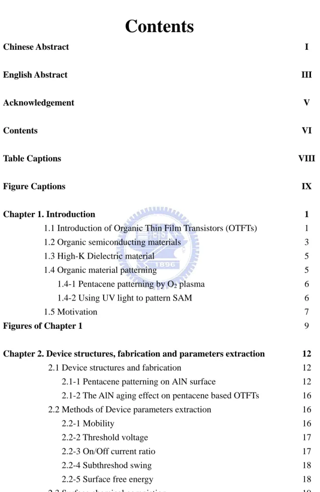
(16) improvement and the choices of materials for the electrodes [5], the insulator [6], the passivations [7], and the substrates [8] are also important factor.. 1-2 Organic semiconducting materials Organic conjugated materials used in OTFTs can be generally divided into two groups. Among the semiconductors, one group is the polymers and the other is the oligomers. The polymers are formed by a repeating chain of hydrogen and carbon in various configurations with other elements, but they have relatively poor mobility (4×10⁻² cm2/Vs [9]). The oligomers are held tighter by weak Van der Waal forces and thermal-evaporated with good ordering. Devices fabricated with oligomers have higher mobility (1.5 cm2/Vs) [10]. Organic materials such as polythiophene, α-sexithiophene (α-6T) have been investigated for use in field effect transistors (FETs) [11].As the chemical formula shown in fig. 1.1 [13], polycrystalline molecular solid, amorphous/semi-crystalline polymers or acenes all show a high mobility in organic based devices[12]. Figure 1.2 shows the evolution of organic materials and the improvement in their mobility over these years [14]. The pentacene (C22H14) is a promising candidate for future electronic devices and an interesting model system, due to its superior field effect mobility and environmental stability [15]. The mobility in pentacene based devices has reached the. 3.
(17) fundamental limit (>3 cm2/Vs) [16] which is obtained with a single crystalline at room temperature. As shown in fig. 1.1(a), pentacene (C22H14) is an aromatic compound with five condensed benzene rings. Its purity leads to longer diffusion length for the charge transporting with less interaction with the lattice. Furthermore, the impurities in the material tend to chemically combine with the organic semiconductor material which leads to irregularities in the band gap [17]. Therefore, the thermal evaporation is carried out under high or ultra high vacuum conditions to avoid the impurities and increase the quality of the material. It is well known that the deposition temperature, deposition pressure, and deposition rate are three critical parameters to the organic film quality. Low deposition rate and appropriate deposition temperature is expected to result in better ordering of the organic molecules, thin-film phase formation of pentacene film, and the better performance [18]. The roughness has an influence on the morphology whereas the films on the smooth thermal oxide are in generally highly ordered. The surface chemistry also is a typical issue. Changing surface polarity as a hydrophobic surface by surface treatment leads to mobility increasing [19].. 4.
(18) 1-3 High-K Dielectric material Organic transistors remain a limitation on their high operating-voltage. To lowering the operating-voltage, using a thinner gate-dielectric [20] or using a high-k gate-dielectric to enhance the capacitance [21] are well known methods. Among the high-k materials, the group III nitrides, aluminum nitride (AlN), has been proposed as a low operating-voltage gate-dielectrics in pentacene based OTFTs. [22] The AlN film is known to have high chemical and physical stability, as well as high dielectric permittivity [23]. For pentacene based OTFTs applications, the AlN dielectric can be fabricated at low temperature (~150°C) using RF-sputtering system and has similar surface energy to the pentacene to let the pentacene film growth well [22].. 1-4 Organic material patterning To reduce drain leakage current and lower crosstalk among devices, pentacene active layers were highly demanded to be patterned. For the applications in organic displays, several pentacene patterning methods were suggested such as, traditional photo resist patterning [24], using water-based photo resist [25] [26], shadow mask patterning [27], and alternative patterning [28] [29]. However, there are still some problems in these patterning methods. In traditional photo resist, the organic film would be destroyed in the solvent based photo resist processes. As shown in fig. 1.3,. 5.
(19) using water-based photo resist (PVA) could reduce the damage of organic film, but the temperature of PVA baking may cause the device degradation. The shadow mask patterning method was widely used in the various processes, but the resolution is limited and it is difficult to apply the method over a large area. Figure 1.4 show the alternative patterning method process, this method didn’t use any solvent, but the pentacene growth and higher off current still need to explore further. Therefore, some patterning methods were published by the modulation of the surface energy. Pentacene grown on the different surface energy would have the different morphology and characteristics. Two of the pentacene patterning by modifying the surface energy was introduced as below:. 1.4-1 Pentacene patterning by O2 plasma [30] O2 plasma and SAM-OTS was used to modify the surface energy by Jin Jang et.al. As illustrated in fig. 1.5, the pentacene film would selective grow on the OTS treatment region. The morphology of the pentacene film would be different when the pentacene film grown on different surface energy region.. 1.4-2 Using UV light to pattern SAM [31] The self-assembled monolayer (SAM) was self-aligned to the gate electrode. 6.
(20) initially formed on the quartz-glass substrate and patterned by the UV light exposure as shown in fig 1.6. The surface polarity of SAM increased drastically when the SAM-treated dielectric surface was exposed by UV light. Different pentacene ordering and electrical characteristic would be observed when the pentacene was grown on the different surface energy region. However, the pentacene was not lifted-off in this method and the drain leakage might be occurred.. 1-5 Motivation In order to fabricate a high performance OTFT, there are still some technologies have to be improved, such as active region patterning, high operation voltage and the influence of aging effect on dielectrice surface. In this thesis, we reported a pentacene patterning method that can be combined with conventional lithography process to pattern pentacene film. The high-k material, AlN film, was used as the gate dielectric. The dielectric surface was patterned using a conventional photo lithography process and then treated with oxygen (O2) plasma on uncovered AlN to modify surface polarity. The O2 plasma treated AlN surface was also analyzed using x-ray photoelectron spectroscopy (XPS) before pentacene deposition. The surface chemistry of the AlN film and the intrusion energy of water were introduced to explain the water-removable pentacene patterning mechanism.. 7.
(21) Otherwise, the relationship between the aging effect on the AlN surface and the OTFTs performance was also demonstrated in this thesis. This surface energy varied over the aging time was observed. The carrier transport in OTFTs was improved when the gate dielectric provided a low surface free energy that matched the organic film. The pentacene growth on the surface with low surface energy was proposed to have a high device performance. The detail relationship between the aged AlN surface and the device performance was demonstrated in this thesis.. 8.
(22) Figures of Chapter 1. Fig. 1.1. Molecular structure of (a) α-sexithiophene (α-6T) (b) pentacene (c) polythiophene.. Fig. 1.2. Semilogarithmic plot of mobility over years.. 9.
(23) Fig. 1.3. The process flow of related patterning method by water-based PVA.. Fig. 1.4 The process flow of alternative method. 10.
(24) Fig. 1.5. The cross-section of related patterning method by O2 plasma.. Fig. 1.6 The process flow of related patterning method by UV light. 11.
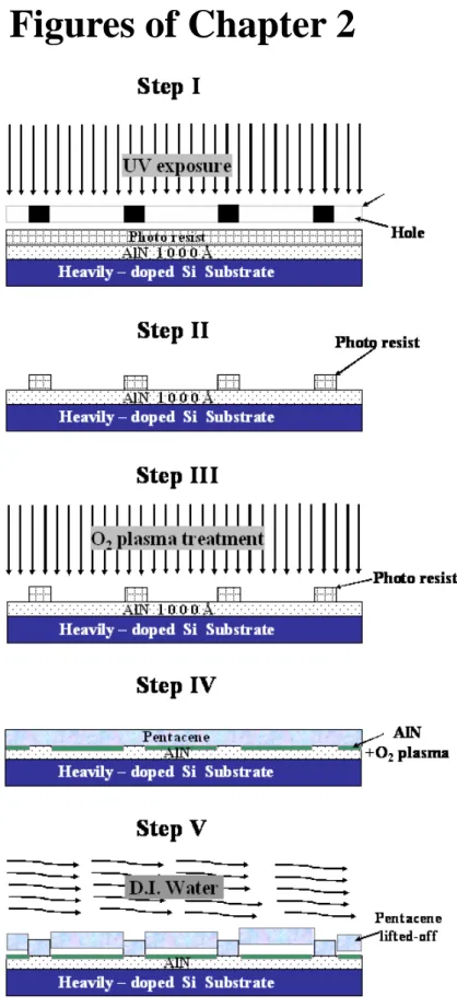
(25) Chapter 2 Device structures, fabrication and parameters extraction 2-1 Device structures and fabrication In this section, the device structure and the process flow of the pentacene based OTFTs on the AlN dielectric were demonstrated. Pentacene patterning methods that was combined with conventional lithography on AlN surface was reported in section 2-1.1. In section 2-1.2, the pentacene based OTFTs was fabricated to observe the relationship between the aging effect on AlN dielectric and the OTFTs performance. The detail fabrication processes are listed as following:. 2.1-1 Pentacene patterning on AlN surface 1. Substrate and gate electrode As shown in fig. 2.1, a 4-inch n-type heavily-doped single crystal silicon wafer with (100) orientation is used as substrate and gate electrode for fabricating a top-contact pentacene based OTFTs. Then, standard RCA clean was used to remove the insoluble organic, ionic and heavy metal atomic contaminants on the silicon substrate surface.. 12.
(26) 2. AlN dielectric deposition After standard RCA cleaning, the 1000 Å aluminum nitride films were deposited by a radio frequency (RF) system [22] [32]. Before the AlN film deposition, the n+-Si wafer was rinsed in de-ionized water (D.I. water), and was then immersed in acetone with ultrasonic to remove the particles and impurities. To remove native oxide on the n+-Si wafer, the wafer was dipped in the dilute HF solution (HF:H2O=1:100). Finally, the cleaned wafer was transferred to the RF-sputtering system chamber immediately. Before admitting gas in, the RF-sputtering system was pumped down to a base pressure less than 2×10⁻⁶ Torr. A mixed argon and nitrogen was monitored by mass flow controllers (MFC) at Ar/N2 ratio 2/9. The AlN film was deposited at a total pressure of 2.5 mtorr at a substrate temperature around 150oC, and RF power was 30W. All relevant experimental details have been published elsewhere [22] [32].. 3. O2 plasma treatment To pattern the pentacene film on the AlN surface, the surface polarity was partial modified using O2 plasma. Before the O2 plasma treatment, the AlN film surface was partially capped and defined using conventional photolithography technology in Step II in fig. 2.1. The FH-6400 photo resist was spin-coating on the AlN surface with fixed pre-spin speed 1000 rpm for 10 seconds, and followed by casting-spin speed. 13.
(27) 4500 rpm for 30 seconds. After 3 minutes soft-baked at 90oC, the conventional lithography process with exposure energy 300W and exposure time 30 seconds was used to define the plasma treatment region. And then, the wafer was sent for developing, where the exposed photo resist is removed with FHD-5 developer. Finally, after rinsed with D.I. water, 3 minutes hard-baked at 120oC is used to expel the solvent inside the photo resist and ensure that unexposed photo resist adheres to the wafer. In Step III , the sample was transferred to a plasma enhanced chemical vapor deposition (PECVD) system. AlN film surface polarity in the remaining unwanted area was modified using O2 plasma in the PECVD for 10 minutes. The O2 plasma parameters were RF-power 100W, process pressure 650 mTorr, chamber temperature 100 oC, and oxygen gas flow rate 900 standard cubic centimeters per minute (sccm). The polarity of the region treated with O2 plasma was changed from hydrophobic to hydrophilic.. 4. Pentacene film deposition After the AlN film surface was defined and modified, pentacene film was deposited on the entire surface in Step IV. The pentacene material obtained from Aldrich without any purification was directly placed in the thermal coater for thermal. 14.
(28) deposition. It is well known that the deposition pressure, deposition rate, and deposition temperature are the critical parameters to the quality of the organic film [33]. The substrate was heated to 70 oC during the deposition at a base pressure of 3×10⁻⁶ Torr. The thickness of the pentacene film was 1000 Å and the deposition rate was 0.5 Å/sec, monitored by the quartz crystal oscillator. Slower deposition rate is expected to result in smoother and better ordering of the organic molecules. The pentacene was deposited directly without shadow mask.. 5. Pentacene patterning As shown in StepV, to partially lift-off and pattern pentacene film, the sample was dipped in D.I. water. And then, the pentacene film on O2 plasma treated region was removed. Finally, pentacene patterning on the defined AlN surface was completed.. 6. Source/Drain electrode deposition The injection barrier of the OTFT device is determined by the materials of the source and drain electrodes. Materials with large work function are preferred to form Ohmic contact [5]. The Au with work function ~5.1eV does help to provide a better injection. Then, we deposited Au as the source/drain electrodes on the pentacene film.. 15.
(29) The thickness of the Au electrode pad is 1000 Å.. 2.1-2 The AlN aging effect on pentacene based OTFTs The AlN deposition parameters were the same as mentioned in the second part of section 2.1-1. To observe the relationship between the AlN aging effect and pentacene growth mechanism, the AlN samples were stored in a dry box for several days before pentacene film deposited. The humidity in dry box was controlled to lower than 35% under room temperature. The dry box was obtained from Ace Dragon Corporation’s Dr. Storage Series (model AD315). Then, the pentacene film was deposited on the AlN surface and was defined through a shadow mask. The device channel width and length were defined as 1000 μm and 400 μm.. 2.2 Methods of Device parameters extraction In this section, the methods of extraction the mobility, the threshold voltage, the on/off current ratio, the subthreshold swing, the surface free energy is characterized, respectively.. 2.2-1 Mobility Generally, mobility can be extracted from the transconductance maximum gm in the linear region: 16.
(30) ⎡ ∂I ⎤ WCOX gm = ⎢ D ⎥ = μVD L ⎣ ∂VG ⎦VD =const .. (2.1). Mobility can also be extracted from the slope of the curve of the square-root of drain current versus the gate voltage in the saturation region, i.e. − VD > −(VG − VTH ) :. ID =. W μCOX (VG − VTH ) 2L. (2.2). 2.2-2 Threshold voltage Threshold voltage is related to the operation voltage and the power consumptions of an OTFT. We extract the threshold voltage from equation (2.2), the intersection point of the square-root of drain current versus gate voltage when the device is in the saturation mode operation.. 2.2-3 Ion/Ioff current ratio Devices with high Ion/Ioff ratio represent large turn-on current and small off current. It determines the gray-level switching of the displays. High on/off current ratio means there are enough turn-on current to drive the pixel and sufficiently low off current to keep in low power consumption.. 17.
(31) 2.2-4 Subthreshod swing Subthreshold swing is also important characteristics for device application. It is a measure of how rapidly the device switches from the off state to the on state in the region of exponential current increase. Moreover, the subthreshold swing also represents the interface quality and the defect density [34].. S=. ∂VG ∂ (log I D ). VD = const .. , when VG < VT for p-type.. (2.3). If we want to have good performance TFTs, we need to lower subthreshold swing of transistors.. 2.2-5 Surface free energy The contact angle measurements were used to study migration of hydrophobic and hydrophilic functional groups. The water Contact angle was sensitive to film surface chemical composition [35]. The contact angle was obtained by the KRŰSS Contact Angle System for universal surface testing (model GH-100). Three standard liquids (D.I. water, diiodo-methane and ethylene glycol) were applied to measure the contact angles and thus extract the material surface energy. Then, surface energy was calculated using Fowkes and Young approximation, as in the following equation; [36] [37]. (1 + cos θ )γ L = 2(γ Sd γ Ld )1/ 2 + 2(γ Spγ Lp )1/ 2 18. (2.4).
(32) where θ was the measured contact angle; γ L was the tested liquid surface energy and is the sum of its dispersion γ Ld and polar part γ Lp ; γ Sd and γ Sp are the dispersion and polar components, respectively, of solid surface free energy. The contact angles of three standard liquids (D.I. water, diiodo-Methane and ethylen glycol) were measured to obtain values of γ Sd and γ Sp . The γ Ld and γ Lp values of these standard liquids were used to calculate the γ Sd and γ Sp values of the dielectric surface. Also, the total surface free energy of solid γ S was estimated by using. γ S ≅ γ sp + γ sd. (2.5). All relevant surface energy details have been analyzed elsewhere [38].. 2.3 Surface chemical composition Surface composition and chemical bonding states were investigated using XPS (ESCA PHI1600). X-ray radiation was provided by a monochromated Mg anode Kα line at 1253.6 eV. The base pressure of the instrument was 5×10⁻⁹ torr. The C 1s at 284.5 eV was used as a reference for all detected peak positions. To separate chemical bonding states in the ESCA spectra, the spectral line shape was simulated using a suitable combination of Gaussian and Lorentzian functions.. 19.
(33) Figures of Chapter 2. Fig. 2.1 Schematic showing the proposed pentacene patterning process.. 20.
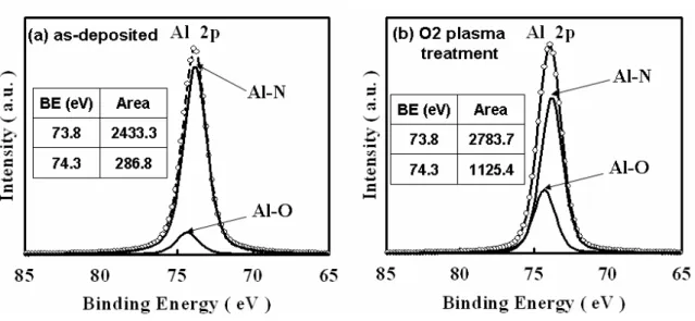
(34) Chapter 3 Result and Discussion 3.1 Pentacene Patterning 3.1-1 Surface energy control The surface polarity of AlN film was hydrophobic .With 10 minutes O2 plasma treatment, the contact angle and surface free energy variation of the AlN film was shown in Table I. The contact angle of AlN film varied from 81.7o to 3.3o and the surface free energy varied from 53 mJ/m2 to 161.2 mJ/m2. It implied the AlN film transferred from hydrophobic to hydrophilic surface. The surface free energy of AlN film was increased drastically after O2 plasma treatment. Oxygen (O2) and oxygen-containing plasmas are well known to produce a variety of oxygen functional groups and to modify surface energy [39]. This high/low surface difference controlled by O2 plasma treatment was an important factor for further pentacene patterning.. 3.1-2 Surface Chemistry of the AlN film To understand the surface chemistry of AlN film treated with O2 plasma, the AlN surfaces were characterized using XPS. As shown in fig. 3.1~3.3, XPS spectra of N 1s, Al 2p, and O 1s core levels from the AlN surface treated with/without O2 plasma. The N 1s core level from the as-deposited AlN surface was approximately 398.3 eV in the. 21.
(35) binding energy scale as shown in fig. 3.1(a). A small peak at approximately 402.8 eV -. next to the N 1s peak was the azide ( N 3 ) peak [40]. The existence of azide in AlN resulted from the incomplete dissociation of nitrogen in low power plasma operation conditions. Both N 1s and azide peaks were also observed for the O2 plasma treated AlN surface as shown in fig. 3.1(b). The N 1s intensity remains unchanged. However, the azide peak became weaker. This may be due to the reduction of the azide group by gaining electrons from the plasma to the electron-deficient nitrogen. Figure 3.2(a) shows the Al 2p core level from the as-deposited AlN surface. The as-deposited AlN surface was partially oxidized since the O 1s signal also appears in the XPS spectrum as shown in fig. 3.3(a). The partially oxidized AlN surface was expected since the as-deposited AlN surface was exposed to air before the pentacene deposition. The curve-fit data in fig. 3.2(a) indicate that the Al 2p signal consists of an Al-O peak at 74.3 eV and a pure Al-N peak at 73.8 eV. [41] The ratio of Al-O to Al-N increased when the as-deposited AlN surface was treated with O2 plasma for 10 minutes, as shown in the curve-fit spectra of Al-N and Al-O in fig. 3.2(b). This was attributed to the oxidation of AlN film near the surface in the O2 plasma bombardment process. O2 plasma oxidation is further confirmed by the increase of O1s signal, according to the relative peak area of O 1s in figs. 3.3(a) and 3.3(b). The increase of the ratio of Al-O to Al-N made the AlN surface more polar since the polarity of Al-O was higher than. 22.
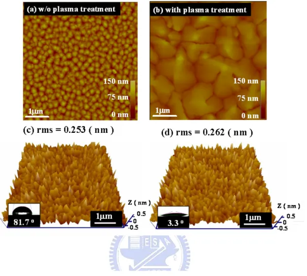
(36) that of Al-N. The AlN surface thus became hydrophilic and increased possible reactions with water. This may have played an important role in the lift-off step using water dipping in pentacene patterning.. 3.1-3 Pentacene Morphology After O2 plasma treatment, a pentacene film was evaporated on the AlN surface. Pentacene surface morphology is presented in figs. 3.4(a) and 3.4(b). The Pentacene film on the O2 plasma treated surface showed large and dendrite-like grains. On the other hand, small grains were observed in pentacene film grown on the untreated AlN surface. Pentacene growth can be affected by factors such as surface roughness and surface energy. The effect of surface roughness on pentacene growth has been previously reported [42] [43] [44] [45] [46] [47]. After O2 plasma treatment, surface roughness was altered from 0.253 nm to 0.262 nm as shown in figs. 3.4(c) and 3.4(d). The change of AlN surface roughness was very small after the O2 plasma treatment. Pentacene growth was considered not affected by surface roughness in our study. Sang Yoon Yang et. al. proposed that pentacene grain morphology was affected by surface energy [48]. As shown in figs. 3.4 (c)~(d) insets, the water contact angle decreased from 81.7o to 3.3o after O2 plasma treatment. The relative surface energy. 23.
(37) was derived from the water contact angles using equations (2.4)-(2.5), and listed in Table I. The polar and dispersive components of the surface energy were also derived and listed in Table I. The surface energy increases after O2 plasma treatment. Note that large grains of pentacene growth on a surface with large surface energy were observed. The increase of pentacene grain size on the plasma treated AlN surface is thus attributed to increase in surface energy.. 3.1-4 Pentacene Patterning Analysis To identify the pentacene patterning mechanism, adhesion energy was used to characterize the adhesive strength of pentacene to different surfaces. The adhesion energy between materials, given by the following equations, has been presented elsewhere [38] [49] [50]: d d Ebefore = 2( γ pep γ sp + γ pe γs ). (3.1). where Ebefore denotes the adhesion energy between pentacene and the substrate before p d dipping in water; γ pe and γ pe are the polar and the dispersion components of the. p d pentacene surface energy, and γs and γs. are the polar and the disperse. components of the substrate surface energy. The calculated adhesion energy is summarized in Table II. The adhesion energy Ebefore between the pentacene film and the O2 plasma treated AlN surface is larger than the untreated surface. The increase in. 24.
(38) adhesion energy is not consistent with water-removable characteristics. Generally, higher adhesion is achieved when an organic film is deposited on a higher polar substrate. [51] The Al 2p XPS spectra presented in figs. 3.2(a) and 3.2(b) and the O 1s spectra in figs. 3.3(a) and 3.3(b) can be used to explain higher adhesion energy. The higher polar surface was obtained according to the enhanced Al-O bonding signal after O2 plasma treatment. These results were consistent with the higher polar component of surface energy after O2 plasma treatment as listed in Table I. Intrusion energy EI was calculated to confirm the water-removable characteristics. Intrusion energy is caused by the interaction of water, pentacene and the AlN surface. The adhesion energy is affected by the intrusion energy EI according to the equation:. E after = Ebefore − E I. (3.2). where Eafter denotes the adhesion energy after dipping in water. The intrusion energy EI is calculated using the following equation:. [. d E I = 2{ γ sop γ sp + γ sod γ sd + γ pep γ sop + γ pe γ sod − γ sop + γ sod. p where γ so. and. ]}. (3.3). d γ so are the polar and disperse components of the surface energy. of the dipping solution (D.I. water). Table II lists the calculated intrusion energy EI and the adhesion energy after dipping in water, i. e. Eafter. EI increases significantly after the O2 plasma treatment. Consequently Eafter decreases to less than zero after the. 25.
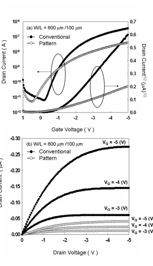
(39) O2 plasma treatment. Specifically, the Eafter of the untreated region is 51.5 mJ/m2 and that of the treated region is -38.5 mJ/m2. This fact explains the experimental results in fig. 3.5(b). The pentacene on the untreated area was almost unaffected because Eafter was large; the pentacene film on the area that had been treated by O2 plasma was removed by dipping in water because Eafter became negative. Also, the large difference between the Eafter of the untreated area and that of the treated area completely explain pentacene patterning capacity. Higher polar surfaces can more easily react with polar solutions, which have been reported in previous studies [52] [53] [54]. The interface of the pentacene film and a higher polar AlN surface reacts more easily with D.I. water during water dipping. This result was consistent with the higher intrusion energy (140 mJ/m2) on the O2 plasma treated surface when the interface was dipped in D.I. water. The high intrusion energy associated with high polar surface energy of the O2 plasma treated AlN surface explained the water-removable pentacene patterning mechanism.. 3.1-5 Device Characteristic The electronic characteristics were demonstrated to confirm that the patterning scheme was feasible for the OTFTs or not. All electrical characteristics were measured using Agilent 4156 and Agilent 4284 analyzers. Figure 3.6 (a) and (b). 26.
(40) compares the transfer characteristics (ID-VG) and output characteristics (ID-VD) of OTFT under the proposed patterning methods. Table III lists the typical parameters such as mobility, threshold voltage, Ion /Ioff current ratio, subthreshold swing and the extracted interface state density ( Nss ). The mobility and threshold voltage were extracted by the slope and the intercept of the square root of ID versus VG plot in fig. 3.6. The interface state density was extracted by the method proposed in [34]. Compare to the devices patterned by the shadow mask, OTFTs fabricated by the proposed patterning methods exhibited a worse mobility, subthreshold swing and interface state density. The bad performance in OTFTs fabricated by the proposed methods may be due to the damage in AlN dielectric film by the D.I. water, photo resist or the high power O2 plasma treatment. Some residual water molecules from the water dipping process may have been responsible for the slight increase in the the off-state current and the subthreshold swing, which phenomenon must be further studied.. 3.2 The AlN aging effect on pentacene based OTFTs 3.2-1The AlN aging effect on device characteristics Aging effect on the AlN dielectric was observed in pentacene based OTFTs. Pentacene based OTFTs were deposited on the AlN dielectric surfaces which were. 27.
(41) stored in a dry box for various aging times. The electronic characteristics confirmed the relationship between the OTFTs performance and the AlN dielectric aging effect. Figure 3.7(a) compares the transfer characteristics (ID-VG) of OTFTs fabricated on the as-deposited AlN surfaces and on the AlN surfaces, which were aged for 14 days. Table IV lists the typical OTFT parameters such as field effect mobility (μFE), threshold voltage (VTH), subthreshold swing (S.S), Ion/Ioff current ratio and the extracted interface state density (NS.S.). All the electrical characteristics were measured by Agilent 4156 and Agilent 4284 analyzers. As shown in fig. 3.7(a), OTFTs fabricated on the AlN surface which was aged for 14 days markedly outperformed OTFTs on the as-deposited AlN surface. A steep subthreshold characteristic (S.S.), a high field effect mobility (μFE) of the saturation region and a low interface trap density (NS.S.) were obtained. Figure 3.7(b) plots the output characteristics (ID-VD) of OTFTs samples. Higher output current was observed when OTFTs fabricated on the AlN surface aged for 14 days. As shown in fig. 3.8(a), field effect mobilities were compared with OTFTs fabricated on AlN surfaces aged at various time. Higher field effect mobilities were obtained with pentacene based OTFTs fabricated on aged AlN surfaces. The mobility increased with the AlN surface aging time. OTFTs fabricated on the 14 day AlN surface appeared the highest mobility of 0.67 cm2/Vs. Carrier transport in pentacene-based OTFTs is generally. 28.
(42) dominated by interface characteristics between pentacene film and the gate dielectric [55].. Defects in thin film or on the dielectric and organic active-layer interface will. affect carrier transport and degrade carrier mobility. The subthreshold characteristics (S.S.) and the extracted interface trap density of OTFTs fabricated on the aged AlN surface with various aging times were plotted in 3.8(b). The OTFTs subthreshold swing and the extracted interface trap density were decreased over AlN aging time when OTFTs was fabricated on the aged AlN surface. These results were consisted with enhanced mobility over the AlN aging time. Carrier transport was improved when the pentacene based OTFTs was fabricated on the aged AlN surface. The improved electrical characteristics are attributed to the pentacene growth mechanism which will be characterized and discussed in the following sections.. 3.2-2 Surface free energy with various AlN aging time Numerous studies of low dielectric surface energy have been performed to improve carrier mobility [55] [56] [57]. The researchers found that hydrophobic dielectrics provide a low surface-energy interface that matched the organic thin film. Defects degrading carrier transport in thin film or on the dielectric and organic active-layer interface were reduced. The hydrophobic surface (low surface energy) enables pentacene molecules to align vertically to form the π-orbital and improve. 29.
(43) electrical characteristics. As shown in fig. 3.9(a), the circle symbols represent the water contact angle on the AlN surface over various aging times. The water contact angle was approximately 38.3 degrees on an as-deposited AlN surface and 79.2 degrees on a 14 days AlN surface. The water contact angle increased over aging time. The variation in the contact angle represented the change in surface energy. These liquid contact angles, diiodo-methane and ethylene glycol, were also measured and shown in fig. 3.9(a) to extract the surface energy. Figure 3.9(b) presents the surface energy calculated results. When aging time increased, the surface energy was lowered. The lowered surface energy over aging time was due to carbon absorption. The carbon was attributed to atmosphere during sample transfer and storage.. 3.2-3 Surface chemistry of the aged AlN film To understand the surface chemistry of carbon absorption on aged AlN surface, the AlN surfaces were characterized using XPS. XPS spectra of C 1s core level from the as-deposited and 14 day AlN surfaces are shown in figs. 3.10(a) and 3.10(b). The curve-fit data in figs. 3.10(a) and 3.10(b) indicate that the C 1s signal consists of an C=C peak at 284.5 eV, an C-O peak at 286.7 eV and an O-C=O peak at 288.5 eV [58] [59] [60]. An increased C=C peak intensity was observed on the aged 14 days AlN. 30.
(44) surface. The enhanced C=C peak at 284.5 corresponds to C 1s, suggesting that carbon is the only major element on the AlN surface. Some similar results in tin-doped indium oxide (ITO) research have also been reported [61] [62] [63]. The enhanced carbon absorption on the AlN surface made the surface hydrophobic and lowered surface energy. Otherwise, the signal of oxidized carbon components, C-O and O-C=O, were reduced. The weaker signal of the polar functional groups, C-O and O-C=O, consisted of a reduced polar component surface energy. The enhanced C=C peak plays an important issue in affecting pentacene growth. Like the substrate surface treated with a self-assembled monolayer (SAM) before pentacene growth, the C=C signal on the substrate surface was enhanced and the performance of pentacene based OTFTs was also increased [38] [64] [65]. The lowered surface energy on the aged AlN surface was due to the increased C=C peak intensity and lowered polar functional groups.. Pentacene growth and morphology may be affected when. pentacene grown on a surface with different surface characteristics.. 3.2-4 Pentacene morphology Figure 3.11 presents the AFM images of pentacene deposited on the AlN surface. The AFM image was obtained by the tapping mode using an AFM model Dimension 3100, Digital Instrument. Pentacene growth can be affected by factors such as surface. 31.
(45) roughness and surface energy. The effect of surface roughness on pentacene growth has been previously reported [42] [43] [44] [45] [46] [47]. The AlN surface roughness did not obviously vary after being aged for 14 days. The surface roughnesses of all AlN surfaces were kept at 0.24 ± 0.02 nm. The change of AlN surface roughness was very small after 14 days of aging. Pentacene growth was not affected by surface roughness in this study. Figures 3.11(a) and (b) were the morphology of very thin (3-9 nm) pentacene film on the as-deposited AlN surface and the aged 14 days AlN surface. The AFM images demonstrate that the pentacene deposited on the aged 14 days AlN surface had larger coverage on the first few monolayer. This kind of initial growth was described by the Stranski-Krastanov growth mode [66]. In contrast, the Volmer-Weber growth mode was also observed on as-deposited AlN surface [66]. Pentacene coverage on the as-deposited AlN surface was about 29% and on the aging 14 days AlN surface was around 53%. High pentacene coverage in the first few layers showed high OTFTs performances which were proposed by Kelley et al [67] [68]. The pentacene voids were formed easier when the first few pentacene layers had lower coverage. The voids and successive incomplete layers over the first few pentacene layers limited carrier transport and decreased carrier mobility [69]. It was reported that voids and successive incomplete layers could be reduced when pentacene was deposited on a low surface energy gate dielectric or a low polar energy. 32.
(46) surface [69]. These results are consisted with the surface energy and mobility reported in section 3.2-1 and 3.2-2. AFM images of 1000-Å-thick pentacene deposited on as-deposited AlN surface and the aged 14 days AlN surface are shown in figs. 3.11(c) and (d). Large and dendrite-like grains were observed in pentacene film grown on all of the AlN surfaces. The relationship between the morphology of 1000-Å-thick pentacene film and device performance was not obvious because the difference in pentacene grain sizes were not large enough. Thus, further research about the details relating to grain size of thick pentacene on the AlN surface and OTFTs performance is under investigation.. 33.
(47) Figures of Chapter 3. Fig. 3.1 XPS spectra of (a) N 1s core levels from the as-deposited AlN surface and (b) N 1s core levels from the O2 plasma treated AlN surface. The energy position and peak area of the curve-fit data are listed in the inserted table.. Fig. 3.2 XPS spectra of (a) Al 2p core levels from the as-deposited AlN surface and (b) Al 2p core levels from the O2 plasma treated AlN surface. The energy position and peak area of the curve-fit data are listed in the inserted table. 34.
(48) Fig. 3.3 XPS spectra of (a) O 1s core levels from the as-deposited AlN surface and (b) O 1s core levels from the O2 plasma treated AlN surface. The energy position and peak area of the curve-fit data are listed in the inserted table.. 35.
(49) Fig. 3.4. AFM images showing pentacene on (a) the as-deposited AlN surface and on (b) the O2 plasma treated AlN surface. The AFM images of surface roughness of (c) the as-deposited AlN surface and (d) the O2 plasma treated AlN surface. The corresponding optical micrograph of the water contact angle on the AlN surface is inserted in the lower-left corner. The surface height is expressed on the z-axis scale. The surface height is expressed by the relative contrast in the AFM images.. 36.
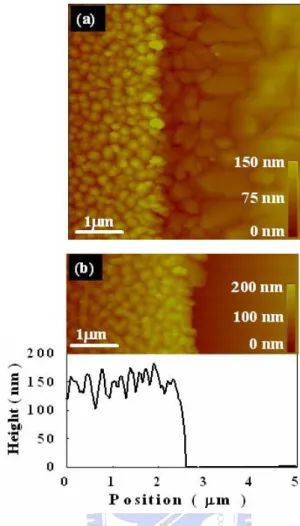
(50) Fig. 3.5. (a) AFM image showing the pentacene morphology .The grain size of pentacene is larger on the AlN treated with O2 plasma. (b) The pentacene on the AlN treated with O2 plasma is removed by water dipping. The measured height difference is ~ 150 nm which implies that the pentacene film was completely removed.. 37.
(51) Fig. 3.6. (a) Transfer characteristics (b) Output characteristics of the conventional and patterned OTFTs.. 38.
(52) Fig. 3.7. (a) The transfer characteristics of OTFTs fabricated on the as-deposited and 14 day aged AlN surface. The square roots of ID versus VG on the respective samples plotted on the right y-axis. (b) The output characteristics of OTFTs fabricated on the respective AlN surface.. 39.
(53) Fig. 3.8. The plotted of OTFT device performance. (a) Field effect mobility versus aging time (b) Subthreshold swing and interface trap density versus various aging times.. 40.
(54) Fig. 3.9. (a) Contact angle of AlN surface versus various aging times. (b) Surface free energy of AlN versus various aging times. The gray symbol was the measured data of 1 month aged AlN surface.. 41.
(55) Fig. 3.10 XPS spectra of (a) C 1s core levels from the as-deposited AlN surface and (b) C 1s core levels from aging 14 days AlN surface. The energy position and peak area of the curve-fit data are listed in the inserted table.. 42.
(56) Fig. 3.11. (a) The morphology of pentacene on as-deposited AlN film and on (b) the 14 days aged AlN surface in the first few monolayers. (c) The morphology of pentacene on as-deposited AlN film (d) aging 14 days about 100 nm thicknesses.. 43.
(57) w/o O2 plasma treatment. with O2 plasma treatment. Water contact angle (degree). 81.7. 3.3. Surface Energy γs (mJ / m2). 53. 161.2. Polar component γ S (mJ / m2). 13.2. 114.4. Disperse component γ S (mJ / m2). 39.8. 46.8. p. d. Table I. Water contact angles and the corresponding surface energies of the as-deposited AlN surface and the O2 plasma treated AlN surface.. w/o O2 plasma treatment. with O2 plasma treatment. Adhesion energy Ebefore (mJ / m2). 86.1. 101.9. (mJ / m2). 34.5. 140.4. Adhesion energy Eafter (mJ / m2). 51.5. -38.5. Intrusion energy EI. Table II. Intrusion energy and adhesion energy between the pentacene film on the AlN surface in various experimental conditions.. 44.
(58) Table III. Extracted parameters of conventional and patterned OTFTs.. Table VI. Extracted parameters of OTFTs under various AlN aging conditions.. 45.
(59) Chapter 4 Conclusion Pentacene patterning on the AlN dielectric surface and the aging effect on AlN surface in pentacene based OTFTs were developed in this thesis. A simple pentacene patterning process has been demonstrated using water dipping. The pentacene was completely lifted-off by water dipping on the area of AlN treated with O2 plasma. The AlN surface treated with O2 plasma becomes more polar after the O2 plasma treatment based on surface energy measurements. The polar surface energy enhanced the intrusion energy of water and helped lift-off the pentacene film on the O2 plasma treated AlN surface. The high intrusion energy associated with high polar surface energy of the O2 plasma treated AlN surface explained the water-removable pentacene patterning mechanism. The simple pentacene patterning process is compatible with conventional lithography and is applicable to future OTFT array processes. The aging effect on the AlN gate dielectric in pentacene based OTFTs were investigated. The relationship between the carbon absorption and the electrical characteristics in pentacene based OTFTs was established. The OTFTs fabricated on the aged 14 days AlN surface with larger carbon absorption have large field effect mobility. The mobility was enhanced from 0.05 cm2/Vs to 0.67 cm2/Vs with the. 46.
(60) limited aging time (14 days). The improved mobility was due to the carbon accumulation on the AlN surface, lowered the surface energy and increased the pentacene coverage in the first few layers. The electrical performance in pentacene based OTFTs is closely related to the carbon accumulation on the dielectric surface. The carbon accumulation issues must be considered when developing process for preparing pentacene based OTFTs and other interface sensitive devices.. 47.
(61) Reference. [1] H. Shirakawa, E. J. Louis, A. G. MacDiarmid, C. K. Chiang, and A. Heeger, “Synthesis of electrically conducting organic polymers: Halogen derivatives of polyacetylene, (CH)x”, J. Chem. Soc. Chem. Commun, Vol. 00, pp. 578, (1977). [2] A. Tsumura, H. Koezuka, and T. Ando, “Macromolecular Electronic Devices: Field-Effect Transistor with a Polythiophene Thin Film”, Appl. Phys. Lett. Vol.49, pp. 1210, (1986). [3] G. Horowitz, D. Fichou, X. Peng, Z. Xu, and F. Garnier, “A Field-Effect Transistor Based On Conjugated Alpha-Sexithienyl”, Solid State Commun. 72, 381 (1989). [4] Lee S, Koo B, Shin J, E Lee, Park H. and Kim H. 2006 Appl. Phys. Lett. 88 162109. [5] C.W. Chu, S.H. Li, C.W. Chen, V. Shrotriya, Y. Yang, “High-performance organic thin-film transistors with metal oxide/metal bilayer electrode” , Applied Physics Letters, Vol. 87, pp.193508, (2005). [6] K. Puntambekar, J. Dong, G. Hangstad, C.D. Frisbie, “Structural and electrostatic complexity at a pentacene/insulator interface” , Adv. Funct. Mater, Vol.16, pp.679 (2006). [7] M. Kawasaki, S. Imazeki, M. Ando, Y. Sekiguchi, S. Hirota, “High-resolution full-color LCD driven by OTFTs using novel passivation film”, IEEE Transactions on Electron Devices, Vol. 53, pp. 435- 441, (2006). [8] K. Tsukagoshi, J. Tanabe, I. Yagi, K. Shigeto, “Organic light-emitting diode. 48.
(62) driven by organic thin film transistor on plastic substrates”, Journal of Applied Physics, Vol. 99, pp.064506. [9] Z. Bao, A. Dodabalapur, A. J. Lovinger, “Soluble and processable regioregular poly(3-hexylthiophene) for thin film field-effect transistor applications with high mobility” Appl. Phys. Lett. Vol. 69, pp.4108, (1996). [10] Y. Y. Lin, D. J. Gundlach, S. Nelson, T. N. Jackson, “Stacked pentacene layer organic thin-film transistors with improved characteristics”, IEEE Electron Device Lett, Vol. 18, pp.606, (1997). [11] L. Torsi, A. Dodabalapur, L. J. Rothberg, A. W. P. Fung, H.E. Katz, “Performance Limits of Organic Transistors”, Science, 1996, P 1462. [12] H. E. Katz, C. Kloc, V. Sundar, J. Zaumseil, A. L. Briseno, Z. Bao, “Field-Effect Transistors made from Macroscopic Single Crystals of Teracene and Related Semiconductors on Polymer Dielectrics”, Journal of Material Research, Vol. 19, No. 7, Jul 2004, P1995-1998. [13] C. Reese, M. Roberts, Mang-mang Ling, and Z. Bao, “Organic thin film transistors”, Materialstoday, Vol. 7, pp. 20-27, (2004). [14] C. D. Dimitrakopoulos, D. J. Mascaro, “Organic Thin-Film Transistors: A Review of Recent Advances”, IBM Journal of Research and Development, Vol. 45, No. 1, Jan 2001, P 11-27. [15] Yanming Sun, Yunqi Liu, and Daoben Zhu, “Advances in organic field-effect transistors”, J. Mater. Chem., vol 15, pp. 53, (2005). [16] G. M. Wang, J. Swensen, D. Moses, and A. J. Heeger, “Increased mobility from regioregular poly (3-hexylthiophene) field-effect transistors”, J. Appl. Phys, Vol 93,. 49.
(63) pp 6137, (2003). [17] Y. S. Yang, S. H. Kim, J. Lee, H.Y. Chu, L. Do, “Deep-level defect characteristics in pentacene organic thin films”, Applied Physics Letters, Vol. 80, pp. 1595-1597, (2002). [18] H. Yanagisawa, T. Tamaki, M. Nakamura, K. Kudo, “Structural and electrical characterization of pentacene films on SiO2 grown by molecular beam” Thin Solid Films, Vol. 464-465, pp.398, (2004). [19] D. Knipp, R. A. Street, A Vo‥ lkel, J. Ho. “Pentacene thin film transistors on inorganic dielectrics: Morphology, structural properties, and electronic transport” Journal of Applied Physics, Vol. 93, pp. 247, (2003). [20] Marcus Halik, Hagen Klauk, Ute Zschieschang, Gunter Schmid, Christine Dehm, Markus Schutz, Steffen Maisch, Franz Effenberger, Markus Brunnbauer, and Francesco Stellacci, Nature (London) 431, (2004) 963. [21] A. –L Deman, J. Tardy, Organic Electronics 6 (2005) 78. [22] Hsiao-Wen Zan, Kuo-Hsi Yen, Pu-Kuan Liu, Kuo-Hsin Ku, Chien-Hsun Chen J ennchang Hwang, J. J. Appl. Phys. 45 (2006) L1093. [23] Laurie Valbin, Laure Sevely, and Serge Spirkovitch, Proceeding of SPIE 4174, (2000) 154. [24] D. J. Gundlach, T. N. Jackson, D. G. Schlom, S.F. Nelson, “Olvent-induced phase transition in thermally evaporated pentacene film”, Applied Physics letters, May, (1999). [25] C. D. Sheraw, L. Zhoy, J. R. Huang, D. J. Gundlach, T. N. Jackson, “Organic. 50.
(64) thin-film transistor-driven polymer-dispersed liquid crystal displays on flexible polymeric substrates”, Applied Physics Letters, Vol. 80, pp1088, (2002). [26] J. W. Kim, “Process temperature dependency on electrical performance of OTFTs in the pattering of a pentacene active layer by PVA photo resistor.” SMDL, Annual Report, (2003). [27] I. Kymissis, C. D. dimitrakopoulos, and S. Purushothaman, J. Vac. Sci. Technol. B 20, 956 (2002). [28] K. H. Kim, K. W. Bong, and H. H. Lee, “Alternative to pentacene patterning for organic thin film transistor” Applied Physics Letters, Vol. 90, pp. 093505, (2007). [29] S.Y. Park, T. Kwon, and H. H. Lee, Adv. Mater. ( Weinheim, Ger.) 18, 1861 (2006). [30] Sung Hwan Kim, Hye Young Choi, Seung Hoon Han, Ji Ho Hur, Jin Jang, “Self-organized organic thin-film transistor for flexible active-matrix display”, SID, pp.1294 (2004). [31] M. Ando, M. Kawasaki, S. Imazeki, “Organic thin-film transistors fabricated with alignment-free printing technique”, Materials Research Society, Vol. 814, (2004). [32] C. -M. Yeh, C.H. Chen, J.-Y. Gan, C.S. Kou, and J. Hwang, Thin Solid Films 483, (2005) 6. [33] C. D. Dimitrakopoulos, A. R. Brown, and A. Pomp, “Molecular beam deposited thin films of pentacene for organic field effect transistor applications”. J. Appl. Phys., vol. 80, pp. 2501, (1996). [34] K. N. Narayanan Unni, Sylvie Dabos-Seignon, and Jean-Michel Nunzi, “Improved performance of pentacene field-effect transistors using a polyimide gate dielectric. 51.
(65) layer”, J. Phys. D: Appl. Phys., vol 38, pp. 1148, (2005). [35] C. M. Chan, Polymer Surface Modification and Characterization (Hanser Gardner, New York, 1994), Chap. 2, p. 35. [36] Drew Myers, Surfaces, Interfaces, and Colloids: Principles and Applications, 2nd Edition, Wiley, New–York NY, 1999, P.430. [37] Fowkes, F. M., J Phys Chem. 67 (1963) 2538. [38]. H. W. Zan, C. W. Chou, and K. H. Yen, Thin Solid Film 516 (2008) 2231.. [39] H. Y. Yu, X. D. Feng, D. Grozea, Z. H. Lu, R. N. S. Sodhi, A.-M. Hor, and H. Aziz, Appl. Phys. Lett., 78 (2001) 2595. [40] D. C. Boyd, R. T. Haasch, D. R. Mantell, R. K. Schulze, J. F. Evans, and W. L. Gladfelter, Chem. of Mater., 1 (1989) 119. [41] J. A. Kovacich, J. Kasperkiewicz, D. Lichtman, and C. R. Aita, J. Appl. Phys. 15 (1984) 2935. [42] K. Shin, S. Y. Yang, C. Yang, H. Jeon, C. E. Park, Org. Electron. 8 (2007) 336. [43] D. Knipp, R. A. Street, A. R. Völkel, Appl. Phys. Lett. 82 (2003) 3907. [44] D. Knipp, R. A. Street, A. R. Völkel, J. Ho, J. Appl. Phys. 93 (2003) 347. [45] S. Steudel, S. D. Vusser, S. D. Jonge, D. Janssen, S. Verlaak, J. Genoe, P. Heremans, Appl. Phys. Lett. 85 (2004) 4400. [46] S. E. Fritz, T. W. Kelley, C. D. Frisbie, J. Phys. Chem. B 109 (2005) 10574.. 52.
(66) [47] K. Shin, C. Yang, S. Y. Yang, H. Jean, C.E. Park, Appl. Phys. Lett. 88 (2006) 072109. [48] Sang Yoon Yang, Kwonwoo Shin, Chan Eon Park, Adv. Mater. 15 (2005) 1806. [49] Hitoshi Nagata and Akira Kawai, Jpn. J. Appl. Phys. 28 (1989) 2137. [50] D. H. Kaelble, J. Appl. Polym. Sci. 18 (1974) 1869. [51] C. M. Chan, Polymer Surface Modification and Characterization (Hanser Gardner, New York, 1994), Chap. 6, p. 261. [52] C. M. Chan, Polymer Surface Modification and Characterization (Hanser. Gardner,. New York, 1994), Chap. 6, p. 237. [53] C. J. Huang and W. C. Shih, J. Electron. Mater. 32 (2003) 478. [54] C.C. Yeh, Y.J. Lin, S. K. Lin, Y. H. Wang, S. F. Chung, L. M. Huang, and T.C. Wen, J. Vac. Sci. Technol. B 25 (2007) 1635. [55] Iwao Yagi, Kazuhito Tsukagoshi, Yoshinobu Aoyagi, Appl. Phys. Lett., 86 (2005) 103502. [56] M. McDowell, I. G. Hill, J. E. McDermott, S. L. Bernasek, J. Schwartz, Appl. Phys. Lett. 88 (2006) 073505. [57] A. Inoue, T. Ishida, N. Choi, Appl. Phys. Lett. 73 (1998) 14. [58] A. Zhu, M. Zhang, J. Wu, J. Shen, Biomaterials 23 (2002)4657.. 53.
(67) [59] G.J. Fleming, K. Adib, J.A. Rodriguez, M.A. Barteau, J.M. White, H. Idriss, Surf. Sci. 602 (2008) 2029. [60] A. M. Shanmugharaj, S. Sabharwal, A. B. Majali, V. K. Tikku, A. K. Bhowmick, J. Mater. Sci. 37 (2002)2781. [61] M.J. Alam, D.C. Cameron, Thin Solid Films 377–378 (2000) 455. [62] J.A. Chaney, P.E. Pehrsson, Appl. Surf. Sci. 180 (2001) 214. [63] J. Zhang, J. Hu, Z.Q. Zhu, H. Gong, S.J. O’Shea, Colloids Surf. A 236 (2004). [64] W.Y. Chou, C.W. Kuo, Y.S. Mai, S.T. Lin, H.L. Cheng, Proceedings of SPIE 5522 (2004) 97. [65] H Sugimura, N Saito, N Maeda, I Ikeda, Y Ishida, K Hayashi, L Hong, O Takai, Nanotechnology 15 (2004) s69-s75. [66] D. L. Smith, Thin-Film Deposition; Principles and Practice, McGraw-Hill, New York 1995, Ch. 5. [67] T. W. Kelley, L. D. Boardman, T. D. Dunbar, D. V. Muyres, M. J. Pellerite, T. P. Smith, J. Phys. Chem. B 107 (2003) 5877. [68] J. X. Tang, C.S. Lee, M.Y. Chan, S.T. Lee, Appl. Surface Sci. (2008) in press. [69] W. Y. Chou, C. W. Kuo, H. L. Cheng, Y. S. Mai, F. C. Tang, S. T. Lin, C. Y. Yeh, J. B. Horng, C. T. Chia, C. C. Liao, D. Y. Shu, Jpn. J. Appl. Phys. 45 (2006) 7922.. 54.
(68) Resume 基本資料: 姓名: 宋和璁 出生日期: 中華民國 72 年 11 月 9 日 住址: 台北市大同區敦煌路 192 號. 學歷: 國立中央大學機械工程學系先進材料與精密製造組(2002.9~2006.6) 國立交通大學顯示科技研究所碩士. (2006.9~2008.8). 論文題目: 氮化鋁於五苯環有機薄膜電晶體上應用之研究 The Application of Aluminum nitride on Pentacene Based OTFTs. 55.
(69)
數據

+7

Outline
相關文件
oBike 標榜「騎到哪、停到哪」,大量放置可 租借的單車,但隨後各地開始出現棄置、違規
▪ 善用括號:腳本中的文字通常是臺詞或旁白,若有無 法單憑文字表達的內容,可以在文字加上括號,進行 畫面的補充敘述。.
由聲波的波形決 定,不同的人及 樂器產生的波形 都不同。.
主要感染硬碟的開 機區 ,電腦開機 時,病毒就會載入 記憶體,伺機感染
[r]
These results may the sample characteristics improved by plasma treatment which reduced defects of surface by fluorine atoms, providing the more stable conducting
This research aims to manipulate surface hydrophilic/hydrophobic properties of Expanded-Polytetrafluoroethylene (e-PTFE) material by RF plasma modification system using O 2 , Ar
再以超音波檢測技術之直接傳遞法如圖 4-14、4-15 進行波速之 量測,其程序是將發射端探頭固定於長梁試體之 15cm*15cm 一 端,接收端探頭置於另一端
