行政院國家科學委員會專題研究計畫 期中進度報告
子計畫四:OFDM FFT 架構下軟體無線電訊號處理之軟、硬體
輔成設計及其數位通信之應用設計(1/3)
計畫類別: 整合型計畫 計畫編號: NSC91-2218-E-009-012- 執行期間: 91 年 08 月 01 日至 92 年 07 月 31 日 執行單位: 國立交通大學電子工程研究所 計畫主持人: 陳紹基 計畫參與人員: 曲建全、洪崇斌、陳坤隆、黃崇倫、葉顏輝 報告類型: 完整報告 報告附件: 出席國際會議研究心得報告及發表論文 處理方式: 本計畫涉及專利或其他智慧財產權,2 年後可公開查詢中 華 民 國 92 年 6 月 2 日
行政院國家科學委員會補助專題研究計畫
期中進度報告
(計畫名稱)
用於軟體無線電基頻處理之系統晶片設計技術-子計畫四:OFDM FFT
架構下軟體無線電訊號處理之軟、硬體輔成設計及其數位通信之應用
設計(1/3)
計畫類別:□ 個別型計畫 █ 整合型計畫
計畫編號:NSC 91-2218-E -009 -012-
執行期間: 91 年 8 月 1 日至 92 年 7 月 31 日
計畫主持人:陳紹基
共同主持人:
計畫參與人員: 曲建全、洪崇斌、陳坤隆、黃崇倫、葉顏輝
成果報告類型(依經費核定清單規定繳交):□精簡報告 █完整
報告
本成果報告包括以下應繳交之附件:
□赴國外出差或研習心得報告一份
□赴大陸地區出差或研習心得報告一份
□出席國際學術會議心得報告及發表之論文各一份
□國際合作研究計畫國外研究報告書一份
附件一處理方式:除產學合作研究計畫、提升產業技術及人才培育研究
計畫、列管計畫及下列情形者外,得立即公開查詢
□涉及專利或其他智慧財產權,□一年□二年後可公
開查詢
摘要
在這個計劃中已經得到了五個進展成果。第一個部分是關於可變長度的快速 傅利葉轉換處理器所使用的資料位址產生器設計;另一方面,對於傅利葉轉換中 所需要的旋轉因數指標產生器亦是可變長度快速傅利葉轉換處理器中的重要設 計,在這裡共有二個用於固定基數演算法與一個用於分裂基數演算法的旋轉因數 指標產生器設計將會在第二部分提出。為了減少儲存旋轉因數所佔用的硬體成 本,第三部份會介紹一個以遞迴方程式來產生正弦與餘弦函數的旋轉因數產生器 設計。第四部份是一個範例性質的可變長度快速傅利葉轉換處理器整合實作。最 後一部份是一個結合 DCT 技術設計出之一新的高效能之 OFDM 通道估測演算 法。Abstract
There are five intermediate results generated so far from our on-going project. The first four results are related to the IFFT processor design for the demodulation of OFDM-based wireless/wireline communication systems including DAB, DVB, 802.11a, 802.16 and VDSL systems. The four IFFT related results are: (1) a data address generator designed for memory-based, variable-length FFT processor; (2) three new architectures for coefficient index generation, which can work efficiently with the mentioned variable-length data address generator, where the first two are for fixed-radix FFT algorithm and the third one is for split-radix 2/4 FFT algorithm; (3) a new coefficient generator which can replace conventional high-cost coefficient ROM; (4) a variable-length FFT processor which integrates the advance technologies is proposed in part 4. Finally, we also developed a high-performance channel estimation algorithm based on DCT.
Table of Contents
ABSTRACT...4
1. INTRODUCTION AND PROJECT GOALS ...6
2. RESULTS AND DISCUSSION (INCLUDING SURVEYS AND DESIGN APPROACHES) ...6
2.1 A NEW DATA ADDRESS GENERATOR...6
2.2 A NEW COEFFICIENT INDEX GENERATOR...9
2.2.1 Fixed-Radix Design...9
2.2.2 Split-Radix Design ... 11
2.3 A NEW COEFFICIENT GENERATOR...13
2.4 THE PROPOSED FFT PROCESSOR ARCHITECTURE...15
2.5 A NEW CHANNEL ESTIMATION ALGORITHM BASED ON DCT ...17
2.5.1 Channel Estimation Based on DFT Interpolation...18
2.5.2 The Proposed Algorithm...21
2.5.4 Simulation Results...23
3. CONCLUSION...24
關鍵字:快速傅利葉轉換、位址產生器、係數產生器、正交分頻多工、數位聲訊 廣播、數位視訊廣播。
Keyword: FFT, Address generator, Coefficient generator, OFDM, DAB, DVB.
1. Introduction and Project Goals
本子計劃主要在於研究多標準之正交分頻調變技術(OFDM)軟體無線電 (software defined radio) FFT/IFFT 演算法及架構之設計,考慮其整合性、低功率、 快速計算、超大型積體電路設計實現及其在數位通信之應用設計,特別是數位聲 訊廣播(DAB)。FFT/IFFT 運算為正交分頻調變技術(OFDM) 之核心運算,而 OFDM 為 DAB、DVB、802.11a、HyperLAN、802.16 等寬頻技術之調變方式。 OFDM 也被視為未來 3G 之後之主要之無線通信技術,而在有線寬頻之非對稱性 數位用戶迴路通信技術(ADSL)亦利用相近技術,這兩種數位通信技術均被視為 現在及未來寬頻上網通信之主流技術,有鑑於此多標準、寬頻之廣大應用及需 求,本研究特別著重於多標準之相關於 FFT 信號處理之軟硬體整合設計如: FFT/IFFT 設計、OFDM 調變解調變、通道等化、Frequency offset 及同步問題之 整合軟硬體考量。在另一方面數位通信之適應性等化、回音消除濾波器設計亦為 一主要課題,我們也將研究 FFT/IFFT 演算法運用於頻域適應性濾波等化器之設 計,同樣的將著重於低功率、低複雜度、高速度的實現。本計劃將為三年之多年 計劃,第一年將著重於現有及未來 OFDM 傳輸理論、相關應用如 DAB、DVB、 802.11a、HyperLAN、ADSL 標準之研究及 software defined radio 理論研究,同 時也將探討低功率、低複雜度、高速度 FFT/IFFT 演算法之研究及設計,此外其 它相關於 FFT 之數位通信應用也將作整體性之探討,如頻域適應性等化、回音 消除濾波器理論與技術,並訂定出 FFT/IFFT 模組之設計規格,此規格將考慮到 多標準、多模式軟體無線電 FFT/IFFT 核心模組整合設計。為了配合總計劃及第 二子計劃,DAB FFT/IFFT 模組之設計實現亦為主要考量。第二年除了繼續及改 善第一年的研究外,將設計出適用數位信通信應用、及多標準之之 FFT/IFFT 架 構及電路模組,特別是應用於 DAB OFDM,除了設計出軟智慧財外(soft IP), 我 們也將作模組之 FPGA 實現以驗證設計之正確性,若時間許可則將 FFT/IFFT 模 組委託晶片廠實現之並作驗證。第三年除了繼續及改善第二年之研究外將開始與 其他模組作整合設計及驗證,基本之整合系統仍將以 FPGA 實現為主,但同時也 將實作改進版之 FFT/IFFT 模組晶片實現。
2. Results and Discussion (Including Surveys and Design
Approaches)
2.1 A New Data Address Generator
In order to include as many as FFT applications, variable-length FFT (VL-FFT) processor must be designed to meet the worst-case hardware complexity requirement,
and controlled by a general or length-independent address generation scheme.
The control logic of VL-FFT mainly can be classified as two parts: data address generator and coefficient address generator. In in-place FFT processor design, data address generator is decided by the order of butterfly operations. Coefficient address is dependent on the FFT algorithm used and the order of butterfly operations. A conventional processing order and control scheme for radix-2 FFT are proposed by Cohen [2]. The algorithm was then extended and generalized by [3], [4], [5], [6].
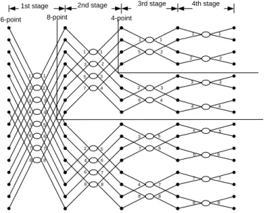
The conventional butterfly order starts from top to down and from left stage to right stage of the FFT signal flow graph, as shown with the numbers marked on the right side of ellipses in Fig. 1. On the other hand, the main idea of Cohen’s processing order is grouping butterflies with the same coefficient together to reduce switching activities of the coefficient generation circuits. Then the processing order is changed as the numbers marked on the left side of ellipses in Fig. 1.
1 2 3 4 5 6 7 8 1 2 3 4 5 6 7 8 1 3 5 7 2 4 6 8 1 2 3 4 5 6 7 8 1 5 2 6 3 7 4 8 1 2 3 4 5 6 7 8 1 2 3 4 5 6 7 8 8 7 6 5 4 3 2 1 16-point 8-point 4-point
1st stage 2nd stage 3rd stage 4th stage
Fig. 1. Different butterfly processing sequence between fixed-length and variable-length memory based FFT processors.
In order to generalize the control schemes in different OFDM operation modes, operation of shorter-length mode is identical to a segment of operation of a longer one. In Fig 1, however, we can find out that Cohen’s scheme is not suitable for a variable-length FFT as can be realized when we isolate a segment of signal flow graph for a shorter-length FFT. In order to have a variable-length FFT design, we propose the following data address generator.
The data address generation function that causes top-to-down processing order is driven by butterfly counter per stage and stage counter. Total butterfly count of
radix-2 DIF FFT is
2 log2N
N
, and the number of bit of total butterfly counter is
1 ) log (
counter and the remaining lower bits are butterfly counter per stage.
The ith butterfly pair of the kth stage is represented by <s, t> and the relationship
between s, t, and i, k are
) 2 mod( 2 2 * )) 2 mod( ( ) 2 mod( 2 * )) 2 mod( ( 1 1 1 1 1 k k k k k i i i t i i i s (1)
The algorithm is equivalent to a binary insertion operation of the counter value
} , , ,... , {ilog( ) 2 ilog( ) 3 i2 i1 i0 i N N (i.e.,
log( ) 2 0 2 * N j j j ii ) as described by the following
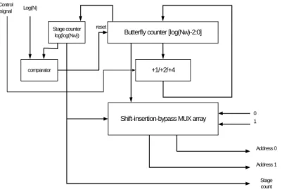
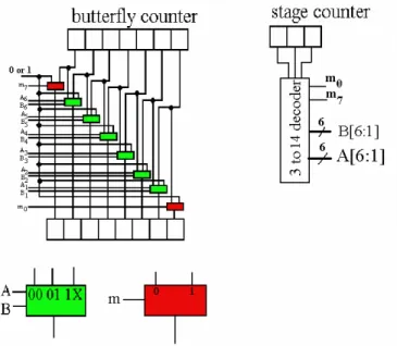
equation, } , ,..., , , 1 , ,..., , { } , ,..., , , 0 , ,..., , { 0 1 3 2 1 3 ) log( 2 ) log( 0 1 3 2 1 3 ) log( 2 ) log( i i i i i i i t i i i i i i i s k k k N N k k k N N (2) We can use multiplexer to shift some bits left, then insert zero or one, and bypass the remaining bits to realize the data address generation algorithm. The data address generator and detail architecture of shift-bypass-insertion multiplexer array are shown in Fig. 2 and Fig. 3, respectively.
Stage counter
log(log(Nw)) Butterfly counter [log(Nw)-2:0]
+1/+2/+4
Shift-insertion-bypass MUX array
comparator reset Log(N) Control signal 0 1 Address 0 Address 1 Stage count
Fig. 3. Architecture and operation of shift-insertion-bypass multiplexer array.
Each bit of s or t excluding MSB and LSB has three possible inputs: the bit of the same index of butterfly counter, the bit of the previous index of butterfly counter, and the insertion bit (zero or one).
The external control unit should provide two signals for counter, one is for butterfly counter to decide count step size to implement variable-length application, another is for stage counter to decide when to reset the counter. The stage counter and butterfly counter are designed to adopt the longest FFT length. To change the
maximum counting number from N/2 to N/2c+1 of a butterfly counter, we can realize it
by controlling the count step from 1 to 2c. Another control signal is the termination number to be compared with the count of a stage counter. If a stage counter reach the termination number, all counters are reset to zero and start to process the next N-point data.
2.2 A New Coefficient Index Generator
2.2.1 Fixed-Radix DesignCoefficient address generation is also driven by stage counter and butterfly counter. The translation between counter contents of data address generator and coefficient address is dependent on the FFT algorithm. The major difference between coefficient address generators of a fixed-length FFT processor and a variable-length one is the coefficient selection order. Fixed-length FFT processor, in Cohen’s scheme, accesses the coefficient once then process all the butterflies corresponding to the same
coefficient to reduce transition and power consumption of the coefficient related circuits. However, due to its limitation in the variable-length design, this execution schedule is not efficient as mentioned in previous section. Based on this butterfly operation sequence, a direct and simplified coefficient address generating algorithm is proposed for variable-length FFT processor as detailed below.
Coefficients of a shorter size FFT are subset of a longer one, and coefficients of latter stages are the subset of former ones in the fixed-radix FFT data flow. Already known that the basic coefficient address generating function is a counter. And by changing the counter steps, one can access coefficients for FFT with varying stages and variable lengths.
In fixed-radix design, there are two schemes to generate different step of coefficient address. One is shifting the content of butterfly counter to left by barrel shifter, and appending zeros to the emptied LSB’s, as shown in Fig. 4, where the shift amount is dependent on the stage counter.
Stage
Counter Butterfly Counter
+
Barrel Shifter M U X carry+
Mode_control 0 2 3 M U X 1 4 8 Shift amount Coefficient addressFig. 4. Fixed-radix, variable-length coefficient index generator, scheme A. Another way is importing a coefficient counter content whose counter step corresponds to the FFT size (as the butterfly counter) and stage counter. The coefficient counter doubles its counter step when the stage counter increase its count by one, then the counter and butterfly counter are reset simultaneously. Realization of this solution is shown in Fig. 5.
Stage
Counter Butterfly Counter
+
Barrel Shifter carry Mode_control M U X 1 4 8 Coefficient address Coefficient Register S h if t a m o u n tFig. 5. Fixed-radix, variable-length coefficient index generator scheme B.
2.2.2 Split-Radix Design
It is difficult to design coefficient address generator for split-radix FFT, due to irregular data flow of the split-radix algorithms. One solution is to append a flag bit in data memory to record the coefficient access states.
Coefficient usage states for the split-radix 2/4 FFT algorithm can be classified as two modes: mode 0 indicates that all data are in initial state or the data are from addition results of the butterfly processes in the previous stage, while mode 1 indicates that the data are from the subtraction results of the butterfly processes in the previous stage, as shown in Fig. 6. These two modes reflect different behaviors in coefficient access. By appending a mode flag bit to the processed data, one can on-line indicate the operation states easily, otherwise one needs to design a complicated control circuit for this function.
+
+
+ + + -Addition port Subtraction port Input ports Mode 0 Mode 1Fig. 6. Mode assignment of butterfly PE in SR-2/4 FFT
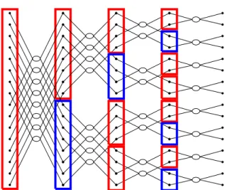
In the data flow graph shown of Fig. 7, red and blue marks represent Mode 0 and Mode 1, respectively, of the data states. When the controller detects that the coefficient access is in Mode 0, then the output data from addition result in the current butterfly is flagged as Mode 0, while and the output data from subtraction result is flagged as Mode 1. When the controller detects that the coefficient is in Mode 1, then all output data from the current butterfly are marked as Mode 0.
Fig. 7. Mode assignment in 16-point SR-2/4 FFT data flow graph. When controller detects that the input data are Mode 0, the first N/2k output data from the addition results, and output data from subtraction results are bypassed without multiplication, where N and k are FFT length and stage number, respectively. The remaining N/2k output data from
subtraction ports are multiplied by –j, which is simply swapping real and
imaginary parts then negating imaginary part of the operand. If controller detect that the input data are in Mode 1, the output data from addition
results are multiplied by coefficients from 0
2 / k2 N W to ( /2 ) 1 2 / 2 k k N N W , and the
output data from subtraction results are multiplied by coefficients from
0 2 / k2 N W to 3( /2 ) 3 2 / 2 k k N N
W . The architecture of variable-length coefficient
generator for split-radix 2/4 is shown in Fig. 8.
Stage
Counter Butterfly Counter
+ Barrel Shifter M U X carry + Mode_control 0 2 3 M U X 1 4 8 Shift amount Coefficient Address_A Previous stage x 3 Coefficient Address_B
Fig. 8. Architecture of variable-length coefficient index generator for SR-2/4 FFT.
regardless of data modes, and external mode selector will control the usage of coefficients. There are a few differences between radix-2 coefficient generator and split-radix 2/4 one. One is that the coefficient base for each stage of the split-radix 2/4 version is equal to the previous stage of the radix-2 version. Hence, a register is used to record the previous stage and control the shift amount of barrel shifter. Another difference is that a fixed coefficient multiplier is used to generate a 3X index of coefficient address for the subtraction output. This hardware simultaneously generates two coefficient addresses for the addition and subtraction results each cycle. However, not all of them are applied to all the operations, because the mode selector may switch to bypass or swap-and-invert modes for special coefficients multiplications as mentioned before.
2.3 A New Coefficient Generator
In FFT PE design, coefficients are conventionally realized by a look-up table (LUT), which costs a large chip area to realize long-length FFT. For example, considering a 16-bit accuracy 8192-point FFT (required by DVB-T and VDSL), and utilizing the
symmetry property of coefficients, it needs 32768( ) 4( )
8 1 8192 16
2 bit KB
size of LUT. In the following we propose a simple algorithm that can be implemented with low cost that can replace LUT to save chip area.
The sine and cosine function generation equations are shown in equations (3) and (4), respectively. ) 2 sin( ) 1 sin( cos 2 ) 2 sin( } sin ) 2 cos( cos ) 2 {sin( cos 2 sin cos ) 2 cos( 2 ) 2 sin( cos ) 2 sin( 2 sin cos ) 2 cos( 2 ) 1 cos 2 ( ) 2 sin( sin cos ) 2 cos( 2 ) sin (cos ) 2 sin( sin ) 2 sin( sin cos ) 2 cos( cos sin ) 2 cos( cos ) 2 sin( sin } sin ) 2 sin( cos ) 2 {cos( cos } sin ) 2 cos( cos ) 2 {sin( sin ) 1 cos( cos ) 1 sin( ) sin( 2 2 2 2 2 2 n n n n n n n n n n n n n n n n n n n n n n n (3)
) 2 cos( ) 1 cos( cos 2 ) 2 cos( } sin ) 2 sin( cos ) 2 {cos( cos 2 ) 2 cos( sin cos ) 2 sin( 2 cos ) 2 cos( 2 sin cos ) 2 sin( 2 } 1 cos 2 { ) 2 cos( sin cos ) 2 sin( 2 } sin {cos ) 2 cos( sin ) 2 cos( sin cos ) 2 sin( cos sin ) 2 sin( cos ) 2 cos( sin } sin ) 2 cos( cos ) 2 {sin( cos } sin ) 2 sin( cos ) 2 {cos( sin ) 1 sin( cos ) 1 cos( ) cos( 2 2 2 2 2 2 n n n n n n n n n n n n n n n n n n n n n n n (4) Both sin and cosine function are generated from the recursive equation Y(n)=2cos*Y((n-1))-Y((n-2)) so that twiddle factors of sequential angle can be generated from the sine and cosine of initial angle through this recursive equation.
Because of the finite accuracy of data, error will propagate with the angle accumulation. One solution is using small LUT to correct each LSB of output to prevent error propagation to the next iteration. The quantization error analysis of this algorithm is shown in equation (5).
) 1 2 ( 1 ) 1 ( ) 1 2 ( ) 1 ( ) 1 ( ) 1 ( 2 ) 2 cos ) 1 sin( ( 2 ) ) 2 sin( ) 1 sin( cos 2 ( 2 ) 2 sin( 2 cos 2 ) 1 sin( 2 ) 1 sin( cos 2 ) 2 ) 2 sin( ( ) 2 ) 1 sin( ( ) 2 cos ( 2 sin n n n n n n n n n m m m m m m m m m (5) Therefore maximum error of each iteration is
) 2 ( ) 1 2 ( 1 2 2 ) 2 cos ) 1 sin( ( 2n m n n (6) According to equation (6), we need a 2-bit compensation LSB’s for each initial angle. The compensation bits are stored in a LUT. The correction bits are retrieved to replace LSB’s of each output coefficient from the coefficient generator. Architecture of the proposed coefficient generator is shown in Fig. 9.
Y(n-1) Y(n-2) X + MUX MUX In itia l c o s in e Select + -0 M U X Replace LSB C o rr e c t L U T Counter Select In itia l s in e (a) Y(n-1) Y(n-2) X + MUX MUX In itia l c o s in e Select + -1 M U X Replace LSB C o rr e c t L U T Counter Select (b) Fig. 9. (a) Architecture of coefficient generator for sine function.
(b) Architecture of coefficient generator for cosine function.
The coefficient generator is designed for 8192, 4096, 2048, 1024, 512, 256, and 64 point FFT’s. In total we need a 14-words LUT (7 for initial sine and 7 for initial cosine) for the initial angle values, and 2048 bits of correct LUT, plus 2 adders, 2 multipliers, and 4 word registers.
2.4 The Proposed FFT Processor Architecture
Control signals, including memory read and write address, PE state, and coefficient indices, are generated automatically in our FFT processor design example. There are four operation states of our FFT processor so that the controller generates four types of control signals with a stationary sequence as shown in Fig. 10.
IDLE WRITE FFT READ WRITE FFT . . . . .
Fig. 10. States change sequence of FFT processor.
State IDLE is asserted when system reset, data is loaded from the front end of the system to main memory during state WRITE, data is unloaded from the main memory to the back end of the system during state READ, and all butterfly operations of one N-point frame are executed in the state FFT. After state IDLE, controller continuously generates control signals following the fixed WRITE-FFT-READ sequence.
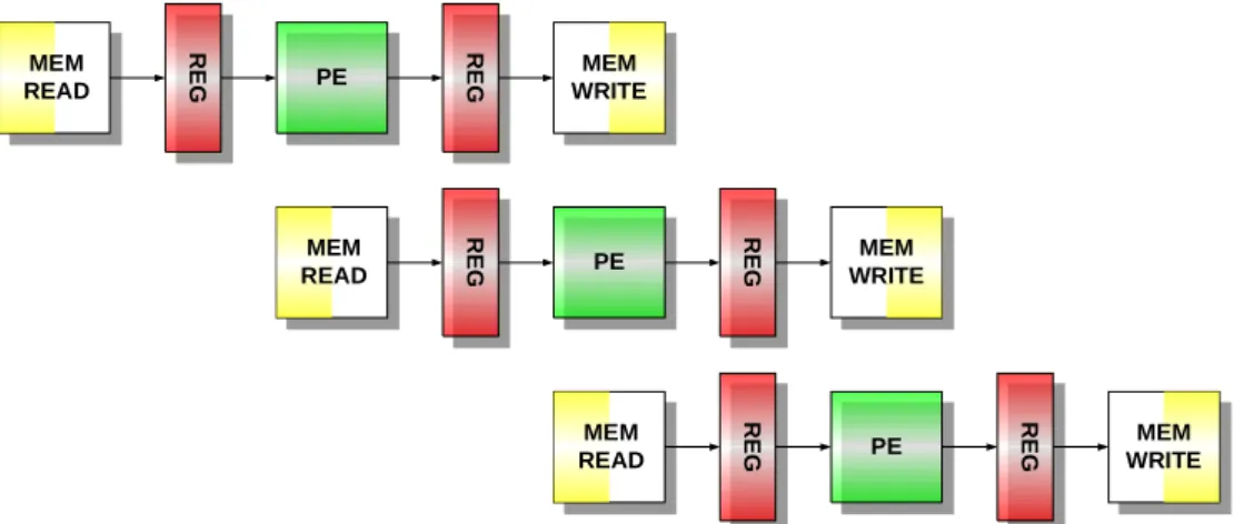
Inside the FFT processor, operation can be divided into three major parts: memory read, data processing, and memory write back. These three parts are isolated by two sets of register so that they can operate simultaneously and independently without conflict. The FFT operation diagram of our design example is shown in Fig. 11.
PE R E G R E G MEM READ MEM WRITE PE R E G R E G MEM READ MEM WRITE PE R E G R E G MEM READ MEM WRITE
Fig. 11. Pipelined data path and shared devices of FFT processor.
The diagram shown in Fig. 11 is normal butterfly operation that data load and unload between FFT processor and external system are not considered and detail description of data load and unload will presented latter.
According to the pipelining behavior, control signal that is generated at initial of each butterfly process should be held in registers to control latter pipeline stage. In normal butterfly process, memory read address is direct extracted from counters without holding in registers and PE control signal and memory write back address should be held in registers one and two cycle, respectively. Data loading has different behavior from memory writing of normal butterfly processing because the data loading need not to delay two cycle to wait for ready output data from PE. The memory writing behavior is both controlled by immediate and delayed two cycle control signal according to the state of FFT processor. Fortunately, these control signals would not conflict in continuous FFT processing as shown in Fig. 12.
Write_Enable Write_Address Write_Address Delayed_2 WRITE WRITE WRITE WRITE READ READ FFT FFT FFT FFT
Fig 12. Memory write control behavior. Different segments of address bus stand for address generated in different states and red marks stand for selected address for memory write.
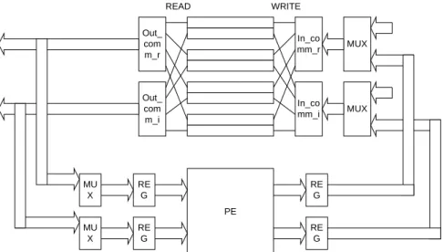
In our radix-22 algorithm based design example, data load and unload path and
commutators beside read port and write port of memory should be considered. The whole data path is shown in Fig. 13.
Out_ com m_r Out_ com m_i In_co mm_r In_co mm_i PE READ WRITE MUX MUX RE G RE G MU X MU X RE G RE G
Fig. 13. Data path of Radix-22 based VL-FFT processor.
The MUXs before input register of PE apply to switch input of PE between zero and memory output data. During state IDLE, READ, and WRITE, there is no valid operation of PE and set input of PE stationary like equal to zero can lower power consumption of PE. Block out_comm_r and out_comm_i stand for output commutator of real part and imaginary part data respectively that commutate data from four memory banks to correct PE input ports according to commutation control signal extracted from data address. Block in_comm_r and in_comm_i stand for input commutator of real part and imaginary part data, respectively. These two block commutate output data of PE to correct memory banks that the mapping relationship are inverse of block out_comm_r and out_comm_i to write data back to original memory bank. Another set of MUXs site before input commutators apply to switch memory write data between loading data from front end of system and write back data from output ports of PE according to FFT processor state.
Because of the registers inserted between memory and PE, memory access and PE operation can work simultaneously.
2.5 A New Channel Estimation Algorithm Based on DCT
Orthogonal frequency division multiplexing (OFDM) is a highly efficient and popular technique for high bit-rate data transmission over wireless communication channels. It has been adopted in wireless LAN and MAN standards IEEE 802.11a and 802.16, and the European digital audio broadcasting (DAB) and digital video broadcasting (DVB) standards.
In wireless communication channels, multi-path is a very common and severe problem. It causes inter-symbol interference (ISI) in the signal stream and this may degrade the transmission efficiency. OFDM can easily
avoid this problem by inserting guard interval (GI). Besides ISI, multi-path also causes frequency-selective fading. If coherent demodulation is adopted, the effect of amplitude and phase fluctuation should be mitigated. One typical solution is to perform channel estimation, followed by channel equalization. Generally, there are two types of approaches for channel estimation. One is blind type of algorithms [7] and the other is pilot-aided type of algorithms [8]. Although the pilot-aided algorithms waste a little more bandwidth than the blind algorithms, their performance is usually better than that of the blind case. Pilot-aided approach has been adopted in many standards such as 802.11a and many others. Therefore, in this paper we will focus on the pilot-aided case.
The optimal interpolation filtering in Minimum Mean Square Error (MMSE)
sense for channel estimation [9], [10] needs the information of channel
statistic and the associated computation complexity is very high. This may be hard to implement in practice. The approach of DFT-based interpolation [11] can theoretically achieve ideal lowpass interpolation, and has the advantages of low complexity by employing FFT algorithms. This technique works well when multi-path delays are integer multiples of the sampling time. However, this hardly happens in practical transmission environment. When the condition is not satisfied, performance of the DFT-based algorithm may degrade considerably. This is because the equivalent channel impulse response will be a disperse version of the original shorter one [12]. As a result, the DFT-based interpolation process will be based on the aliased data of the disperse impulse response.
In this paper, for the consideration of better channel interpolation result and lower aliasing error, we will propose a DCT-based channel estimation method, as detailed below.
2.5.1 Channel Estimation Based on DFT Interpolation 2.5.1.1 OFDM SYSTEM MODEL
We assume that an OFDM symbol contains N sub-carriers, and the OFDM symbol duration is T. Then the sampling time will be T/N and the sub-carrier spacing is 1/T. The transmitted signal can be expressed as:
(t) θ D t s i N n i,n i,n
1 0 ) ( (7)where Di,n is the data on the n-th sub-carrier in the i-th OFDM symbol and ( ) ( )[ ( ) ( ( 1) )] π 2 , c c iT T t T n j n i t e u t iT u t i T c g (8)
where Tg is the guard time interval and Tc= Tg + T is the total symbol duration. u(t) is
the step function.
A multi-path channel can be characterized as:
) ( ) ( ) , ( 1 0 i L i i t t h
(9)where i(t) is the time-varying gain and is the delay time for the i-th path. L is i
the total number of the paths. Usually, i(t) is modeled Rayleigh distributed, and the
variation is associated with Doppler frequencyfd, fd fcv/c wherefc is the carrier frequency, v is the vehicle speed and c is the velocity of light.
The received OFDM signal passing through the AWGN time-varying multi-path channel can be expressed as
) ( ) ( ) ( ) ( 1 0 t n t s t t r i L i i
(10)where n(t) is the white Gaussian noise. After sampling the signal and removing guard
interval, the equivalent channel frequency response is (assuming i(t) is constant
over one OFDM symbol)
1 0 2 , , L i T k j i s k s i e H (11)whereHs,kis channel frequency response corresponding to the k-th sub-carrier of the
s-th symbols, and s,i is the gain of the i-th path during the s-th symbol period. The
received signal on the k-th sub-carrier of the s-th symbol can be expressed as
k s k s k s k s D H N Y, , , , (12)
The corresponding impulse response is [12]
1 1 ) ) 1 ( ( , , ) / ) ( sin( ) sin( 1 L i i i N N n j i s n s N n e N h i (13)where hs,n is the n-th tap of channel impulse response during the s-th symbol and
i
=i/Ts, where Ts is the sampling time. By this equation, when non-integeriexists,
the power will leak to all taps hs,n, as shown in Fig. 14.
2.5.1.2 DFT-BASED CHANNEL ESTIMATION [13]
Assume that M pilots are evenly assigned to M sub-carriers out of total
N sub-carriers at a spacing of N/M sub-carriers, where N/M is an integer.
The DFT-based channel estimation algorithm begins with the least square (LS) estimation of the pilot sub-carriers.
0 5 10 15 0 0.2 0.4 0.6 0.8 1 1.2 1.4 n h ( n )
Fig. 14. The equivalent impulse response for the continuous channel
) 4 . 1 ( ) 5 . 0 ( ) ( ) (t t t Ts t Ts h m m p m p Y p H , , / (14)
where Yp,m is the received signal at the m-th pilot sub-carrier and pmis
the pre-assigned pilot value for the m-th pilot. Then Hp,m
is multiplied by some linear-phase shift as shown below
MT m jπ p,m p',m H e H (15) whereβ is the minimum integer greater than all the path delays. The
operation amounts to a corresponding time shift of the impulse response. It would make the power of the impulse response much more concentrate
around t=0, while the impulse response values in the middle time positions
would be smaller. This will facilitate zero insertion in those positions, and lead to a more effective up-sampling result of the channel frequency response, than the case without phase adjustment, as detailed below.
First the M-point impulse response is obtained by
} { } {hp IFFT Hp' (16)
Next the zero-insertion impulse response is formed by inserting (N-M)
zeros in the middle time indices:
otherwise h M N n M M n h h M N n p n p n N , , , 0 /2 /2 1 1 2 / (17)
Then the interpolated channel frequency response is solved after performing FFT on
N h . } { } {Hsh FFT hN (18)
Finally, the actual estimated channel frequency response is obtained by canceling the phase shift operations performed in the beginning stage of the algorithm:
NT n jπ sh,n n H e H (19)
2.5.2 The Proposed Algorithm
As mentioned before, there will be leakage in channel impulse response, when the path delays are non-integer multiples of the sampling time. It is obvious that DFT-based interpolation is not suitable for channel estimation under this condition. This is because the leakage will cause severe aliasing, when the mentioned DFT-based method is used. [13] proposed a windowed DFT-based approach to improve the performance. However, this approach must sacrifice some bandwidth. Next, we will propose a DCT-based interpolation algorithm to mitigate the aliasing problem. DCT is a well-known technique extensively used in image processing. DCT can reduce the high frequency component in the transform domain compared with DFT. The reason is that when given a sequence of N-point data, DFT conceptually treats it as a periodic signal with a period
of N points. Hence, there is a tendency of noticeable high-frequency
components, due to signal discontinuity in between consecutive period
boundary. In contrast, DCT conceptually extends the original N-point data
sequence to 2N-point sequence by doing mirror-duplication of the N-point
data sequence. As a result, the waveform will be smoother and more continuous in the boundary between consecutive periods. Correspondingly, high frequency components will be reduced. This benefits interpolation process. The proposed DCT-based channel estimation algorithm is detailed below:
2.5.2.1 THE NEW DCT-BASED CHANNEL ESTIMATION ALGORITHM
First, we also use LS estimation to get the channel frequency response on the pilot sub-carriers. After that, we perform DCT
0 , 2 ; 0 , 1 1 0 , 2 ) 1 2 ( cos 1 0 , ,
k M w k M w M k M k m H w h k k M m m p k k c (20)The next step inserts zeros in the DCT domain. However, different from DFT-based
interpolation, zeros must be inserted at the end of hc
as
otherwise M k h h ck k N 0 1 , , k0 N1 (21)
Here IDCT can’t be directly performed on hN
to get the channel frequency response
due to the following reason. Compared with DFT, DCT has a shift in the time domain data. After zero-insertion in the DCT domain, the corresponding shift amount will change. The shift cannot be recovered by N-point IDCT. The solution is to use extendible IDCT (EIDCT) [14]. Based on EIDCT, we can get the interpolated channel estimation as 1 0 ) ) 1 cos(( 1 0 ,
N n k M N n h w H M k k N k n (22)Alternatively, since the transform is derived from the concept of DFT, we can get the same result by first doing mirror-duplication to get doubled-length data and then applying the DFT-based interpolation.
One may argue that we can exchange the DCT and IDCT process in the interpolation, then the time shift problem will not occur. Indeed, this is true. However, if we adopt this approach, another problem similar to DFT-based interpolation will be introduced. In the M-point DCT transform (20), its value is always zero at k=M. Therefore, if we treat the original data as DCT transform domain signal, the estimated channel frequency response after interpolation will decay to zero outside the last pilot sub-carrier. As it turns out, this would lead to degradation of performance at the edge of spectrum.
2.5.2.2 COMBINING A NOISE REDUCTION SCHEME
When the delay time of each path is close to zero, the white Gaussian noise can be effectively reduced in the DCT domain. If the path delays are all small, the channel frequency response will be smoother (with less high frequency components). As such, in the DCT domain, the power in the high frequency region can be viewed as noise, and we can eliminate it by setting the value of high frequency to zero. The method works better in the DCT domain than in the DFT domain [11]. Especially, this is most effective when the pilot power is not much lager than the noise power. When the pilot power is limited to a lower level, for low-power consideration, this method can improve performance. The whole operations are detailed below.
After DCT operations, the accumulated power counting from the first index can be calculated. The value is compared with a threshold to determine the region occupied mostly by noises. One way to define the threshold is using percentage of total power, e.g. 90% of total power. After the index is determined, all the impulse response values after this index are set to zero as
1 0 0 , , M k b b k h h ck k cc (23)
where b is the index of threshold
Note that whether DCT-based or DFT-based approach, the delay spread must
be smaller than (M.Ts). Otherwise, the estimation will be error prone.
This can be explained by the concept of down sampling. The frequency responses at the pilot sub-carrier frequencies are the down sampling
version of the complete channel frequency response at all N sub-carrier
frequencies. Hence, if the delay spread is equal to or lager than (M.
Ts), then the aliasing of channel impulse will occur. There is no way to
recover the aliased impulse response.
0 5 10 15 20 25 30 35 40 45 10-3 10-2 10-1 100 SNR S y mbol err or rat e DCT-based estimator DFT-based estimator
Fig. 15. The SER performance with DCT-based estimator compared with DFT-based estimator
2.5.4 Simulation Results
In this section, we present the simulation result of the DCT-based estimator and compared it with DFT-based approach. The multi-path Rayleigh fading channel is simulated by Jakes’ model. And each path gain follows the exponential power delay profile. i e t E i ] ) ( [ 2 (24)
We assume the channel has 4 paths and the set of delay spread is {0, 3.5Ts, 7.3Ts, 10.4Ts}. Meanwhile, we choose μ such that the average power of last path will be 20dB less than first path.
The number of total sub-carriers is 1024. 32 pilots are evenly inserted into the sub-carriers, and the first pilot is put on the first sub-carrier. Assume the transmission bandwidth is 5MHz. Then the sub-carrier spacing is 4.883KHz, and the sampling
period is 0.2 . The Doppler spread is fixed at 50Hz, such that s fdT0.01. The
modulation scheme on each sub-carrier is 16QAM. The guard time interval is 32 sample periods. As for the value assigned to pilot, the outmost constellation point in 16QAM is chosen. Fig. 15 shows the simulation result. It is obvious that DCT-based approach noticeably has higher performance especially in high SNR, than the DFT counter part.
We also simulate the case when the proposed new algorithm method combines with a noise reduction scheme as mentioned before. In this case, the set of delay spread is assumed {0, 0.5Ts, 2.2Ts, 3.1Ts}. As explained previously, the delay values cannot be too far away from zero. Also we change the pilot value from the outmost constellation point in 16QAM to the innermost point to reduce the pilot power. The threshold is set to 90% of the total power. Fig. 17 depicts the simulation result.
0 5 10 15 20 25 30 35 40 45 10-3 10-2 10 -1 10 0 SNR Sy mbol err or rat e DCT-based estimator
DCT-based estimator with noise reduction
Fig. 17. The SER performance of DCT-based estimator with noise reduction
A DCT-based pilot-aided channel estimator of OFDM system in the multi-path fading channel with non-integer sample-spaced path delay has been proposed in this paper. It achieves significant improvement over the DFT-based approach. It can be realized by the mature, low-complexity fast DCT algorithms in the literature. It is much lower than many other well-known matrix-based estimators. For the case of small path delay spreads and pilots with low power level, we also propose an effective noise reduction method to improve the performance.
3. Conclusion
In the midterm report, we describe five preliminary results. In summary, the current results already exceed the expected results. Besides the ongoing project are going smoothly on tract as planned. For this year’s project, we already published too papers on ISCAS’03 and ICASP03, respectively, one is on FFT design and the other is on OFDM channel estimation
References
[1] J. W. Cooley and J. W. Tukey, “An Algorithm for Machine Computation of Complex Fourier Series,” Math. Computation, Vol. 19, pp. 297-301, April 1965. [2] D. Cohen, “Simplified Control of FFT Hardware,” IEEE Trans. Acoust., Speech
Signal Processing, Vol. ASSP-24, pp. 577-579, Dec. 1976.
[3] L. G. Johnson, “Conflict Free Memory Addressing for Dedicated FFT
Hardware,” IEEE Transactions on Circuit and System-II: Analog and Digital
Signal Processing, Vol. 39 No.5, pp.312-316, May 1992.
[4] Hsin-Fu Lo, Ming-Der Shieh, and Chien-Ming Wu, “Design of an Efficient FFT
Processor for DAB System,” IEEE International Symposium on Circuits and
Systems, Vol. 4, pp. 654 –657, 2001.
[5] Yutai Ma, “An Effective Memory Addressing Scheme for FFT Processors,”
IEEE Transactions on Signal Processing, Vol. 47 Issue: 3, pp. 907-911, March
1999.
[6] Yutai Ma and Lars Wanhammar, “A Hardware Efficient Control of Memory Addressing for High-Performance FFT Processors,” IEEE Transactions on Signal Processing, Vol. 48 Issue: 3, pp. 917-921, March 2000.
[7] H. Bolcskei, R. W. Heath, Jr., and A. J. Paulraj, “Blind Channel Identification and Equalization in OFDM-Based Multiantenna Systems,” IEEE Trans. Signal Processing, vol. 50, no. 1 January 2002, pp. 96-108.
[8] Y. Li “Pilot-symbol-aided channel estimation for OFDM in wireless systems,“ IEEE Trans. Veh. Technol., vol. 40, no. 4, pp.1207-1215, July 2000. [9] Y. Li, L. J. Cimini, Jr., and N. R. Sollenberger, “Robust channel estimation for
OFDM systems with rapid dispersive fading channels,” IEEE Trans. Commun., vol. 46, no. 7, pp. 902-915, July 1998.
[10] O. Ddfors, M. Sandell, J. J. van der Beek, S. K. Wilson, and P. O. Borgesson, “OFDM channel estimation by singular value decomposition,” IEEE Trans.
Commun., vol 46, no. 7, pp. 931-939, July 1998.
[11] Y. Zhao and A. Huang, “A Novel Channel Estimation Method for OFDM Mobile Communication Systems Based on Pilot Signals and Transform-Domain Processing,” Proc. VTC’97, pp. 2089-2094.
[12] J.J. van der Beek, O. Edfors, M. Sandell, S.K. Wilson, and P. O. Borgesson, “On Channel estimation in OFDM systems,” Proc. VTC’95, pp. 815-819.
Pilot-symbol-Aided Channel Estimation for OFDM Systems in Multipath Fading Channels,” Proc. VTC’00-Spring, vol. 2, pp.1480-1484.
[14] Y. F. Hsu, Y. C. Chen, “Rational interpolation by extendible inverse discrete cosine transform,” Electronics Letters, vol. 33, no. 21, 9 Oct. 1997, pp. 1774-1775.