新型低溫複晶矽非揮發性奈米鍺晶體捕獲儲存層記憶體元件
86
0
0
全文
(2) 新型低溫複晶矽非揮發性奈米鍺晶體捕獲儲存層 記憶體元件 Novel Low Temperature Poly-Si Thin Film Nonvolatile Memory with Ge nanocrystals Trapping Layer. 研究生 :黃竣祥 指導教授:趙天生 博士. Student:Jyun-Siang Hunag Advisor:Tien-Sheng Chao. 國 立 交 通 大 學 電子物理學系 碩士論文. A Thesis Submitted to Department of Electrophysics National Chiao Tung University In partial Fulfillment of the Requirements For the Degree of Master of Science In Electrophysics June 2006 HsinChu, Taiwan, Republic of China. 中華民國 九十五年 六月.
(3) 新型低溫複晶矽非揮發性奈米鍺晶體捕獲儲存層 記憶體元件 研究生:黃竣祥. 指導教授:趙天生 博士 國立交通大學 電子物理學系 摘要. 在本論文中,我們提出在低溫複晶矽薄膜上製作非揮發性快閃記憶體元件。為了克 服傳統浮動閘極記憶體結構微縮的瓶頸,已有奈米矽晶體記憶體元件被提出。當穿隧介 電質變薄時,奈米晶體記憶體被證實有良好的資料保存特性以及較低的電源損耗。由於 鍺相較於矽有較小的能帶間隙以及較低的結晶溫度,並且相容於目前的 CMOS 製程技術, 我們首次提出並成功地製作低溫複晶矽非揮發性奈米鍺晶體膜薄記憶體元件。由穿透式 電子顯微鏡可知奈米鍺晶體直徑大約為 10 奈米,且元件的記憶體特性以及其可靠度也 相當穩健。我們亦利用薄膜電晶體元件的基本特性,提出利用浮接基體引發汲極雪崩熱 電子之寫入操作模式,並進一步探討此寫入模式在不同通道薄膜厚度以及不同元件尺寸 所造成的寫入效益特性以及其所需之操作電壓。在寫入速度的特性量測中,我們發現因 通道薄膜厚度越薄、元件尺寸越小時,會有越顯著的浮接基體效應,所以以較低的操作 電壓(10 伏特)即可有很快的寫入速度,10 微秒即可達到約 1 伏特的記憶視窗。此一現 象表示浮接基體引發汲極雪崩熱電子有極高的注入效益。在另一方面,我們使用能階對 能階熱電洞注入作為抹除操作模式,亦探討在不同通道薄膜厚度和不同元件尺寸之抹除 速度以及其所需之操作電壓。在抹除速度的特性量測中,我們發現元件尺寸越小,可以 較低的操作電壓(10 伏特)即可達到很快的抹除速度,抹除時間亦在微秒等級。 在非揮發性記憶體元件中,最重要的兩項可靠度問題為資料保存能力以及寫入抹除 耐久度測試。我們亦針對此兩項可靠度問題對我們的元件進行測試。我們分別在室溫以 及 85oC 高溫進行資料保存能力測試。在室溫方面,奈米鍺晶體表現出優異的資料儲存能 o. 力,推測十年後的電荷保存能力可維持在 90%以上。但在 85 C 高溫,由於穿隧氧化層之 品質較差所以導致部份儲存電荷流失。在另一寫入抹除耐久度測試方面,記憶體元件經 過資料反覆寫入及抹除一萬次,記憶視窗都可維持在 60%以上,並無因為反覆寫入抹除 I.
(4) 而造成記憶視窗關閉的情形。由於快閃記憶體設計皆為元件陣列排列,故抗閘極干擾以 及抗汲極干擾亦是相當重要的問題。我們也分別對抗閘極干擾以及抗汲極干擾特性進行 研究,實驗觀察中發現我們的元件有優良的抗閘極干擾,經由 1000 秒的閘極電壓應力 測試,臨界電壓漂移皆可控制在 0.3 伏特以內。在抗汲極干擾方面,由於汲極電壓應力 造成穿隧氧化層內載子捕獲態的產生,使得臨界電壓往上漂移。但經 100 秒測試,臨界 電壓漂移亦在 0.4 伏特以內。由於我們製作的載子捕獲層為分離之奈米鍺晶體,所以我 們進行單一記憶胞多重位元之操作特性研究。經由一次的寫入動作之後,利用不同正向 汲極電壓進行讀取,即可讀取到不同的臨界電壓值。由此特性研究,亦同時證實我們的 載子捕獲層確實為分離之奈米鍺晶體並且單一記憶胞具有多重位元儲存之能力。從我們 的研究可知,低溫複晶矽非揮發性奈米鍺晶體膜薄記憶體元件具有相當優異的寫入抹除 速度以及元件越微縮亦以較小操作電壓及達到快速操作速度,並且具有單一記憶胞多重 位元儲存之能力。若能增進穿隧氧電層之品質以大幅改善元件之可靠度,相信未來在低 溫複晶矽非揮發性記憶體元件的應用將有優異的表現。. II.
(5) Novel Low Temperature Poly-Si Thin Film Nonvolatile Memory with Ge nanocrystals Trapping Layer Student:Jyun-Siang Huang. Advisors:Dr. Tien-Sheng Chao. Department of Electrophysics National Chiao Tung University. Abstract In this thesis, we proposed the fabrication of low temperature polycrystalline silicon thin film with nonvolatile flash memory as named the SONOS-type poly-Si TFTs memories. To overcome the scaling limits of the conventional FG structure, Tiwari et al. for the first time demonstrated the Si nanocrystal floating gate memory device in the early nineties. Also, the nanocrystal memory device can maintain good retention characteristics when tunnel oxide is thinner and lower the power consumption. Due to the relatively small band-gap compared to Si and compatibility with CMOS technology currently used, germanium nanocrystal is considered to be an idea memory node. We, for the first time, demonstrated Ge nanocrystals for low temperature poly-Si TFTs memory device application. We utilized the basic characteristic of thin film devices, and proposed floating body induced drain avalanche hot electrons injection for program operation mode. And further, we investigated the injection efficiency and operations voltage on different channel thickness and size device for this program mode. For program speed measurement, we found serious floating body effect for thicker channel thickness and smaller size device. Accordingly, it needed only lower drain voltage bias and then can reach faster program speed. This phenomenon revealed that injection efficiency of floating body induced drain avalanche hot electrons is very high. On the other hand, the erase operation mode is band-to-band hot holes injection. And for program speed measurement, we also found that it needed only lower drain voltage bias and then can reach faster erase speed. The program and erase of our device needs time smaller than ms order. We also discussed two important reliability issues. They are data retention and P/E cycle called endurance, respectively. We measured the data retention at room temperature and high temperature at 85oC. At room temperature, Ge nanocrystals show excellent capability of. III.
(6) data retention. But at 85oC, bad tunnel oxide quality resulted in charge loss. For endurance, memory window can maintain above 60% after 104 P/E cycle without threshold voltage window closure. Due to array of memory devices, the program disturbance that is gate disturbance and drain disturbance is a quiet important issue. We found good gate disturbance for our devices. The threshold voltage shifted smaller than 0.3V after 1000s gate bias stress. And as a result of trap state generated in tunnel oxide after 100s drain bias stress, the threshold voltage shifted about 0.4V. Since we successfully fabricated Ge nanocrystals trapping layer, we analyzed if our devices has multi-level per one memory cell. After once program operation, the different threshold voltages were observed while we use the forward reading operation. The phenomenon is believed due to that charge is trapped locally. According to our research, we have demonstrated that low temperature poly-Si thin film nonvolatile memory with Ge nanocrystals has faster program and erase speed, lower operation voltage for scaled device, and multi-level per one memory cell. If we can improve the quality of tunnel oxide in order to promote the reliability, we believed this TFT flash memories are very promising for the future flash memory application.. IV.
(7) 誌 謝 時間光陰似箭,研究所的訓練過程,就以此論文做個結尾,暫時為學生生涯畫上句 號。心裡由衷的感謝與高興,這段時間在指導教授趙天生老師的實驗室度過充實且愉悅 的兩年。滿懷感激地感謝趙天生老師,在各個方面,無論是實驗的啟發、論文的指導, 更在做人做事方面都給予相當大的啟示,老師待人處事的風範,更是我要努力學習的對 象,將來面對漫長的人生旅途必將受用無窮。 再來要感謝的是指導我做實驗、討論想法,以及畢業論文的郭柏儀學長。學長認真 嚴謹、絲毫不苟、不畏失敗的做事精神,令學弟們敬畏,亦是我學習的最佳典範。在研 究論文的過程,永遠都不會忘記跟學長那段在 NDL 無塵室裡以及在實驗室量測,幾乎每 天熬夜趕進度的日子。平時即便是學長回家,亦時常來電關心實驗進度及狀況並適時給 予指導,如此帶學弟的精神,令我感佩。在此還要感謝李耀仁博士、羅文政學長、陳建 豪學長、吳家豪學長、張宗憲學長,吳偉成學長和馬鳴汶學長在做待人待物以及實驗和 論文上的指導,寶貴的意見令我受益良多。另外特別感謝吳偉成學長,用心地照顧實驗 室的每個人,也使得實驗室的氣氛日益融洽,讓我能有一個愉快的研究環境。也要感謝 彥學、佩珊、武欽、棟煥一起研究論文做實驗的日子,還有一群可愛的學弟妹,國興、 美君、德馨、宗諭、嘉塵、宜憲、妍心,因為有你們實驗室充滿歡樂的氣氛,也謝謝妳 們在我做實驗時的幫忙,我不會忘記跟大家一起愉快努力的這段日子。 最後,要此我要特別感謝我的父親黃章銘先生和母親林鳳女士並表達最感謝的敬 意,父、母親省吃儉用辛勤工作維持家裡生計,撫養我們四個小孩長大,並授與良好的 教育環境,無怨無悔的付出令我有難以言盡的感激之意,畢業後父母親才得以休息享 樂,謝謝你們。我在此再一次由衷的感激所有幫助過我的人,沒有你們的關懷與幫助, 就沒有今天的竣祥,感激之心永難忘懷。. V.
(8) Contents Abstract ( Chinese ) ......................................................................................................................I Abstract ( English )....................................................................................................................III Acknowledge .............................................................................................................................. V Contents .....................................................................................................................................VI Table Captions ........................................................................................................................ VIII Figure Captions .........................................................................................................................IX. Chapter 1 Introduction ........................................................................................ 1 1.1. Brief Introduction of Poly-Si TFT ....................................................................1. 1.2. Introduction of Non-Volatile Flash Memory ....................................................3. 1.3. Motivation.........................................................................................................5. 1.4. Organization of This Thesis..............................................................................6. Chapter 2 Experimental Procedures and Device Operations .......................... 9 2.1. Device Fabrication............................................................................................9. 2.2. Typical Threshold Voltage Parameter Extraction ...........................................10. 2.3. Measurement Equipment Setup ......................................................................10. 2.4. Program and Erase Operation ......................................................................... 11. 2.5. Endurance and Retention ................................................................................12. 2.6. The Disturbance ..............................................................................................13. Chapter 3 Electrical Characteristics of TFT Flash Memory ..........................19 3.1. Program and Erase Mechanisms.....................................................................19 3.1.1. Floating Body Effect Induced Drain Avalanche in Poly-Si Thin Film Transistors ...........................................................................................19. 3.1.2. Transfer Characteristic of Program/Erase State..................................21. VI.
(9) 3.2. Characteristics of Program/Erase....................................................................21 3.2.1. Program Speed....................................................................................21. 3.2.2. Erase Speed ........................................................................................23. 3.3. Characteristics of Retention and Endurance ...................................................24. 3.4. Characteristics of Disturbance ........................................................................26. 3.5. 2-Bits Operation..............................................................................................27. Chapter 4 Conclusion..........................................................................................64 Reference ..............................................................................................................66. VII.
(10) Table Captions Chapter 3 Table 3-1 Summary for program memory window of 1ms program time. The comparison of VG=10V and different VD. The program voltage is lower for 100nm channel thickness than 50nm ones. And the smaller gate length needs only lower operation voltage for the same Vt shift. Table 3-2 Summary for program memory window of 1ms program time. The comparison of VG=12V and different VD. The program voltage is lower for 100nm channel thickness than 50nm ones. And the smaller gate length needs only lower operation voltage for the same Vt shift. Table 3-3 Summary for erase Vt shift of 100 s erase time. The comparison of VG=-10V and different VD. The erase voltage is lower for 100nm channel thickness than 50nm ones. And the smaller gate length needs only lower operation voltage for the same Vt shift. Table 3-4 Summary for erase Vt shift of 100 s erase time. The comparison of VG=-12V and different VD. The erase voltage is lower for 100nm channel thickness than 50nm ones. And the smaller gate length needs only lower operation voltage for the same Vt shift. Table 3-5. Summary for read multi-level operation. After once program, we have different Vt shift for different forward read VD. The interval of each state is larger than 1.4V. This table shows Vt shift of six state.. VIII.
(11) Figure Captions Chapter 1 Fig. 1.1 Schematic of a 3 × 3 partial NOR array with stacked gate cells. One drain contact hole is needed every two cells, leading to a typical unit cell size of 10 F2. Fig. 1.2 Schematic cross sectional view of stacked gate Flash memory cell along cell channel direction. The channel hot electron programming near drain side and FN-tunneling source erase are symbolized with arrows. Fig. 1.3 Schematic illustration shows the band-to-band tunneling (BTBT) phenomenon in circled region when there is a high gate to source bias.. Chapter 2 Fig. 2.1 Process flows of low temperature poly-Si TFTs. After deposited 300nm passvation oxide, dopant activation, metallization, and NH3 plasma treatment, we had finished device fabrication. During the dopant activation step, the Ge trapping layer was recrystallized and Ge nanocrystals embedded oxide were formed. Fig. 2.2 (a) Cross-sectional TEM image of the gate stack. (b) The Ge nanocrystals with about diameter of 11nm are formed on the TEOS tunneling oxide. Fig. 2.3 The experimental setup for the transfer characteristic and program/erase characteristic of LTPS TFTs with Ge nanocrystals memory. Fig. 2.4 During Cell A is programmed, the gate disturbance takes place in Cell B and the drain disturbance takes place in Cell C.. Chapter 3 Fig. 3-1 Illustration of floating body effect in a TFT device, when VG=VS is 0V and VD is 12V. Fig. 3-2 Illustration of floating body effect induced drain avalanche hot electron injection in a TFT memory, when VG=10V, VS=0V and VD=12V. And the mechanism of additional injection due to the floating base of the parasitic npn bipolar. Fig. 3-3 Drain avalanche current for 50nm of channel thickness with different width and VG, IX.
(12) (a) gate length is 1μm, and (b) gate length is 0.8μm. When gate length is smaller, drain avalanche voltage is smaller. Fig. 3-4 Drain avalanche current for 100nm channel thickness with different width and VG, (a) gate length is 1μm, and (b) gate length is 0.8μm. When gate length is smaller, drain avalanche voltage is smaller. Fig. 3-5 Comparison for drain avalanche current of different channel thickness and VG, (a) gate length and width are 1μm, and (b) gate length and width are 0.8μm. The floating body induced drain avalanche will occur more early for 100nm channel thickness. Fig. 3-6 The linear characteristic of program current and comparison of different channel thickness with 10V gate voltage. (a) Gate length and width are 1μm, and (b) gate length and width are 0.8μm. Fig. 3-7 Transfer characteristic of erase state and program state, when gate length and width is both 0.8μm. (a) Channel thickness is 50nm, and (b) channel thickness is 100nm. A memory window larger than 8V can be easily achieved. When channel thickness is 50nm, leakage current of program state is lower. Fig. 3-8 Program speed characteristic for different programming conditions. This gate length and width are both 1μm, and channel thickness is 50nm. (a) At VG=10V and different VD. (b) At VG=12V and different VD. The programming time can be as short as 10μs if the windows margin is set about 1V with VD=12V. Fig. 3-9 Program speed characteristic of different programming conditions for 1μm gate length and width, and 50nm channel thickness. (a) At VD=11V and different VG. (b) At VD=12V and different VG. When applying the same VD, that VG is increased doesn’t obviously improve program speed. Fig. 3-10 Program speed characteristic for different programming conditions. This gate length and width are both 0.8μm, and channel thickness is 50nm. (a) At VG=10V and different VD. (b) At VG=12V and different VD. The programming time can be as short as 10μs if the windows margin is set about 1V with VD=11V. Fig. 3-11 Program speed characteristic of different programming conditions for 0.8μm gate length and width, and 50nm channel thickness. (a) At VD=10V and different VG. (b) At VD=11V and different VG. When applying the same VD, that VG is increased doesn’t obviously improve program speed. Fig. 3-12 Program speed characteristic for different programming conditions. This gate length and width are both 1μm, and channel thickness is 100nm. (a) At VG=10V and X.
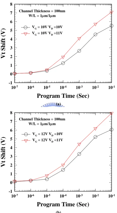
(13) different VD. (b) At VG=12V and different VD. The programming time can be as short as 10μs if the windows margin is set about 1V with VD=11V. Fig. 3-13 Program speed characteristic of different programming conditions for 1μm gate length and width, and 100nm channel thickness. (a) At VD=10V and different VG. (b) At VD=11V and different VG. When applying the same VD, that VG is increased doesn’t obviously improve program speed. Fig. 3-14 Program speed characteristic for different programming conditions. This gate length and width are both 0.8μm, and channel thickness is 100nm. (a) At VG=10V and different VD. (b) At VG=12V and different VD. The programming time can be as short as 10μs if the windows margin is set about 1V with VD=10V. Fig. 3-15 Program speed characteristic of different programming conditions for 0.8μm gate length and width, and 100nm channel thickness. (a) At VD=9V and different VG. (b) At VD=10V and different VG. When applying the same VD, that VG is increased doesn’t obviously improve program speed. Fig. 3-16 Erase speed characteristic for different erasing conditions. This gate length and width are both 1μm, and channel thickness is 50nm. (a) At VG=-10V and different VD. (b) At VG=-12V and different VD. The erasing time can be as short as μs order. Fig. 3-17 Erase speed characteristic of different erasing conditions for 1μm gate length and width, and 50nm channel thickness. (a) At VD=11V and different VG. (b) At VD=12V and different VG. Fig. 3-18 Erase speed characteristic for different erasing conditions. This gate length and width are both 0.8μm, and channel thickness is 50nm. (a) At VG=-10V and different VD. (b) At VG=-12V and different VD. The erasing time can be as short as μs order. Fig. 3-19 Erase speed characteristic of different erasing conditions for 0.8μm gate length and width, and 50nm channel thickness. (a) At VD=10V and different VG. (b) At VD=11V and different VG. Fig. 3-20 Erase speed characteristic for different erasing conditions. This gate length and width are both 1μm, and channel thickness is 100nm. (a) At VG=-10V and different VD. (b) At VG=-12V and different VD. The erasing time can be as short as μs order. Fig. 3-21 Erase speed characteristic of different erasing conditions for 1μm gate length and width, and 100nm channel thickness. (a) At VD=10V and different VG. (b) At VD=11V and different VG.. XI.
(14) Fig. 3-22 Erase speed characteristic for different erasing conditions. This gate length and width are both 1μm, and channel thickness is 100nm. (a) At VG=-10V and different VD. (b) At VG=-12V and different VD. The erasing time can be as short as μs order. Fig. 3-23 Erase speed characteristic of different erasing conditions for 0.8μm gate length and width, and 100nm channel thickness. (a) At VD=9V and different VG. (b) At VD=10V and different VG. Fig. 3-24 Endurance characteristic of 50nm channel thickness. This gate length and width are both 0.8μm. Memory window narrow to about 3V after 104 P/E cycles. Fig. 3-25 Endurance characteristic of 100nm channel thickness. This gate length and width are both 0.8μm. Memory window narrow to about 2V after 104 P/E cycles. Fig. 3-26 Data retention characteristic of high state and low state for 50nm channel thickness. This gate length and width are both 1μm. (a) At temperature T=25oC, and (b) at temperature T=85oC. Fig. 3-27 Data retention characteristic of high state and low state for 50nm channel thickness. This gate length and width are both 0.8μm. (a) At temperature T=25oC, (b) At temperature T=85oC. Fig. 3-28 Data retention characteristic of high state and low state for 100nm channel thickness. This gate length and width are both 1μm. (a) At temperature T=25oC, (b) At temperature T=85oC. Fig. 3-29 Data retention characteristic of high state and low state for 100nm channel thickness. This gate length and width are both 0.8μm. (a) At temperature T=25oC, (b) At temperature T=85oC. Fig. 3-30 Programming gate disturbance characteristic of 50nm channel thickness at VG=10V and VG=12V. (a) W/L=1μm/1μm, (b) W/L=0.8μm/0.8μm. The Vt shift of gate disturbance is lower than 0.3V for 1000s stress with VG=12V. Fig. 3-31 Programming gate disturbance characteristic of 100nm channel thickness at VG=10V and VG=12V. (a) W/L=1μm/1μm, (b) W/L=0.8μm/0.8μm. The Vt shift of gate disturbance is lower than 0.3V for 1000s stress with VG=12V. Fig. 3-32 Drain disturbance characteristic of 50nm channel thickness. (a) W/L=1μm/1μm at VD=11V and VD=12V, and (b) W/L=0.8μm/0.8μm at VD=10V and VD=11V. The Vt shift of drain disturbance is lower than 0.5V and 0.8V for (a) and (b) at the worse condition of 100sec stress, respectively. Fig. 3-33 Drain disturbance characteristic of 100nm channel thickness. (a) W/L=1μm/1μm at XII.
(15) VD=10V and VD=11V, and (b) W/L=0.8μm/0.8μm at VD=9V and VD=10V. The Vt shift of drain disturbance is lower than 0.4V for (a) and (b) at the worse condition of 100sec stress, respectively. Fig. 3-34 The characteristic of read multilevel operations. After once program, we use different VD to forward read and we will get different Vt due to drain-side shielded.. XIII.
(16) Chapter 1 Introduction 1.1 Brief Introduction of Poly-Si TFTs In 1966, the first polycrystalline silicon thin-film transistors (poly-Si TFTs) were fabricated by C.H. Fa et al. [1]. In recent years, poly-Si TFTs have drawn much attention because of their widely applications on active matrix liquid crystal displays (AMLCDs) [2], and organic light-emitting displays (OLEDs) [3]. Except large area displays, poly-Si TFTs also have been applied into some memory devices such as dynamic random access memories (DRAMs) [4], static random access memories (SRAMs) [5], electrical programming read only memories (EPROMs) [6], electrical erasable programming read only memories (EEPROMs) [7], linear image sensors [8], thermal printer heads [9], photo-detector amplifier [10], scanner, neutral networks [11]. Lately, some superior performances of poly-Si TFTs also have been reported by scaling down device dimension or utilizing novel crystallization technologies to enhance poly-Si film quality [12-13]. This provides the opportunity of using poly-Si TFTs into three dimension (3-D) integrated circuit fabrication. Of course, the application in AMLCDs is the primary trend, leading to rapid developing of poly-Si TFT technology. The major attraction of applying polycrystalline silicon thin-film transistors (poly-Si TFTs) in active matrix liquid crystal display (AMLCDs) lies in the greatly improved carrier mobility in poly-Si film and the capability of integrating the pixel switching elements and the capability to integrate panel array and peripheral driving circuit on the same substrates. [14-16] In poly-Si film, carrier mobility larger than 10 cm2/Vs can be easily achieved, that is enough to used as peripheral driving circuit including n- and p-channel devices. This enables the fabrication of peripheral circuit and TFT array on the same glass substrate, bring the era of. 1.
(17) system-on-plane (SOP) technology. The process complexity can be greatly simplified to lower the cost. In addition, the mobility of poly-Si TFTs is much better than that of amorphous ones; the dimension of the poly-Si TFTs can be made smaller compared to that of amorphous Si TFTs for high density、high resolution AMLCDs; and the aperture ratio in TFT array can be significantly improved by using poly-Si TFTs as pixel switching elements. This is because that the device channel width can be scaled down while meeting the same pixel driving requirements as in α-Si TFT AMLCDs. However, some problems still exist in applying poly-Si TFTs on large-area displays. In comparison with single-crystalline silicon, poly-Si is rich in grain boundary defects as well as intra-grain defects, and the electrical activity of the charge-trapping centers profoundly affects the electrical characteristics of poly-Si TFTs. Large amount of defects serving as trap states locate in the disordered grain boundary regions to degrade the ON current seriously [17]. Moreover, the relatively large leakage current is one of the most important issues of conventional poly-Si TFTs under OFF-state operation [18-19]. The dominant mechanism of the leakage current in poly TFTs is field emission via grain boundary traps due to the high electric field near the drain junction. To solve these problems, some crystallization methods, such as excimer laser annealing (ELA), has been introduced to enlarge the grain size [20]. A drain offset region or lightly-doped drain (LDD) region is used to effectively lower leakage current by decreasing drain electric field [21]. Up to date, some studies of poly-Si TFTs also focus on developing new technologies to lower the maximum fabrication temperature, which enables the use of low-quality glass and therefore reduce production cost [22]. Some reported papers focus on the fabrication and characterization of small-dimensional poly-Si TFTs [23], which has high driving ability and high resolution and can be applied on AMLCD peripheral circuitry or the high-resolution projectors. In summary, it is expected that the poly-Si TFTs will becomes more and more important in future technologies, especially when the 3-D circuit integration era comes. More researches studying the related new technologies and the 2.
(18) underlying mechanisms in poly-Si devices’ operation with shrinking dimensions are therefore worthy to be explored [24].. 1.2 Introduction of Non-Volatile Flash Memory In the past decade, Flash memory market has been driven by cellular phone and other types of electronic portable equipment (MP3 audio player, digital camera, and so on). It would further explosively grow in mass storage applications such as memory card and removable storage (e.g. USB Flash driver). Flash memory cell was firstly invented in 1984 [25]. It was realized by a 2μm triple poly-silicon technology with a cell size of 64μm2 to compose of a 256Kb chip [26]. It is based on the same concept of a floating-gate EPROM [27]. However, the erase is performed on a block of cells (or a whole chip) at the same time via electrical method. Such flash erase much increases the erase speed and thus earn the name after that [28]. The nonvolatility of semiconductor memory devices is usually achieved by charge storage in the multilayer gate structure of a field effect transistor or by polarizing the ferroelectric material in a ferroelectric capacitor/transistor. With respect to charge storage devices, there are two kinds of them. (a) Charge Trapping Devices: Charge is stored in the traps at the interfaces of a multilayer gate structure and/or in the insulator bulk, such as the metal nitride oxide silicon (MNOS) structure [29-30]. (b) Floating Gate Devices: Charge is stored in a thin conducting or semiconductor layer or conducting particles sandwiched between insulators [31-32]. Because of their lower endurance and retention, MNOS devices are used only in specific applications. On the contrary, floating gate devices are at the basis of every modern nonvolatile memory, and are used in particular for flash applications. Since the floating-gate concept is proposed in 1971 [33-34], Flash memories are destined to be the most powerful candidates for nonvolatile memories, which retain the data content even when the power is no longer supplied up to 10 years. Flash memories not only have the merits of dense 3.
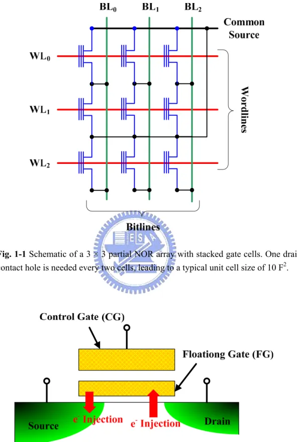
(19) integration of EPROM (which uses electrically programming and long-time UV erasure) but electrically erasure ability of EEPROM (which is a 2-transistor structure with electrically programming and erasing) [35]. Although many architectures are proposed, two main Flash architectures are NOR (such as Fig. 1-1) and NAND architectures. In 1999, the NOR architecture possesses almost 85% of Flash devices, but in recent year, great demands on mass storage application in mobile phones, digital cameras, and PDAs increase the NAND possession rate to almost the same rate of NOR. Both NOR and NAND structures are highly potential and full of profits from 2004. The stacked gate Flash memory is the most straight forward structure of floating gate device (see Fig. 1-2). Products with this structure in present market are mainly based on the ETOX concept (EPROM with thin oxide), which was proposed by Intel in 1984 [36]. Programming is performed by channel hot electron injection occurred near the drain side with control-gate voltage (VCG), drain voltage (VD), typically, in several μs. Erasure is achieved by Folwer-Nordheim (FN) tunneling from FG to source or to both source and channel regions in a range of ms to a few seconds. Two erase schemes are classified by VCG: (i) grounded gate source erase and (ii) negative gate source erase. As the naming, the negative gate erase will use a smaller source voltage than that of grounded gate erase for the same oxide field magnitude. The latter scheme has the advantages of larger margin with respect to breakdown voltage limitation in source-substrate junction and large tolerance on band-to-band tunneling leakage. The band-to-band tunneling (BTBT) is remarkable when a large positive bias is applied on source (VS) in grounded gate erase (see Fig. 1-3). The parasitic current demands a large current for common source structure during erasure; moreover, the high VS may cause some BTBT generated holes being accelerated by lateral field (source to substrate) to a high energy. Afterwards, some hot holes will be injected into tunnel oxide and degrade the device with transconductance lowering, overerase problems, and poor endurance characteristics [37]. 4.
(20) Although the negative gate erase has so many advantages, drawback exists due to the circuit overhead from additional on-chip charge pump for negative gate erase scheme [38].. 1.3 Motivation Development of the “System-on-Plane” (SOP) display with low temperature Poly-Si (LTPS) TFTs has rapidly advanced recently. The LTPS TFT LCDs achieve high resolution, high luminance displays, which allow us to integrate various functional circuits onto the display panels. The new functional devices fabricated on the glass can increase the flexibility of circuits for the display. The display based on above opinion incorporated with nonvolatile memories becomes an attractive topic recently. Low-temperature poly-Si nonvolatile memory can provide us a new direction to integrate analogue and digital display circuits for the display system. However, up to date, there are a few reports that focus on nonvolatile memories using LTPS TFTs on glass. In order to overcome the scaling limits of the conventional FG structure, and compatible with low temperature TFTs process. We proposed a Ge trapping layer for low temperature poly-Si TFTs with a low operating voltage and significant threshold-voltage shift. Compared with conventional in-situ Si floating gate, deposition temperature of Si layer is higher and doped Si floating gate thickness is thicker. So Si FG memory has larger operating voltage and critically scaling issue. On the other hand, Ge has a narrower bandgap and a similar electron affinity [39], and trapping ability of Ge layer is better than Si FG. Deposition temperature of Ge layer is lower about 400oC. It is appropriate for low temperature poly-Si TFTs process. The Ge layer has better trapping ability without doping, so it need only very thin layer. For scaling issue, Ge trapping layer will be the candidate of future LTPS nonvolatile TFTs memory. In this thesis, we also discuss program and erase mechanism for thin film device. The SOI and TFTs are also floating body devices, and because of floating body, it will cause drain avalanche to occur early. So we utilized impact ionization of drain 5.
(21) avalanche to improve carrier injection efficiency and program/erase speed. Also we can reduce operation voltage. We demonstrated that LTPS TFTs with Ge trapping layer can be scale down, reduce program/erase voltage and improve program/erase speed.. 1.4 Organization of This Thesis The organization of this thesis is separated into four chapters. After a brief introduction in Chapter 1, we will introduce the devices fabrication, experimental measurement, the basic property of thin film transistor including the parameter extraction, program/erase mechanism. And we will discuss the influence of floating body drain avalanche in Chapter 2. In Chapter 3, we demonstrated a nonvolatile memory on low temperature polycrystalline silicon TFTs with Ge trapping layer. We will show the basic characteristics of the SOGOS memory and compare the device performance with various channel film thickness and device dimension, including program/erase speed, endurance, data retention, gate disturbance and drain disturbance. Finally, the conclusion and future work are given in Chapter 4.. 6.
(22) Fig. 1-1 Schematic of a 3 × 3 partial NOR array with stacked gate cells. One drain contact hole is needed every two cells, leading to a typical unit cell size of 10 F2.. Fig. 1-2 Schematic cross sectional view of stacked gate Flash memory cell along cell channel direction. The channel hot electron programming near drain side and FN-tunneling source erase are symbolized with arrows. 7.
(23) VCG ≤ 0V. VS< 0V. BTBT region. Source. Depletion layer edge. Fig. 1-3 Schematic illustration shows the band-to-band tunneling (BTBT) phenomenon in circled region when there is a high gate to source bias.. 8.
(24) Chapter 2 Experimental Procedures and Device Operations 2.1 Device Fabrication The schematic diagram of the fabrication process is illustrated in Fig. 2-1. First, a 550-nm thick oxide was deposited on the (100) 6-inch wafers. Then, a 50-nm and 100-nm thick a-Si layer was deposited as the active layer in a LPCVD system using SiH4 as source at 550°C. The a-Si was crystallized to poly-Si by solid phase crystallization (SPC) process at 600°C for 24 hours. Then the wafers were subjected to photolithography for active region definition. After a standard RCA cleaning, we deposited 11-nm TEOS oxide as tunneling oxide. Then, we deposited a thin a-Si layer, and deposited a thin Ge layer in LPCVD system using GeH4 at low temperature as trapping layer. A blocking oxide about 44nm was then deposited using TEOS oxide. A 200-nm thick a-Si was deposited to serve as the gate electrode by LPCVD. Subsequently, the n+ gate was formed by ion implantation of phosphorous at 10 keV to a dose of 5x1015 cm-2. Then the a-Si gate electrode and the Ge/Si trapping layer with tunneling oxide were etched by poly-Si dry etcher (TCP- 9400) and the oxide dry etcher (TEL-5000), respectively. The wafers were ion implanted by phosphorous. The energy and the dose of implantation were 15 keV to dose 5×1015 cm-2 and 25kev to dose 5×1015 cm-2 for channel thickness 50-nm and 100-nm , respectively. Then, the n+ gate, n+ source and n+ drain region were activated at 600oC for several hours (? hour). At the same time, n+ a-Si gate was crystallized to n+ poly-Si gate. During this activation period, the previously deposited Ge trapping layer recrystallized and then formed into nanocrystals, which were embedded in oxide. As shown Fig. 2-2, the cross-sectional TEM image of the gate stack shows Ge nanocrystal embedded oxide. The. 9.
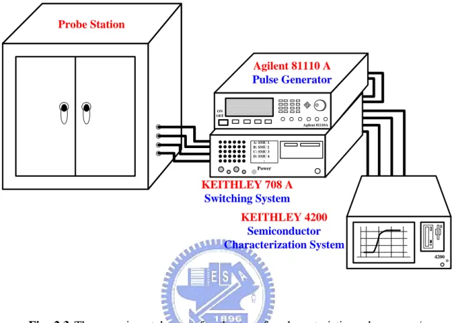
(25) nanocrystal size was estimated about diameter of 11 nm in average. Next, a 300-nm thick TEOS oxide was deposited as passivation layer and patterned for contact holes opening. A 500-nm thick Al was immediately thermal evaporated, followed by lithography for Al pad pattern definition. The LTPS TFTs with Ge trapping layer memory was finished.. 2.2 Typical Threshold Voltage Parameter Extraction In this section, the methodology of extracting typical parameters, such as threshold voltage from device characteristics, are briefly introduced. Plenty ways are used to determinate the threshold voltage which is the most important parameter of semiconductor devices. The method to determinate the threshold voltage in my thesis is the constant drain current method that the voltage at a specific drain current IN is taken as the threshold voltage. This technique is easy and can give a threshold voltage close to that obtained by the complex linear extrapolation method. Typically, the threshold current IN = IDN / (W / L) where IDN is a normalized drain current. Here, IDN is 100 nA and the same for all devices to extract the threshold voltage of TFTs [40].. 2.3 Measurement Equipment Setup The experimental setup for the I-V and threshold voltage characteristics measurement of the LTPS TFTs with Ge nanocrystal is illustrated in Fig. 2-3. As shown in Fig. 2-3, the characterization apparatus with semiconductor characterization system (KEITHLEY 4200), one channel pulse generator (Agilent 81110A), low leakage switch mainframe (KEITHLEY 708A), and a probe station provide an adequate capability for measuring the device I-V characteristics and executing the non-volatile memory cell program/erase operation. The KEITHLEY 4200 equipped with programmable source-monitor units and provides a high current resolution to pico-ampere range facilitates the gate current measurement, subthreshold characteristics extraction, and the saturation drain current. 10.
(26) measurement. The one channel Agilent 81110A with high timing resolution provides one pulse level for transient and P/E cycling endurance characterization. Another pulse level is provided by KEITHLEY 4200. The KEITHLEY 708A configured a 10-input×12-output switching matrix, switches the signals from the KEITHLEY 4200 and the Agilent 81110A to device under test in probe station, automatically. In addition, the C++ is used as the program language to achieve the KEITHLEY 4200 control of these measurement instruments [41].. 2.4 Program and Erase Operation In the past, several methods have been proposed to transport electrons into the trapping layer. The method of BBHE (Band-to-Band Hot Electron), however, is the most widely used one to program the n-channel flash memory wing to its features of higher efficiency and lower power dissipation. By applying a positive drain voltage and a positive control gate voltage to the cell, electron-hole pairs are generated by band-to-band tunneling in the deep depletion region. Subsequently, the electrons are accelerated by a lateral electric field towards the channel region and some of them will gain sufficient energy. The injection of such hot electrons into the trapping layer through the tunnel oxide is called the BBHE programming method. The major advantage of this method is its high efficiency, since electrons are generated by band-to-band tunneling and efficiently accelerated by the lateral electric field in the drain deep depletion region [42]. In our measurement, we use disadvantage of thin-film device that is floating body effect. The floating body effect will cause induced drain avalanche to occur early at high voltage. This behavior, called the floating body drain avalanche, will more improve program speed. In the next chapter, we will discuss this program mechanism particularly. In general, the erase operation is intended to remove electrons from the trapping layer to bring the device back to its initial low threshold voltage state. Fowler-Nordheim tunneling of electrons is generally used to erase the flash memory. The control gate is applied with a. 11.
(27) negative voltage with respect to the substrate so that FN currents flow through the gate oxide more or less uniformly over the entire channel. The charge conduction over the entire channel during the high field FN erase operation will damage the main channel and thus results in the detrimental drawbacks, such as the worse endurance and disturbs in the flash array. In addition, the generation and switching of negative voltages during erase will make the circuit design be more complicate [42]. In our measurement, we use Band-to-Band hot hole that produced by a great deal electron-hole pairs of drain avalanche. This mechanism will more improve erase speed. In the next chapter, we will discuss this erase mechanism particularly.. 2.5 Endurance and Retention Today flash memory cells are requested to guarantee 100,000 program/erase cycles. Cycling is known to cause fairly uniform wear-out of cell performance due to the oxide damage. This experiment was performed by applying VCG=10V, VD=11V, and VS =0V during programming. After programming, erasing pulses are applied with drain current and with VCG=-11V, VS= 10V, and VS=0. The threshold voltage is measured after some program/erase cycles. The “threshold voltage window closure” is due to the traps and interface states generated during program/erase cycles. The reduction of the programmed threshold with cycling is due to trap generation in the oxide and to interface state generation at the drain side of the channel, which are usually called hot electron degradations. The evolution of erase threshold voltage reflects the dynamics of net fixed charge in the tunnel oxide as a function of the injected charge [43]: the initial lowering of the erased threshold voltage is due to positive trapped charge which enhances tunneling efficiency, while the long term increase of the erased threshold voltage is due to generation of negative traps. The cycled program/erase operations will cause the oxide degradation and lower the potential well barrier surrounding the floating gate. Hence the stored charge loss and gain in the floating gate may limit the tunneling oxide. Retention capability of flash memories has to be checked by using. 12.
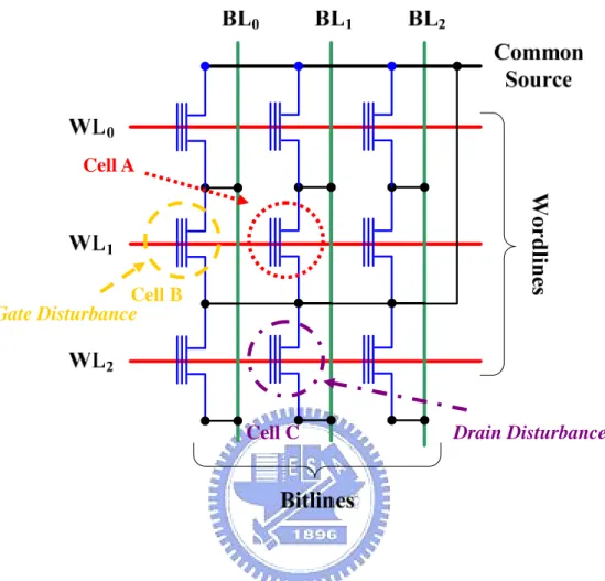
(28) accelerated test that usually adopts high electric fields and high temperature [44].. 2.6 The Disturbance The first failure phenomenon, called program disturbance, often takes place under the electric stress applied to those neighboring un-programmed cells during programming a specific cell in the array. Two types of program disturbance, gate (word-line) disturbance and drain (bit-line) disturbance need be considered. The schematic circuitry of the memory array is shown in Fig. 2-4. During programming cell A, gate disturbance occurs in the cell B and the same for those cells connected with the same with word-line because the gate stress is applied to the same word-line (WL). This is called gate disturbance. During programming cell A, drain disturbance occurs in the cell C and the same for those cells connected with the same with bit-line because the drain stress is applied to the same bit-line (BL). This is called drain disturbance. For the cell reading, the unwanted electron injection would happen while the word-line voltage and bit-line voltage are under read operation. This phenomenon would result in a significant threshold voltage of the selected cell. This is called read disturbance [45].. 13.
(29) Wet Oxidation 550nm on (100) Si Wafer. Deposited a-Si 50/100nm as Active Layer.. Solid Phase Crystallization at 600oC 24hr and Defined Active Region.. Deposited TEOS 11nm as Tunneling Oxide. Deposited a-Si /Ge as Trapping Layer. Deposited TEOS 44nm as Blocking Oxide. Deposited a-Si 200nm as Gate Layer and P + Implantation.. Gate Pattern Defined and Soure/Drain P + Implantation.. 14.
(30) Fig. 2.1 Process flows of low temperature poly-Si TFTs. After deposited 300nm passvation oxide, dopant activation, metallization, and NH3 plasma treatment, we had finished device fabrication. During the dopant activation step, the Ge trapping layer was recrystallized and Ge nanocrystals embedded oxide were formed.. 15.
(31) at e G i -S Poly e d i x gO n i k Bloc e. Oxid g n i l el ne n n Tun a h. iC S y l Po (a). Ge Nanocrystal (b) Fig. 2.2 (a) Cross-sectional TEM image of the gate stack. (b) The Ge nanocrystals with about diameter of 11nm are formed on the TEOS tunneling oxide.. 16.
(32) Probe Station. Agilent 81110 A Pulse Generator ON OFF Agilent 81110A. A: SMU 1 B: SMU 2 C: SMU 3 D: SMU 4 :. Power. KEITHLEY 708 A Switching System KEITHLEY 4200 Semiconductor Characterization System 4200. Fig. 2.3 The experimental setup for the transfer characteristic and program/erase characteristic of LTPS TFTs with Ge nanocrystals memory.. 17.
(33) Cell A. Cell B Gate Disturbance. Drain Disturbance. Cell C. Fig. 2.4 During Cell A is programmed, the gate disturbance takes place in Cell B and the drain disturbance takes place in Cell C.. 18.
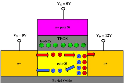
(34) Chapter 3 Electrical Characteristics of TFT Flash Memory 3.1 Program and Erase Mechanisms In this section, we will discuss the program and erase injection mechanism. The programming scheme is executed by using floating body induced drain avalanche hot electron and channel hot electron to injection charge into the Ge-NCs trapping layer. This program mechanism is different form drain avalanche hot electron in the bulk MOSFETs. On the other hand, the erasing scheme is executed by using Band-to-Band hot holes injection [43] to combine negative charge in the trapping layer. The injection components and efficiency for different gate bias and drain bias conditions on devices with different channel thickness will be discussed.. 3.1.1. Floating Body Effect Induced Drain Avalanche in Poly-Si Thin Film Transistors The drain avalanche is a kind of junction breakdown mechanism. And it needs. different drain bias for the bulk MOSFETs and thin-film device. For the bulk MOSFETs, it must apply large drain voltage to form reverse pn junction bias and then drain avalanche will occur. But for thin-film device, such as SOI or TFTs that has floating body, floating p-base is similar to the known “snap-back” mechanism of MOS transistor [44]. When applying drain bias and zero gate bias, the hole of impact ionization at depletion region of drain-side will flow into source and then additional electron will flow into depletion region of drain-side form source in return. This phenomenon will induce drain avalanche to occur early. So it can be occurred drain avalanche at smaller drain bias for SOI devices or TFTs. In general, we hope to avoid this situation for normal device operations because it will make our device breakdown early. Fig. 3-1 shows illustration of floating body effect in a TFT device, when 19.
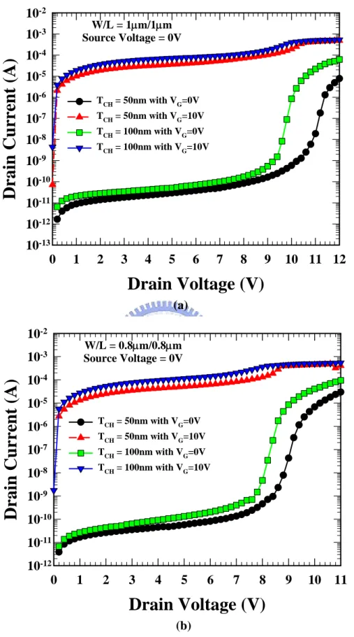
(35) VG=VS is 0V and VD is 12V. Applying smaller drain bias, we can get a great deal of electron-hole pairs due to drain avalanche before junction breakdown. We use the mechanism of floating body induced drain avalanche for program mode. Fig. 3-2 shows illustration of floating body effect induced drain avalanche hot electron injection in a TFT memory, when VG=10V, VS=0V and VD=12V. The avalanche current serves as the “base” current and the bipolar action contributes additional current flowing through the drain side and additional hot electrons generated for injection. Some of them with energy higher than the barrier height of SiO2/Si conduction band, so they can surmount the barrier and are injected into the trapping layer. Fig. 3-3 shows drain avalanche current for 50nm channel thickness with different gate width of 1μm and 10μm, and at different VG=0V and VG=10V. (a) When VD is larger than 10V, we can observe a suddenly large drain current for 1μm Gate length. (b) When VD is larger than 8.4V, we can also observe a suddenly large drain current for 0.8μm gate length. When gate length is smaller, drain avalanche voltage is lower. And we also define program region of drain bias from Fig. 3-3. Fig. 3-4 shows drain avalanche current for 100nm channel thickness with different gate width 1μm and 10μm, and different VG=0V and VG=10V. (a) When VD is larger than 8.4V, we can observe a suddenly large drain current for 1μm gate length. (b) When VD is larger than 8V, we can also observe a suddenly large drain current for 0.8μm gate length. When gate length is smaller, drain avalanche voltage is also lower. The same as 50nm channel thickness, we also define program region of drain bias. According to all of the above, the floating body effect is more serious for 100nm channel thickness than 50nm. So the floating body induced drain avalanche will occur early for 100nm channel thickness and it has more low programming voltage for 0.8μm gate length and 100nm channel thickness. Fig. 3-5 shows comparison for drain avalanche current of different channel thickness and VG, (a) gate length and width are both 1μm, and (b) gate length and width are both 0.8μm. If program voltage is set at VG=10V, Fig. 3-6 shows the linear characteristic of program current and comparison of different channel thickness. (a) 20.
(36) Gate length and width are both 1μm, and (b) gate length and width are both 0.8μm. In n-channel, when a negative gate bias and a positive drain bias are applied to the cell, electron-hole pairs are generated in the drain region. The channel hole current will be accelerated by a lateral electric field toward the channel region. And heated holes will be generated and be injected by band-to-band into the gate at the gate-drain overlap region [45]. The injection of such hot holes into Ge-NCs trapping layer through the tunnel oxide is used for erase operation in our TFTs memories.. 3.1.2. Transfer Characteristic of Program/Erase State The floating body effect induced drain avalanche (FBDA) hot electrons injection and. Band-to-Band hot holes injection were employed for programming and erasing mode, respectively. Fig. 3-7 shows the transfer characteristic of erase state and program state for 0.8μm gate length and width. (a) Channel thickness is 50nm, and (b) channel thickness is 100nm. We clearly observed that memory window is quite large. Applying VG=10V, VD=11V and VG=VD=10V, a memory window larger than 8V can be easily achieved for TCH=50nm and TCH=100nm, respectively, when program time is 1sec. When channel thickness is 50nm, leakage current of program state is lower. Because it has more defects in thin channel thickness than thick one, the leakage current of 50nm channel thickness is low about 10-12A.. 3.2 Characteristics of Program/Erase In this section, we will discuss the program speed of floating body effect induced drain avalanche hot electrons injection mode and erase speed of band-to-band hot holes injection mode, respectively.. 3.2.1. Program Speed Fig. 3-8(a)-(b) exhibits program speed characteristic for different programming. conditions. This gate length and width are both 1μm, and channel thickness is 50nm. We changed drain voltage bias with 11V and 12V to measure program speed at fixed 10V and. 21.
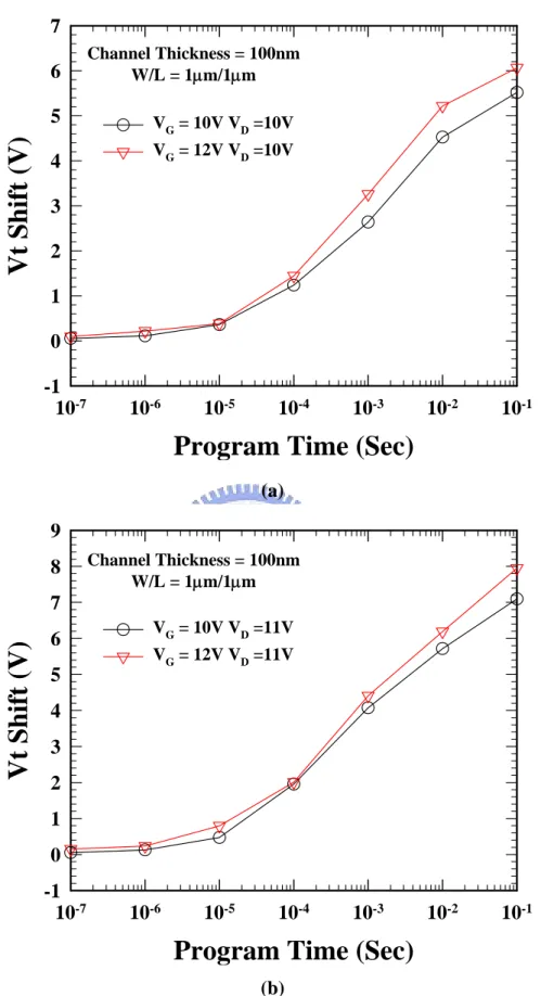
(37) 12V gate voltage bias, respectively. We can see that the programming time can be as short as 10μs if the windows margin is set about 1V with VD=12V for two cases at fixed 10V and 12V gate bias. Fig. 3-9(a)-(b) shows program speed characteristic, when we changed gate voltage bias with 10V and 12V to measure program speed for fixed 11V and 12V drain voltage bias respectively. For the same VD, that VG is increased doesn’t obviously improve program speed. Fig. 3-10(a)-(b) exhibits program speed characteristic for different programming conditions. This gate length and width are both 0.8μm, and channel thickness is 50nm. We also changed drain voltage bias with 10V and 11V to measure program speed for fixed 10V and 12V gate bias respectively. We can also see that the programming time can be as short as 10μs if the windows margin is set about 1V with VD=11V for two cases of fixed 10V and 12V gate bias. Fig. 3-11(a)-(b) shows program speed characteristic, when we changed gate voltage bias with 10V and 12V to measure program speed for fixed 10V and 11V drain voltage bias respectively. For the same VD, that VG is increased doesn’t also obviously improve program speed. Fig. 3-12(a)-(b) exhibits program speed characteristic for applying drain voltage bias with 10V and 11V, then fixed 10V and 12V gate voltage bias respectively. This gate length and width are both 1μm, and channel thickness is 100nm. The programming time can be as short as 10μs if the windows margin is set about 1V when applying VD=11V. Fig. 3-13(a)-(b) shows program speed characteristic for applying gate voltage bias with 10V and 12V, then fixed 10V and 11V drain voltage bias respectively. When applying the same VD, that VG is increased doesn’t also obviously improve program speed. Fig. 3-14(a)-(b) exhibits program speed characteristic for applying drain voltage bias with 9V and 10V, then fixed 10V and 12V gate voltage bias respectively. This gate length and width are both 0.8μm, and channel thickness is 100nm. The programming time can be as short as 10μs if the windows margin is set about 1V when applying VD=10V. Fig. 3-15(a)-(b) shows program speed characteristic for applying gate voltage bias with 10V and 12V, then fixed 9V and 10V drain voltage bias respectively. For the same VD, that VG is increased doesn’t obviously improve program speed. 22.
(38) In conclusion, Table 3-1 and Table 3-2 show summary for program memory window of 1ms program time, and compare fixed VG=10V and VG=12V for all cases of different VD. For all cases, we use two kind of drain voltage bias for strong and weak drain avalanche, respectively. It can be clearly seen that larger drain bias induced strong drain avalanche makes faster program speed. On the other hand, the gate bias only supplies a vertical field to hot electrons for injected into the trapping layer so the influence of increased gate voltage is not conspicuous. The smaller gate length needs only lower program voltage for the same Vt shift. This is called gate length effect. And the program voltage is lower for 100nm channel thickness than 50nm, because the drain avalanche voltage is lower for 100nm channel thickness, as shown in Fig. 3-5. According to all of the above, we can clearly observe that FBDA can improve injection efficiency and get faster program speed.. 3.2.2. Erase Speed Fig. 3-16(a)-(b) shows erase speed characteristic for different erasing conditions. The. gate length and width are both 1μm, and channel thickness is 50nm. We changed drain voltage bias with 11V and 12V to measure erase speed for fixed -10V and -12V gate voltage bias respectively. We can see that erasing time can be as short as μs in order to combine negative charge in the trapping layer. Fig. 3-17(a)-(b) exhibits erase speed characteristic when we changed gate voltage bias with -10V and -12V to measure erase speed for fixed 11V and 12V drain voltage bias respectively. The increased gate bias does not obviously accelerate erase speed. Fig. 3-18(a)-(b) shows erase speed characteristic for different erasing conditions. This gate length and width are both 0.8μm, and channel thickness is 50nm. We changed also drain voltage bias with 10V and 11V to measure erase speed for fixed -10V and -12V gate voltage bias respectively. We can clearly see that the μs order of erasing time can combine negative charge in the trapping layer. Fig. 3-19(a)-(b) exhibits erase speed characteristic when we changed gate voltage bias with -10V and -12V to measure erase speed for fixed 10V and 11V drain voltage bias respectively. The erase speed of different gate bias is almost the same. 23.
(39) Fig. 3-20(a)-(b) shows erase speed characteristic for applying drain voltage bias with 10V and 11V, then fixed -10V and -12V gate voltage bias respectively. The gate length and width are both 1μm, and channel thickness is 100nm. Fig. 3-21(a)-(b) exhibits erase speed characteristic for applying gate voltage bias with -10V and -12V, then fixed 10V and 11V drain voltage bias respectively. Fig. 3-22(a)-(b) shows erase speed characteristic for applying drain voltage bias with 9V and 10V, then fixed -10V and -12V gate voltage bias respectively. The gate length and width are both 1μm, and channel thickness is 100nm. Fig. 3-23(a)-(b) exhibits erase speed characteristic for applying gate voltage bias with -10V and -12V, then fixed 9V and 10V drain voltage bias respectively. In conclusion, Table 3-3 and Table 3-4 show summary for erase Vt shift of 100ms erase time, and compared at fixed VG=-10V and VG=-12V for all cases of different VD. The gate bias supplies only a vertical field to collect hot holes for combined negative charge in the trapping layer so the influence of increased gate voltage is not obvious. On the other hand, for all cases, we use two kind of drain voltage bias for strong and weak impact ionization at depletion of drain-side, respectively. It can be clearly seen that larger drain bias induced strong impact ionization makes faster erase speed. The erase voltage is lower for 100nm channel thickness than 50nm ones. And the smaller gate length needs only lower erase voltage for the same Vt shift. According to all of the above, we can clearly observe that our LTPS TFT memory with Ge-NCs trapping layer has very higher hot holes injection efficiency and faster erase speed.. 3.3 Characteristics of Retention and Endurance In this section, we will discuss program/erase cycles called endurance and data retention for device with different size, channel thickness and temperature. The flash memory cells are requested to guarantee 100,000 program/erase cycles. Cycling is known to cause fairly uniform wear-out of cell performance due to the oxide damage. Fig. 3-24 shows. 24.
(40) endurance characteristic of 50nm channel thickness. This gate length and width are both 0.8μm. We can clearly see that the memory window narrows to about 3V after 104 P/E cycles. And Fig. 3-25 exhibits endurance characteristic of 100nm channel thickness. The gate length and width are both 0.8μm. Also we can clearly see that the memory window narrows to about 2V after 104 P/E cycles. The “threshold voltage window closure” is due to the traps and interface states generated during program/erase cycles. The reduction of the programmed threshold with cycling is due to trap generation in the oxide and to interface state generation at the drain side of the channel, which are usually called hot electron degradations. While the long term, increase of the erased threshold voltage is due to generation of negative traps. And both the swing became larger after 104 P/E cycles. In our device, the memory window still maintains quite larger than 2V even through inflicted 104 P/E cycles. Data retention is an important reliability issue of TFT flash memories. In general, retention capability of flash memories has to be checked by using accelerated test that usually adopts high electric fields and high temperature. Fig. 3-26 shows data retention characteristic for device with W/L=1μm /1μm and 50nm channel thickness. Fig. 3-27 exhibits data retention characteristic for device with W/L=0.8μm /0.8μm and 50nm channel thickness. Fig. 3-28 shows data retention characteristic for device with W/L=1μm /1μm and 100nm channel thickness. And Fig. 3- 29 exhibits data retention characteristic for device with W/L=0.8μm /0.8μm and 100nm channel thickness. For above cases, we measured the situation of data retention at temperature T=25oC and T=85oC, respectively. For temperature T=25oC, all cases presented good retention characteristics but charge loss is serious for TCH=100nm than TCH=50nm for their high state. This also shows that the trapping capability of Ge-NCs trapping layer is very excellent. On the other hand, we observed larger charge loss percentage for ten years when using accelerated test at temperature T=85oC. This charge loss is due to the poor quality of tunnel oxide which results in many leakage current path.. 25.
(41) 3.4 Characteristics of Disturbance In this section, we will discuss characteristics of disturbance for devices with different size and channel thickness. The first failure phenomenon, program disturbance, often takes place under the electrical stress applied to those neighboring un-programmed cells during programming a specific cell in the array. Two types of program disturbance, gate (word-line) disturbance and drain/source (bit-line) disturbance need to be considered. Fig. 3-30(a)-(b) shows programming gate disturbance characteristic of 50nm channel thickness with VG=10V and VG=12V for W/L=1μm/1μm and W/L=0.8μm/0.8μm, respectively. The Vt shift of gate disturbance is lower than 0.3V for 1000s stress with VG=12V. Fig. 3-31(a)-(b) exhibits programming gate disturbance characteristic of 100nm channel thickness with VG=10V and VG=12V for W/L=1μm/1μm and W/L=0.8μm/0.8μm. The Vt shift of gate disturbance can also be controlled lower than 0.3V for 1000s stress with VG=12V. After gate electrical stress applied for a long time, it resulted in a decrease of threshold voltage. This may be attributed to poor quality of blocking oxide which results in the holes gate injection. And Fig. 3-32(a)-(b) shows drain disturbance characteristic of 50nm channel thickness for W/L=1μm/1μm with VD=11V and VD=12V, and W/L=0.8μm/0.8μm with VD=10V and VD=11V. The Vt shift of drain disturbance is lower than 0.5V and 0.8V for (a) and (b) at the worse condition of 100sec stress, respectively. Fig. 3-33(a)-(b) exhibits drain disturbance characteristic of 100nm channel thickness for W/L=1μm/1μm with VD=10V and VD=11V, and W/L=0.8μm/0.8μm with VD=9V and VD=10V. The Vt shift of drain disturbance is lower than 0.4V for (a) and (b) at the worse condition of 100sec stress, respectively. After drain electrical stress applied a long time, it resulted in a increase of threshold voltage. It might be due to two factors: The first is due to poor quality of blocking and tunnel oxide result in the gate injection. The other is due to that drain electrical stress applied along long time resulted in the traps and interface states generated at drain-side, and subthreshold swing became larger.. 26.
(42) 3.5 2-Bits Operation In this section, we will discuss multi-bit operation for our LTPS TFTs with Ge-NCs trapping layer. We demonstrated the feasibility of multi-bit operation with different VD of forward read scheme in a single cell for our TFT memory. Fig. 3-34 shows characteristic of read multilevel operations. After once program, we use different VD to forward read and got different threshold voltage. Table 3-5 exhibits summary for read multilevel operation. The interval of each state is larger than 1.4V. This phenomenon is believed due to that charge trapped by localization. The different threshold voltages were observed while we use the forward reading operation. The main reason for this phenomenon was that the different drain voltage biases were applied in our device resulted in different depletion width near the drain-side, thus, the different depletion width near the drain-side will shielded the different localized charge trapping positions. So we use forward read with different VD and then can get different threshold voltage.. 27.
(43) VG = 0V. n+ poly Si. VS = 0V. VD = 12V. TEOS. Ge-NCs. e-. n+. e-. poly-Si h+. h+. e-. h+. e-. h+. e-. h+. e-. n+. h+. Buried Oxide. Fig. 3-1 Illustration of floating body effect in a TFT device, when VG=VS is 0V and VD is 12V.. Fig. 3-2 Illustration of floating body effect induced drain avalanche hot electron injection in a TFT memory, when VG=10V, VS=0V and VD=12V. And the mechanism of additional injection due to the floating base of the parasitic npn bipolar. 28.
(44) 10-2. Drain Current (A). 10-3. Channel Thickness = 50nm Source Voltage = 0V. 10-4 10-5 10-6. W/L = 10μm/1μm with VG=0V. 10-7. W/L = 1μm/1μm with VG=0V. 10-8. W/L = 10μm/1μm with VG=10V W/L = 1μm/1μm with VG=10V. 10-9 10-10 10-11. Program Region. 10-12 10-13 0. 1. 2. 3. 4. 5. 6. 7. 8. 9 10 11 12 13. Drain Voltage (V) (a). 10-2. Drain Current (A). 10-3. Channel Thickness = 50nm Source Voltage = 0V. 10-4 10-5 W/L = 10μm/0.8μm with VG=0V. 10-6. W/L = 0.8μm/0.8μm with VG=0V. 10-7. W/L = 10μm/0.8μm with VG=10V W/L = 0.8μm/0.8μm with VG=10V. 10-8 10-9. Program Region. 10-10 10-11 10-12 0. 1. 2. 3. 4. 5. 6. 7. 8. 9. 10. 11. Drain Voltage (V) (b) Fig. 3-3 Drain avalanche current for 50nm of channel thickness with different width and VG, (a) gate length is 1μm, and (b) gate length is 0.8μm. When gate length is smaller, drain avalanche voltage is smaller.. 29.
(45) 10-2. Drain Current (A). 10-3. Channel Thickness = 100nm Source Voltage = 0V. 10-4 10-5 W/L = 10μm/1μm with VG=0V. 10-6. W/L = 1μm/1μm with VG=0V. 10-7. W/L = 10μm/1μm with VG=10V W/L = 1μm/1μm with VG=10V. 10-8 10-9 10-10. Program Region. 10-11 10-12 0. 1. 2. 3. 4. 5. 6. 7. 8. 9. 10. 11. Drain Voltage (V) (a). 10-1. Drain Current (A). 10-2. Channel Thickness = 100nm Source Voltage = 0V. 10-3 10-4 10-5. W/L = 10μm/0.8μm with VG=0V. 10-6. W/L = 0.8μm/0.8μm with VG=0V. 10-7. W/L = 10μm/0.8μm with VG=10V W/L = 0.8μm/0.8μm with VG=10V. 10-8 10-9 10-10. Program Region. 10-11 10-12 0. 1. 2. 3. 4. 5. 6. 7. 8. 9. 10. 11. Drain Voltage (V) (b) Fig. 3-4 Drain avalanche current for 100nm channel thickness with different width and VG, (a) gate length is 1μm, and (b) gate length is 0.8μm. When gate length is smaller, drain avalanche voltage is smaller.. 30.
(46) 10-2 W/L = 1μm/1μm Source Voltage = 0V. Drain Current (A). 10-3 10-4 10-5 10-6. TCH = 50nm with VG=0V. 10-7. TCH = 50nm with VG=10V TCH = 100nm with VG=0V. 10-8. TCH = 100nm with VG=10V. 10-9 10-10 10-11 10-12 10-13 0. 1. 2. 3. 4. 5. 6. 7. 8. 9. 10 11 12. Drain Voltage (V) (a). 10-2 W/L = 0.8μm/0.8μm Source Voltage = 0V. Drain Current (A). 10-3 10-4 10-5 10-6. TCH = 50nm with VG=0V. 10-7. TCH = 100nm with VG=0V. 10-8. TCH = 100nm with VG=10V. TCH = 50nm with VG=10V. 10-9 10-10 10-11 10-12 0. 1. 2. 3. 4. 5. 6. 7. 8. 9. 10. 11. Drain Voltage (V) (b) Fig. 3-5 Comparison for drain avalanche current of different channel thickness and VG, (a) gate length and width are 1μm, and (b) gate length and width are 0.8μm. The floating body induced drain avalanche will occur more early for 100nm channel thickness. 31.
(47) 0.6. Drain Current (mA). W/L = 1μm/1μm Source Voltage = 0V. 0.5 TCH = 50nm with VG=10V TCH = 100nm with VG=10V. 0.4 0.3 0.2 0.1 0.0 0. 1. 2. 3. 4. 5. 6. 7. 8. 9. 10 11 12. Drain Voltage (V) (a). 0.6. Drain Current (mA). W/L = 0.8μm/0.8μm Source Voltage = 0V. 0.5 TCH = 50nm with VG=10V. 0.4. TCH = 100nm with VG=10V. 0.3 0.2 0.1 0.0 0. 1. 2. 3. 4. 5. 6. 7. 8. 9. 10. Drain Voltage (V) (b) Fig. 3-6 The linear characteristic of program current and comparison of different channel thickness with 10V gate voltage. (a) Gate length and width are 1μm, and (b) gate length and width are 0.8μm.. 32.
(48) Drain Current ID (A). 10-4 Channel Thickness = 50nm Erase State W/L = 0.8μm/0.8μm VG=10V, VD=11V, 1sec. 10-5 10-6 10-7 10-8 10-9 10-10 10-11 10-12 -6. -4. -2. 0. 2. 4. 6. 8. 10. Gate Voltage VG (V) (a). Drain Current ID (A). 10-4 Channel Thickness = 100nm Erase State W/L = 0.8μm/0.8μm VG=10V, VD=10V, 1sec. 10-5 10-6 10-7 10-8 10-9 10-10 10-11 10-12 -6. -4. -2. 0. 2. 4. 6. 8. 10. Gate Voltage VG (V) (b) Fig. 3-7 Transfer characteristic of erase state and program state, when gate length and width is both 0.8μm. (a) Channel thickness is 50nm, and (b) channel thickness is 100nm. A memory window larger than 8V can be easily achieved. When channel thickness is 50nm, leakage current of program state is lower. 33.
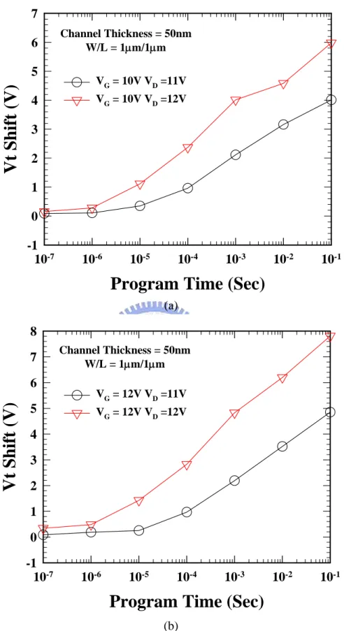
(49) 7 6. Vt Shift (V). 5 4. Channel Thickness = 50nm W/L = 1μm/1μm VG = 10V VD =11V VG = 10V VD =12V. 3 2 1 0 -1 10-7. 10-6. 10-5. 10-4. 10-3. 10-2. 10-1. 10-2. 10-1. Program Time (Sec) (a). 8 7. Vt Shift (V). 6 5. Channel Thickness = 50nm W/L = 1μm/1μm VG = 12V VD =11V VG = 12V VD =12V. 4 3 2 1 0 -1 10-7. 10-6. 10-5. 10-4. 10-3. Program Time (Sec) (b). Fig. 3-8 Program speed characteristic for different programming conditions. This gate length and width are both 1μm, and channel thickness is 50nm. (a) At VG=10V and different VD. (b) At VG=12V and different VD. The programming time can be as short as 10μs if the windows margin is set about 1V with VD=12V. 34.
(50) 5. Vt Shift (V). 4. Channel Thickness = 50nm W/L = 1μm/1μm VG = 10V VD =11V. 3. VG = 12V VD =11V. 2 1 0 -1 10-7. 10-6. 10-5. 10-4. 10-3. 10-2. 10-1. 10-2. 10-1. Program Time (Sec) (a). 8 7. Vt Shift (V). 6 5. Channel Thickness = 50nm W/L = 1μm/1μm VG = 10V VD =12V VG = 12V VD =12V. 4 3 2 1 0 -1 10-7. 10-6. 10-5. 10-4. 10-3. Program Time (Sec) (b) Fig. 3-9 Program speed characteristic of different programming conditions for 1μm gate length and width, and 50nm channel thickness. (a) At VD=11V and different VG. (b) At VD=12V and different VG. When applying the same VD, that VG is increased doesn’t obviously improve program speed. 35.
(51) 8 7. Channel Thickness = 50nm W/L = 0.8μm/0.8μm. Vt Shift (V). 6 5. VG = 10V VD =10V VG = 10V VD =11V. 4 3 2 1 0 -1 10-7. 10-6. 10-5. 10-4. 10-3. 10-2. 10-1. 10-2. 10-1. Program Time (Sec) (a). 9 8. Channel Thickness = 50nm W/L = 0.8μm/0.8μm. Vt Shift (V). 7 6 5. VG = 12V VD =10V VG = 12V VD =11V. 4 3 2 1 0 -1 10-7. 10-6. 10-5. 10-4. 10-3. Program Time (Sec) (b) Fig. 3-10 Program speed characteristic for different programming conditions. This gate length and width are both 0.8μm, and channel thickness is 50nm. (a) At VG=10V and different VD. (b) At VG=12V and different VD. The programming time can be as short as 10μs if the windows margin is set about 1V with VD=11V. 36.
(52) Vt Shift (V). 7 6. Channel Thickness = 50nm W/L = 0.8μm/0.8μm. 5. VG = 10V VD =10V. 4. VG = 12V VD =10V. 3 2 1 0 -1 10-7. 10-6. 10-5. 10-4. 10-3. 10-2. 10-1. 10-2. 10-1. Program Time (Sec) (a). 9 8. Channel Thickness = 50nm W/L = 0.8μm/0.8μm. Vt Shift (V). 7 6 5. VG = 10V VD =11V VG = 12V VD =11V. 4 3 2 1 0 -1 10-7. 10-6. 10-5. 10-4. 10-3. Program Time (Sec) (b) Fig. 3-11 Program speed characteristic of different programming conditions for 0.8μm gate length and width, and 50nm channel thickness. (a) At VD=10V and different VG. (b) At VD=11V and different VG. When applying the same VD, that VG is increased doesn’t obviously improve program speed. 37.
(53) 8 7. Channel Thickness = 100nm W/L = 1μm/1μm. Vt Shift (V). 6 5. VG = 10V VD =10V VG = 10V VD =11V. 4 3 2 1 0 -1 10-7. 10-6. 10-5. 10-4. 10-3. 10-2. 10-1. 10-2. 10-1. Program Time (Sec) (a). 8 7. Vt Shift (V). 6 5. Channel Thickness = 100nm W/L = 1μm/1μm VG = 12V VD =10V VG = 12V VD =11V. 4 3 2 1 0 -1 10-7. 10-6. 10-5. 10-4. 10-3. Program Time (Sec) (b) Fig. 3-12 Program speed characteristic for different programming conditions. This gate length and width are both 1μm, and channel thickness is 100nm. (a) At VG=10V and different VD. (b) At VG=12V and different VD. The programming time can be as short as 10μs if the windows margin is set about 1V with VD=11V. 38.
(54) 7 6. Vt Shift (V). 5 4. Channel Thickness = 100nm W/L = 1μm/1μm VG = 10V VD =10V VG = 12V VD =10V. 3 2 1 0 -1 10-7. 10-6. 10-5. 10-4. 10-3. 10-2. 10-1. 10-2. 10-1. Program Time (Sec) (a). 9 8. Channel Thickness = 100nm W/L = 1μm/1μm. Vt Shift (V). 7 6 5. VG = 10V VD =11V VG = 12V VD =11V. 4 3 2 1 0 -1 10-7. 10-6. 10-5. 10-4. 10-3. Program Time (Sec) (b) Fig. 3-13 Program speed characteristic of different programming conditions for 1μm gate length and width, and 100nm channel thickness. (a) At VD=10V and different VG. (b) At VD=11V and different VG. When applying the same VD, that VG is increased doesn’t obviously improve program speed. 39.
(55) 8 7. Channel Thickness = 100nm W/L = 0.8μm/0.8μm. Vt Shift (V). 6 5. VG = 10V VD =9V VG = 10V VD =10V. 4 3 2 1 0 -1 10-7. 10-6. 10-5. 10-4. 10-3. 10-2. 10-1. 10-2. 10-1. Program Time (Sec) (a). 10 9. Vt Shift (V). 8. Channel Thickness = 100nm W/L = 0.8μm/0.8μm. 7. VG = 12V VD =9V. 6. VG = 12V VD =10V. 5 4 3 2 1 0 -1 10-7. 10-6. 10-5. 10-4. 10-3. Program Time (Sec) (b) Fig. 3-14 Program speed characteristic for different programming conditions. This gate length and width are both 0.8μm, and channel thickness is 100nm. (a) At VG=10V and different VD. (b) At VG=12V and different VD. The programming time can be as short as 10μs if the windows margin is set about 1V with VD=10V. 40.
(56) 7 6. Channel Thickness = 100nm W/L = 0.8μm/0.8μm. Vt Shift (V). 5 4. VG = 10V VD =9V VG = 12V VD =9V. 3 2 1 0 -1 10-7. 10-6. 10-5. 10-4. 10-3. 10-2. 10-1. 10-2. 10-1. Program Time (Sec) (a). 10 9. Vt Shift (V). 8. Channel Thickness = 100nm W/L = 0.8μm/0.8μm. 7. VG = 10V VD =10V. 6. VG = 12V VD =10V. 5 4 3 2 1 0 -1 10-7. 10-6. 10-5. 10-4. 10-3. Program Time (Sec) (b) Fig. 3-15 Program speed characteristic of different programming conditions for 0.8μm gate length and width, and 100nm channel thickness. (a) At VD=9V and different VG. (b) At VD=10V and different VG. When applying the same VD, that VG is increased doesn’t obviously improve program speed. 41.
數據
+7
相關文件
• Each student might start from a somewhat different point of view and experience the encounters with works of art and ideas in a different way... Postmodern
電腦內部是使⽤用位元 (Bit) 這個基本單位來表⽰示資料 並儲存於記憶單元 (記憶體) 或輔助記憶單元 (硬碟) 中。.. 每個位元只可以表⽰示
Two cross pieces at bottom of the stand to make a firm base with stays fixed diagonally to posts. Sliding metal buckles for adjustment of height. Measures accumulated split times.
Type case as pattern matching on values Type safe dynamic value (existential types).. How can we
- Different KLA/subject departments can collaborate and arrange a diversified range of reading activities and schemes for students to gain knowledge across disciplines, and
220V 50 Hz single phase A.C., variable stroke control, electrical components and cabling conformed to the latest B.S.S., earthing through 3 core supply cable.. and 2,300 r.p.m.,
The Hilbert space of an orbifold field theory [6] is decomposed into twisted sectors H g , that are labelled by the conjugacy classes [g] of the orbifold group, in our case
雙極性接面電晶體(bipolar junction transistor, BJT) 場效電晶體(field effect transistor, FET).
