Characterization of phosphorus-doped and boron-doped diamond-like carbon emitter
arrays
Chia-Lun Tsai, Chia-Fu Chen, and Chien-Liang Lin
Citation: Journal of Applied Physics 90, 4847 (2001); doi: 10.1063/1.1408587
View online: http://dx.doi.org/10.1063/1.1408587
View Table of Contents: http://scitation.aip.org/content/aip/journal/jap/90/9?ver=pdfcov Published by the AIP Publishing
Articles you may be interested in
Fabrication of triode diamond field emitter arrays on glass substrate by anisotropic conductive film bonding J. Vac. Sci. Technol. B 19, 954 (2001); 10.1116/1.1361039
Estimation of emission field and emission site of boron-doped diamond thin-film field emitters J. Vac. Sci. Technol. B 18, 1018 (2000); 10.1116/1.591318
Electron emission performance of nitrogen-doped hydrogen-free diamond-like carbon coating on Mo-Tip field emitter arrays
J. Vac. Sci. Technol. B 18, 933 (2000); 10.1116/1.591301
Properties of plasma enhanced chemical vapor deposition diamond-like carbon films as field electron emitters prepared in different regimes
J. Vac. Sci. Technol. B 17, 679 (1999); 10.1116/1.590617
Emission stability of a diamond-like carbon coated metal-tip field emitter array J. Vac. Sci. Technol. B 17, 486 (1999); 10.1116/1.590581
Characterization of phosphorus-doped and boron-doped diamond-like
carbon emitter arrays
Chia-Lun Tsai,a)Chia-Fu Chen, and Chien-Liang Lin
Department of Materials Science and Engineering, National Chiao Tung University, 1001 Ta Hsueh Road, Hsinchu 30050, Taiwan, Republic of China
共Received 30 April 2001; accepted for publication 10 August 2001兲
We synthesized phosphorus-doped and boron-doped emitters by using trimethylphosphite P共OCH3兲3
and trimethylborate B共OCH3兲3as doping sources in a microwave plasma chemical vapor deposition
system. Based on our experimental results from scanning electron microscopy and Raman spectra, there is much difference among undoped, phosphorus-doped, and boron-doped diamondlike material. In addition, doping both phosphorus and boron can enhance electric properties by reducing the turn-on voltage and can increase the emission current density. The turn-on voltages of undoped, boron-doped, and phosphorus-doped emitters in triode-type field emitter arrays are 15, 8, and 5 V, respectively. The emission currents of boron-doped and phosphorus-doped emitters are about 20 and 80 times larger than the undoped. © 2001 American Institute of Physics.
关DOI: 10.1063/1.1408587兴
I. INTRODUCTION
Diamond and diamond-like carbon共DLC兲 are presently being investigated and applied for use in field emission de-vices because diamond has negative electron affinity and ro-bust mechanical and chemical properties. The diamond growth process used by researchers to make the devices also varies greatly. Observations of electron emission from chemical vapor deposition 共CVD兲 diamond under relative low electric fields共3–40 V/m兲 have been reported.1–3 Fab-rication of diamond field emitter arrays has also been attempted4 and a diode-structured prototype field emission display based on a diamond-like carbon cathode has been demonstrated.5However, it is not entirely clear how the elec-tron emission from these seemingly undoped or p-typed-doped CVD diamonds can occur at such low fields.
Usually, for a semiconductor field emitter, the emitter electrons can originate from either the conduction band, the valence band, and/or surface states. Diamond has a wide band gap with Eg⫽5.5 eV. In order to induce stable electron field emission from diamond, either the bulk or the surface must first be made conductive. It is believed that the impu-rities such as nitrogen, boron or phosphorus can enhance diamond’s electron property by offering holes or electrons.
II. EXPERIMENT
A similar fabrication process for this metal-insulator-semiconductor 共MIS兲 diode and diamond deposition proce-dure has been previously presented.6 In this work, first we designed the MIS diode structure and fabricated the MIS diode by semiconductor process technologies. Figure 1 dis-plays the procedure of the MIS diode and Fig. 2 shows the photographs of MIS diode structure. After fabricating the MIS diode, we put it in the bias assisted microwave plasma chemical vapor deposition system to deposit diamond-like
emitters. The reactive gases used in deposition were the con-ventional mixture of CH4–H2 with trimethylphosphite
P共OCH3兲3 and trimethylborate B共OCH3兲3 as the doping
sources. All the experiments of the diamond deposition used two-step depositions. The first step is employed as a nucle-ation process: the flow rates of CH4/H2and deposition time remain constant at 10/200 sccm and 30 min, respectively. The second step is the growth process and the total deposi-tion normally lasts for 60 min. While processing, the speci-mens were subjected to a negative bias voltage of 130 V. Table I lists the experimental conditions. After processing, the CVD material was to characterize the quality of the dia-mond material.
III. RESULTS AND DISCUSSION A. SEM analysis
For the undoped emitters, the diamond nuclei are not observed when the negative bias voltage is below 80 V. Fur-thermore, the bias voltage of 90–100 V only grows tiny tips inside the hole. The higher bias voltage we apply, the more emitters we can obtain. This implies that the higher bias voltage enhances the growth of the emitters. Once we in-crease the bias voltage over 150 V, diamond was not only inside the hole but also on the Pt gate. Indeed, the diamond may replace the Pt to form the diamond-gated field emissions arrays共FEAs兲. In the worst case scenario, this phenomenon will taint the I – V measurement because the field emission current may be inexact because of the influence from both the diamond-like nano emitters and diamond-like-gated sur-face. In this article, the negative bias voltage⫽130 V is used. Figures 3 and 4 display scanning electron microscopy共SEM兲 photographs of the undoped diamond emitters. Undoped dia-mond emitters have several branches on their lateral or top directions. But from Figs. 5 and 6, the doping ones only have tiny tips around them. The most significant phenomenon is the quantity of diamond emitters. Undoped diamond emitters
a兲Electronic mail: [email protected]
4847
0021-8979/2001/90(9)/4847/5/$18.00 © 2001 American Institute of Physics
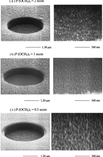
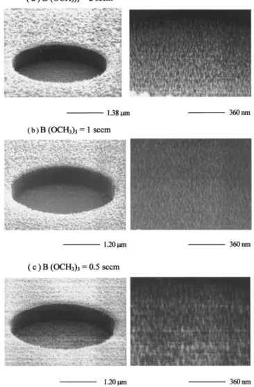
have higher growth rate than doping ones. The lower growth rate of the doped emitters could be explained by the follow-ing points. 共I兲 P共OCH3兲3 or B共OCH3兲3 is a CH3-rich
com-pound that decomposes in plasma to produce an equal quan-tity of CH3 radicals to balance the carbon source in the gas
phase, thus the deposition rate will be reduced due to the increase of etching rate. 共II兲 The lower growth rate of the doped samples is most likely due to the oxygen content con-tained in the P共OCH3兲3or B共OCH3兲3. There were more
oxy-gen atoms than phosphorus atoms in the doping source, which may be related to the etching of nondiamond carbon from the growing surface resulting in a lower growth rate. FIG. 1. Fabricated procedure of diamond emitters on the FEAs with gated
diode pattern.
FIG. 2. The SEM photograph of MIS diode structure with 50⫻50 circles.
TABLE I. Deposition conditions.
Sample
First step flow rate CH4/H2⫹doping source
共sccm兲
Second step flow rate CH4/H2⫹doping source 共sccm兲 A共undoped兲 10/200 7.5/200 B共undoped兲 10/200 5/200 C共undoped兲 10/200 2/200 D共phosphorus doped兲 10/200⫹2 2/200⫹2 E共phosphorus doped兲 10/200⫹1 2/200⫹1 F共phosphorus doped兲 10/200⫹0.5 2/200⫹0.5 G共Boron doped兲 10/200⫹2 2/200⫹2 H共Boron doped兲 10/200⫹1 2/200⫹1 I共Boron doped兲 10/200⫹0.5 2/200⫹0.5 First step deposition time⫽30 min Second step deposition time⫽30 min, Bias voltage⫽⫺130 V Total pressure⫽2 KPa
MW power⫽300 W Substrate temp.共°C兲⫽⬃660
Doping source: P共OCH3兲3 andB共OCH3兲3
FIG. 3. The SEM photograph of undoped diamond emitters.
4848 J. Appl. Phys., Vol. 90, No. 9, 1 November 2001 Tsaiet al.
The same effects may also occur when adding O2 to the
CH4–CO2 gas mixture. 7
Additionally, many investigations have confirmed that phosphorus will lower the diamond growth rate in H2–CH4mixtures.
7,8
B. Raman spectra
The microstructure and quality of the amorphous diamond-like carbon films were determined by Raman spec-tra. Raman measurements were performed at 514.5 nm at 1 cm⫺1resolution, integration times were 1 min at 30 mW Ar ion laser power. Figure 7 gives the Raman spectrum of un-doped diamond emitters. We can see there are two obvious peaks located around 1350 cm⫺1共D band兲 and 1580 cm⫺1共G band兲. Normally a sharp peak at 1332 cm⫺1corresponding to the diamond zone center phonon line would be the principle
Raman active feature in high quality crystalline CVD mate-rial. In this work, the spectral feature is diminished by stron-ger phonon bands attributable to diamond-like carbon 共D band兲 and crystalline graphite 共G band兲. This implies that the undoped emitters contain more graphitic material than dia-mond, and should strictly be classified as a diamond-like carbon 共DLC兲 material. Figures 8 and 9 indicate that the graphitic content becomes even more dominant in the emitter material as the doping level of boron or phosphorus is in-creased. This observation is borne out by the fact that both doping gases are methyl-rich compounds. Thus, the etching rate declined while the quantity of amorphous carbon or graphite increased in the resultant films. A Raman shift oc-curs because of the internal stress in the diamond. This stress could be attributed to the following reasons: 共I兲 the lattice mismatch between the diamond and phosphorus during growth; and 共II兲 the thermal expansion coefficients of the diamond and substrate as well as the nanocrystalline nature of the diamond.
C.I – V measurement
Although diamond and DLC films have stable electron emissions at the low field, the nature of electron emission
FIG. 4. The SEM photograph of undoped diamond emitters with various methane concentration共a兲 sample A, 共b兲 sample B, and 共c兲 sample C.
FIG. 5. The SEM photograph of phosphorus-doped diamond emitters with various doping concentration 共a兲 2 sccm, 共b兲 1 sccm and 共c兲 0.5 sccm, respectively.
from these materials remains unclear.9We are currently em-ploying different approaches to explain the ultralow emission fields. Many factors affect the field emission characterization of diamond including impurity, and defect levels10 in the diamond band gap; hot electron transport in interfaced
structures;11grain boundary effects;12and geometric field en-hancement 共兲 by morphology protrusions or narrow con-ductive grain boundaries between insulating grains. In this article, there are significant differences between phosphorus and boron doping. Figure 10 shows the field emission current density (Je) of undoped; boron-doped, and phosphorus-doped diamond-like emitters with 0.013, 0.24, and 1.03 A/cm2. The currents of boron-doped and phosphorus-doped emitters are 20 and 80 times larger than the undoped one. The electron emitting properties were further evaluated by the Fowler–Nordheim plot shown as an inset to Fig. 10.
The experimental results confirm that phosphorus-doped emitters have a better field emission property than boron doped for the following reasons. Doping with phosphorus has substantially more influence on conductivity than doping with boron. The other is due to the morphology of the emit-ters’ structure. Phosphorus also provides its conduction elec-trons with more opportunity to be extracted because ionized donors form a space charge layer.13Solid-state physics indi-cates that doping boron or phosphorus will instigate an en-ergy band modification in the material by generating a donor or acceptor level that provides more electrons or holes for the
FIG. 6. The SEM photograph of boron-doped diamond emitters with vari-ous doping concentration共a兲 2 sccm, 共b兲 1 sccm, and 共c兲 0.5 sccm, respec-tively.
FIG. 7. The Raman spectrum of samples A, B, C grown at different methane concentration.
FIG. 8. The Raman spectrum of samples D, E, F grown at different phos-phorus concentration.
FIG. 9. The Raman spectrum of samples G, H, I grown at different boron concentration.
4850 J. Appl. Phys., Vol. 90, No. 9, 1 November 2001 Tsaiet al.
material. These increase the total conductivity and net flux of carriers.
The field emission property of diamond can be enhanced by increasing the s p2 content because of the following
rea-sons:
共I兲 The defect-induced band created by the sp2 content.
The defect-induced energy band created by the s p2 con-tent is responsible for the field emission enhancement. A defect-induced energy band can be induced throughout the diamond energy gap in response to the presence of a wild variety of structural defects created as a consequence of the
s p2 particles. The formation of these defect bands raises the Fermi level toward the conduction band, and thus reduces the work function for enhancing field emission.
共II兲 The field enhancement factor is increased by the
s p2-diamond-s p2 microstructures.
Conducting s p2 particles in isolated diamond form cas-caded s p2-diamond-s p2metal-insulator-metal共MIM兲 micro-structures which could enhance the field enhancement factor. The field enhancement factor is affected by the following geometrical parameters of the device structure: the gate opening diameter, tip radius, emitter high, and tip position with respect to the center of the gate thickness and the emit-ter morphology. Adding phosphorus or boron changes their structures and also affects the field enhancement factor.
IV. CONCLUSIONS
In this article, we synthesized phosphorus-doped and boron-doped emitters by using trimethylphosphite P共OCH3兲3
and trimethylborate B共OCH3兲3 as doping sources. Undoped emitters have higher growth rate than doping ones. The lower growth rate of the doped emitters could be explained by the following points. 共I兲 P共OCH3兲3 or B共OCH3兲3 is a
CH3-rich compound that decomposes in plasma to produce
an equal quantity of CH3 radicals to balance the carbon
source in the gas phase, thus the deposition rate will be re-duced due to the increase of etching rate. 共II兲 The lower growth rate of the doped samples is most likely due to the oxygen content contained in the P共OCH3兲3 or B共OCH3兲3. Doping both phosphorus and boron can enhance electric properties by reducing the turn-on voltage and can increase the emission current density. The emission current densities of boron-doped and phosphorus-doped emitters are about 20 and 80 times larger than the undoped.
1
M. W. Geis, N. N. Efremow, J. D. Woodhouse, M. D. McAleese, M. Marchywka, D. G. Socker, and J. F. Hochedez, IEEE Electron Device Lett. 12, 456共1991兲.
2C. Wang, A. Garcia, D. C. Ingram, M. Lake, and M. E. Kordesch,
Elec-tron. Lett. 27, 1459共1991兲.
3
N. S. Xu, Y. Tzeng, and R. V. Latham, J. Phys. D 26, 1776共1993兲.
4
K. Okano, K. Hoshina, M. Iida, S. Koizumi, and T. Inuzuka, Appl. Phys. Lett. 64, 2742共1994兲.
5H. K. Schmidt, M. H. Clark. I. Yee, and N. Kumar, Abstract for the SID
Manuf. Conference, 1994, p. 21.
6C. F. Chen, H. C. Wang, and H. C. Hsieh, Jpn. J. Appl. Phys. 39, 1880
共2000兲.
7C. F. Chen, T. M. Hang, and S. H. Cheng, J. Appl. Phys. 74, 4483共1993兲. 8S. N. Schauer, J. R. Flemish, and R. Wittstruck, Appl. Phys. Lett. 64, 1094
共1994兲.
9J. Ristein, Diamond Relat. Mater. 9, 1129共2000兲.
10W. Zhu and G. P. Kochanski, Mater. Res. Soc. Symp. Proc. 416, 443
共1996兲.
11N. M. Miskovsky, P. H. Cutler, Z.-H. Huang, P. D’Ambrosio, and P.
Lerner, Mater. Res. Soc. Symp. Proc. 416, 437共1996兲.
12A. V. Karabutov, V. D. Frolov, S. M. Pimenov, and V. I. Konov, Diamond
Relat. Mater. 8, 763共1999兲.
13
K. Kuriyama, C. Kimura, S. Koizumi, M. Kamo, and T. Sugino, J. Vac. Sci. Technol. B 17, 723共1999兲.
FIG. 10. The Je– V curve of undoped, phosphorus-doped, and boron-doped diamond emitters and an inset of Fowler–Nordheim plot.