國 立 交 通 大 學
電子工程學系 電子研究所碩士班
碩士論文
90 奈米混合臨界電壓標準元件庫
設計及特性化
90nm Mixed-Threshold Voltage Standard Cell
Library Design and Characterization
指導教授:周 世 傑 博士
研 究 生:林 俊 誼
90 奈米混合臨界電壓標準元件庫
設計及特性化
90nm Mixed-Threshold Voltage Standard Cell
Library Design and Characterization
研究生:林俊誼 Student: Jyun-Yi Lin
指導教授:周世傑 Advisor: Dr.
Shyh-Jye Jou
國 立 交 通 大 學
電子工程學系 電子研究所碩士班
碩士論文
A Thesis
Submitted to Department of Electronics Engineering & Institute of Electronics College of Electrical and Computer Engineering
National Chiao Tung University in Partial Fulfillment of the Requirements
for the Degree of Master In
Electronics Engineering October 2007
Hsinchu, Taiwan, Republic of China
90 奈米混合臨界電壓標準元件庫設計及特性化
學生: 林俊誼 指導教授: 周世傑
國立交通大學
電子工程學系 電子研究所碩士班
摘要
摘要
摘要
摘要
隨著製程的進步以及各種攜帶型電子產品需求的增加,功率消耗對於這些產 品變得相當的重要,例如:使用太陽能電池的助聽器 、新型手機…等。在本篇 論文中,我們提出首先介紹關於深次微米 CMOS 標準元件庫的時脈效能和能量 特性化流程的概論。接著我們提出一種在電路中使用混合臨界電壓電晶體的方式 來取代單一臨界電壓電晶體的方式,使電路能夠在不犧牲速度的情況下,達到低 功率的效果。我們找出在拉升及拉降結構中延遲時間的關鍵路徑,以及關鍵路徑 中最長延遲時間的關鍵電晶體。接著我們將關鍵電晶體置換成較低臨界電壓的電 晶體,並且重新調整較低臨界電壓的電晶體尺寸,使新電路的速度能與原本的電 路接近。利用這種方式,我們不需要增加額外的電路,也不需要更改電路架構, 即可達到低功率的需求。此外大部分電晶體路徑中的漏電流將會被阻擋住。 我們利用這種混合臨界電壓的方式來建立 90 奈米低功率標準元件庫。接著 利用這個低功率標準元件庫來合成電路並且和高臨界電壓標準元件庫的效能比 較。我們的混合臨界電壓標準元件庫在動態功率消耗上可以節省 5%到 30%,在 延遲時間功率乘積上可以節省 20%到 55%,而在面積方面因為佈局規則的限制, 增加了 0%到 40%。90nm Mixed-Threshold Voltage Standard Cell Library
Design and Characterization
Student: Jyun-Yi Lin Advisor: Dr.
Shyh-Jye Jou
Department of Electronics Engineering
Institute of Electronics
National Chiao Tung University
Abstract
With the advance of process technology and the increasing requirement of portable electric products, the power consumption of these products becomes very important. In this thesis, we first make the overview about the advanced characterization flow of timing and power in deep submicron CMOS standard cell library. Then, we propose a methodology using mixed-threshold voltage transistors in a circuit instead of single normal-threshold voltage transistors to reduce power consumption with the same timing performance. We find out the critical path and the critical transistors on the critical path that result in the longest delay time in the pull-up and pull-down networks, respectively. Then we replace the critical transistors with lower threshold voltage transistors and do resizing to meet the time performance of original circuits. Using this technique, we do not have to use additional transistors and do not change the structure of circuits to obtain the requirement of low power. Moreover, the leakage current is also blocked in most of the transistor paths.
We apply this mixed-threshold voltage methodology to establish our 90nm low power standard cell library. Then we use many design examples to compare the performance with the high-Vt standard cell library and make the conclusion that we can have around 5% to 30% dynamic power saving, 20% to 55% delay-power product saving and the area is 0% to 40% larger than the standard cells with single high-Vt transistors.
誌謝
本論文的完成,首先謝周世傑教授用心指導及修改,經由一次又
一次與老師的討論中,獲得許多寶貴的經驗。藉由經驗的累積,讓我
在研究的過程愈來愈順利。感謝劉建男老師、黃俊達老師、陳繼展經
理在口試時給我的指導與建議,讓我的論文能夠更加完備,口試委員
們詳盡的意見,補足我思慮不周之處。
除了老師之外,同學及朋友們在精神上給予我很大的鼓勵,周
group 的學長姐們,林志憲學長、林育群學長、陳筱筠學姐、王儷蓉
學姐、胡嘉琳學姐、魏庭楨學長、朱昌敏學長、莊誌華學長、劉瑋昌
學長、嚴紹維學長,在我研究遇到問題時,大力提供幫助。SPICE、
阿樸、俊男、國光、晉欽、建君、小 VAN、篤雄、JUJU、秀逗、怡秀
以及各位同學及朋友,有你們的陪伴幫助,讓我在兩年研究生活過得
很充實,不論將來各自如何發展,我們的友誼長存。
最後,我想將完成碩士學位的光榮獻給我的家人,感謝他們的教
誨及信任,無悔的付出讓我能夠沒有後顧之憂,盡全力發揮。
林俊誼
謹誌於 新竹
2007 十月
Contents
Chapter 1 Introduction ... 1
1.1 Introduction of Standard Cell Library ... 1
1.2 Deep-submicron Circuit Design Issues ... 2
1.3 Motivation and Goals ... 3
1.4 Thesis Organization ... 4
Chapter 2 Background Overview ... 6
2.1 Power Dissipation in CMOS circuits ... 6
2.1.1 Dynamic Power Dissipation ... 6
2.1.2 Static Power Dissipation ... 7
2.2 Common Formats of Standard Cell Library ... 10
2.3 Brief Introduction to Liberty File ... 11
2.3.1 Classification of Power [4] [5] ... 14
2.3.2 Classification of Time ... 18
2.3.3 Create Look-up Table ... 20
2.4 Design of Standard Cell Library ... 22
2.5 Summary ... 23
Chapter 3 Timing and Power Model Characterization Flow ... 24
3.1 Timing Characterization Flow ... 24
3.1.1 Transition Time and Propagation Delay time ... 24
3.1.2 Input Capacitance ... 28
3.2 Power Characterization Flow ... 29
3.2.1 Internal Power ... 29
3.2.2 Leakage Power ... 30
3.3 Summary ... 31
Chapter 4 Low Power Standard Cell Library ... 32
4.1 Overview of Low Power Standard Cell Design Methodology ... 32
4.1.1 Multiple Threshold Voltage Circuit ... 33
4.1.2 Multiple Supply Voltage ... 40
4.2 Standard Cell Selection Rule ... 42
4.3 Low Power Standard Cell Library Design Flow ... 45
4.4.1 INV ... 57
4.4.2 3-input NAND and AOI31 ... 58
4.4.3 1-bit Half Adder ... 61
4.4.4 DFF and SETDFF ... 62
4.5 Summary ... 65
Chapter 5 Design Examples by Low Power Standard Cell Library ... 66
5.1 C17 ... 66
5.2 32 bit Ripple Adder ... 67
5.3 32-bit Wallace Tree Multiplier ... 68
5.4 32-bit Shift Register ... 70
Chapter 6 Conclusions ... 72
Reference ... 73
List of Figures
Fig. 1.1 Cell-based design flow ... 2
Fig. 2.1 Switching power example ... 7
Fig. 2.2 Static CMOS leakage sources... 8
Fig. 2.3 Example of .lib file ... 13
Fig. 2.4 2-Input NOR gate ... 17
Fig. 2.5 Transition time and propagation delay time ... 18
Fig. 2.6 Non-Linear Delay Model (NLDM) example ... 19
Fig. 2.7 Example of lookup table of the propagation delay time ... 21
Fig. 2.8 Example of using lookup table ... 21
Fig. 2.9 The design flow of creating a standard cell library [5] ... 23
Fig. 3.1 (a) Power vs. input transition time (b) Delay_rise vs. input transition ... 26
Fig. 3.2 3-input NAND schematic ... 27
Fig. 3.3 Circuit diagram of creating capacitance vs. delay time look up table ... 29
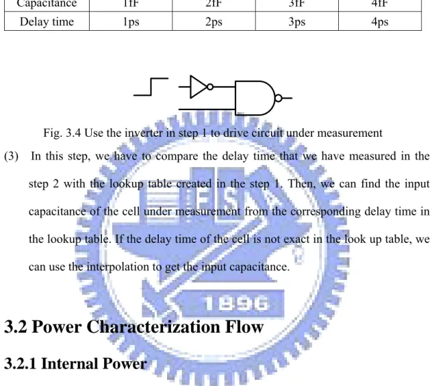
Fig. 3.4 Use the inverter in step 1 to drive circuit under measurement ... 29
Fig. 3.5 Example of input dependent leakage power format ... 31
Fig. 4.1 Schematic of MTCMOS circuits (a) Original MTCMOS (b) PMOS insertion MTCMOS and (c) NMOS insertion MTCMOS ... 34
Fig. 4.2 Schematic of SCCMOS circuits (a) PMOS insertion SCCMOS ... 35
Fig. 4.3 Dual-threshold CMOS circuit [1] ... 37
Fig. 4.4 MVT schemes of [10] (a) MVT1 scheme and (b) MVT2 scheme ... 38
Fig. 4.5 MVT schemes of[12] (a) MVT-NAND2 and (b) MLVT-NAND2 ... 39
Fig. 4.6 Schematic of DTMOS inverter ... 40
Fig. 4.7 Example of level converter ... 41
Fig. 4.9 The block diagram of CVS ... 41
Fig. 4.10 The block diagram of CFMV ... 42
Fig. 4.11 Numbers of pitch for BUF with driving ability X5 (a) BUFX2+BUFX3 (b) BUFX5 ... 44
Fig. 4.12 NMOS saturation current with different threshold voltage and channel ... 46
Fig. 4.13 PMOS saturation current with different threshold voltage and channel ... 47
Fig. 4.14 The timing waveforms of the inverter gates ... 48
Fig. 4.15 Diffusion region geometry ... 49
Fig. 4.16 Circuit simulation environment with capacitance load ... 53
Fig. 4.17 Fixed output load capacitance and sweep input transition time of ... 54
Fig. 4.18 Fixed input transition time and sweep output load capacitance (a) Power vs. output load capacitance(b) Delay_rise vs. output load ... 56
Fig. 4.19 Circuit simulation environment with FO4 load ... 56
Fig. 4.20 Inverter gate (A) HVT and (B) MVT ... 57
Fig. 4.21 Schematic of 3-input NAND gate ... 59
Fig. 4.22 Schematic of AOI31 gate ... 60
Fig. 4.23 (a) Block diagram of 1-bit Half Adder (b) Mixed-Vt 1-bit Half Adder schematic ... 61
Fig. 4.24 Mixed-Vt DFF schematic ... 63
Fig. 4.25 Mixed-Vt SETDFF schematic ... 63
List of Tables
Table 2.1 The lookup table of 2-input NAND ... 22
Table 3.1 Truth table of 3-input NAND ... 27
Table 3.2 Capacitance vs. Delay table ... 29
Table 3.3 Leakage power of a 2-input NOR gate ... 30
Table 4.1 Logical effort of frequently used gates [6] ... 43
Table 4.2 90nm Leakage current with normal-Vt and low-Vt Table 4.3 Inverter gate with high-Vt, mixed-Vt and normal-Vt ... 51
Table 4.4 Time and power table of INV with VDD=0.5 V ... 57
Table 4.5 Time and power of 3 statges inverter driving 100 fF with VDD=0.5 V ... 58
Table 4.6 Time and power table of 3-input NAND with VDD=0.5 V ... 59
Table 4.7 Leakage power of 3-input NAND at all the input combinations, unit: pW . 59 Table 4.8 Power and leakage power of AOI31 with VDD=0.5 V ... 60
Table 4.9 Time and power table of 1-bit half adder with VDD=0.5 V ... 62
Table 4.10 Leakage power table of 1-bit half adder ... 62
Table 4.11(a) Time and power table of Mixed-Vt DFF with VDD=0.5 V ... 64
Table 4.11(b) Time and power table of Mixed-Vt DFF with VDD=1 V ... 64
Table 4.12(a) Time and power table of Mixed-Vt SETDFF with VDD=0.5 V ... 64
Table 4.12(b) Time and power table of Mixed-Vt SETDFF with VDD=1 V ... 64
Table 5.1 Time and power table of C17 circuit with VDD=0.6 v ... 67
Table 5.2(a) Synthesis result of 32bit ripple adder with VDD=1 v ... 68
Table 5.2(b) Synthesis result of 32bit ripple adder with VDD=0.6 v ... 68
Table 5.3(a) Synthesis result of 32 bit wallace tree multiplier with VDD=1 v ... 69
Table 5.3(b) Synthesis result of 32 bit wallace tree multiplier with VDD=0.6 v ... 70
Table 5.4(b) Synthesis result of 32 bit shift register with VDD=0.6 v ... 71
1
Chapter 1
Introduction
1.1 Introduction of Standard Cell Library
With the novel process technology is going to deep-submicron generation, the high integrated and high complex system on chip (SOC) design methodology becomes practical and popular. When circuit designers would like to use the cell-based design flow to design a digital chip, they have to ensure its specifications such as the timing performance, power consumption, area…etc of the chip could meet the requests of the circuit. A typical cell-based design flow is shown in Fig. 1.1. For timing specification, most designers and the synthesis tools use the method of static timing analysis (STA) to verify their timing performance. If the timing performance doesn’t meet the specification, circuit designers or synthesis tools will replace some cells in the circuit or change the architecture of the circuit to improve the timing performance. Then, they would reiterate above steps until the timing performance meets the specification. The methods to meet the design performance of power and area are like that of timing tuning process. After verifying the characteristics of the chip meets the specification, designers have to use an automatic placement and routing tool to draw the circuit layout in order to tape out the chip.
2
from circuit synthesis step to automatic place and route step. The synthesis tool can implement a large circuit with the cells supplied by the cell library. The standard cell library also supplies the timing, power, and area information of cells to let the synthesis tool optimize the circuit design to meet the specifications.
Fig. 1.1 Cell-based design flow
1.2 Deep-submicron Circuit Design Issues
As the novel technology process progress, the total power dissipation is not only determined by the switching power and the internal power dissipation but also the leakage power dissipation. When the transistor size scales down, the supply voltage has to be scaled down at the same time in order to save power and considers the
3
problem of device reliability. With the decreasing of the supply voltage, the threshold voltage has to be scaled down to meet the performance requirements. However, low threshold voltage will increase the sub-threshold leakage current and it will dominate the total leakage power at 90nm and below deep-submicron technology processes. In 90nm process, the threshold voltage between 0.1V and 0.2V causes l0nA-order sub-threshold leakage current per logic gate in a standby mode, which leads to l0mA standby current for 1M-gate VLSIs [9]. Therefore, we have to reduce the leakage power very carefully when we design low power circuits at the deep submicron process.
1.3 Motivation and Goals
Many commercial standard cell libraries have been proposed. In the cell base design flow, we can synthesize our design by using the standard cell libraries supported by the foundry factory. However, we can not modify the data in the commercial cell libraries to improve the circuit performance for special design requirement. Therefore, we would like to build a procedure to create a low power standard cell library. With this procedure, we can add some properties that we need in the library to meet our research requirement. For example, if we design a new D-type flip flop or Latch, we can add these new cells in our standard cell library for others to use at any time.
Furthermore, with the growing use of solar batteries, portable and wireless electronic systems, the designer has to reduce the power consumption in the novel VLSI circuit and system designs [1]. Thus, we would like to use low power design technique in our standard cells in order to create a low power standard cell library. There are many methodologies and architectures for low power circuit design. We
4
choose the low power design methodology on circuit and logic level in our low power cell library. In order to reduce the loading of the designer to design a low power circuit such as finding the critical path of the circuit、designing additional circuits used in the standby mode, etc, we want to create low power cells without changing the schematics of cells. Therefore, we would use one of low power design methodologies of multiple threshold voltage (Vt), mixed-Vt, in a cell by replacing the MOSs on the critical path and resizing them to establish our low power standard cell library. Besides, in order to avoid the over design causing the waste of area and power, we characterize this mixed-Vt low power standard cell library by the advanced characterization tool, Parex. Finally, we use our mixed-Vt low power standard cell library to synthesize several design examples and compare the timing and power performance with the single high-Vt standard cell library to demonstrate that our mixed-Vt method is very effective.
1.4 Thesis Organization
In this thesis, a design flow and methodology of Mixed-Vt 90nm CMOS standard cell library is presented. Design and implementation results are demonstrated to show the performance of the proposed mixed-Vt cell library. The thesis organization is described as follows:
Chapter 2 introduces power dissipation of CMOS circuits and the basics of a standard cell library. We will also overview the improvement of present standard cell library in advanced technology.
The characterization flows of time and power in a standard cell library are demonstrated in Chapter 3.
5
Based on present commercial standard cell library, we will show the proposed mixed-Vt low power standard cell library. We will also propose the methodology of low power cell design and establish the flow of setting up the low power standard cell library.
Finally, we use several design examples to demonstrate our low power standard cell library in Chapter 5 and a conclusion is made in Chapter 6.
6
Chapter 2
Background Overview
2.1 Power Dissipation in CMOS circuits
We know that the power consumption of CMOS circuits is composed of two components, the dynamic power and the static power. The power dissipation can be expressed as:
static dynamic
total
P
P
P
=
+
(2.1)where Ptotal is the total power dissipation, Pdynamic is the dynamic power and Pstatic is the
static power dissipation.
2.1.1 Dynamic Power Dissipation
Dynamic power consumption occurs when the input signal transition results in the signal state transient in the output. At this time, the power that the circuit exhausts is called dynamic power consumption. The following equation shows the power dissipation components of dynamic power.
circuit short internal switching dynamic
P
P
P
P
=
+
+
− (2.2)7
where Pdynamic is the dynamic power, Pswitching is the switching power, Pinternal is the
internal power and Pshort-circuit is the short circuit power dissipation.
For dynamic power consumption, there are three components. One is the power in using to charge or discharge the output (Pswitching) and the parasitic capacitance
(Pinternal)(see Fig. 2.1). The other is short circuit power (see Fig. 2.1) due to the
non-zero rise and fall time of input waveforms. This situation will cause the N/PMOS conducting simultaneously when input signal transits and the current will flow from VDD into ground. In the high speed circuit, the amount of short-circuit power can be ignored due to the fast transition time. The last one is the internal power component. It results from the power supply charges/discharges the internal parasitic capacitance. In Out Switching current Short circuit current Fig. 2.1 Switching power example
2.1.2 Static Power Dissipation
The static power of a CMOS circuit is determined by the leakage current through each transistor. It can be expressed as:
DD static
static
I
V
P
=
⋅
(2.3)Let us take the static CMOS inverter shown in Fig. 2. for instance. When the input signal is at the static state, a continuous high or low voltage level, one MOS of
8
the inverter will be always turn on and the other one will be always turn off. So we can realize that there will be no switching current at this time in the ideal situation. But the secondary effects of leakage current we ignored before becomes more and more significant in the deep submicron process. The leakage sources for the static CMOS circuits are illustrated in Fig. 2.2. These secondary effects including the sub-threshold leakage, the PN reverse bias junction leakage, the Gate Induced Drain Leakage (GIDL) and the punch-through gate oxide tunneling cause small static current flowing through the turned off transistor. These leakage currents will produce power consumption called leakage power. These static currents were ignored in the 0.18μm or the earlier process but they will occupy more portions of the total power consumption in the 90nm and below process.
Fig. 2.2 Static CMOS leakage sources
Designers have to consider many low power design methods to diminish leakage power for low power circuits.
Before introducing the low power design methods, we have to know that what the leakage sources of the MOS are and the reason cause these leakage currents. The leakage sources of the static CMOS circuits in deep submicron process are illustrated
9
in Fig. 2. and we will introduce them respectively. − PN reverse bias diode junction leakage
It is due to the minority carrier drift near the edge of the depletion region and the electron-hole pair generation in the depletion region. It is very small and can be ignored. When the electric field across a reverse-biased p-n junction is continuously high, significant current flow can occur due to band-to-band tunneling. The PN reverse bias diode junction leakage current is about 0.1nA with 1 V reverse bias voltage and 75℃ [19].
− Gate Induced Drain Leakage (GIDL)
It occurs at negative VG and high VD. Where VG is the voltage applied to the gate of a transistor and VD is the voltage applied to the drain of a transistor. It is due to the high electric field under the gate and drain overlap region, which results in the band-to-band tunneling [1-2]. The gate induced drain leakage (GIDL) is about 1nA with VG= -1 V, VD=1.5 V, physical gate width is 1μm and gate length is 100 nm [18].
− Sub-threshold leakage
It is the weak inversion current between source and drain of MOS transistor when the gate voltage is less than the threshold voltage. It increases exponentially with the reduction of the threshold voltage. So it is the critical for low voltage low power (LVLP) CMOS circuit design. The short channel effect (SCE), such as Vth roll-off and Drain-Induced-Barrier-Lowering (DIBL), make the sub-threshold leakage even worse. The sub-threshold leakage current is about 5nA with VGS= 0.5 V, gate width = 1μm and gate length= 90nm in 90nm process [17]. Where VGS is the gate related to source voltage of a transistor. − Punch-through
10
regions approach each other. In the punch-through condition, the gate totally loses the control of the channel current and the sub-threshold slope starts to degrade.
− Gate Oxide Tunneling
It is due to the high electric filed in the gate oxide, includes Fowler-Nordheim tunneling through the oxide band and the direct tunneling through the gate. Fowler-Nordheim tunneling is negligible for the normal device operations, but the direct tunneling is important when the oxide thickness is less than 23nm [1-2]. The gate oxide tunneling current is about 1nA with VGS= 1 V, gate width = 10μm and gate length= 10um in 90nm process [17]. Where VGS is the gate related to source voltage of a transistor.
2.2 Common Formats of Standard Cell Library
Currently, there are two different kinds of standard cell library. The first type is called Advanced Library Format (ALF) [3], and the second type is called Liberty (.lib) [4]. ALF is an IEEE standard 1603-2003. It is a modeling language for library elements used in IC technology. The content of ALF are electrical, functional, and physical models of technology-specific libraries for cell-based and block-based design in a formal language suitable for electronic design automation (EDA) application tools targeted for design and analysis of an IC [3].
Liberty is proposed by Synopsys Corporation. It is the most popular library format in the cell-based design flow now. The main difference between Liberty and ALF is the ranges that they can model. ALF can describe many kinds of characterizations from functional model to physical model. But Liberty is only focusing on the model of timing, power, and signal integrity. We will introduce Liberty more detailed in the following sections.
11
2.3 Brief Introduction to Liberty File
There are some basic attributes declared in the beginning of the .lib file. These basic attributes define many specific characteristics. In every cell, there are attributes of timing, power, area, capacitance, and footprint in the characteristic descriptions. We will introduce these characteristic descriptions in accordance with each cell in the following paragraph.
− Footprint: Each cell in the standard cell library has its own name. The name is composed of function and driving ability. We take the NAND2X4 for instance. NAND2X4 can separate into two parts. One is NAND2 and the other one is X4. NAND2 stands for its function and X4 means its driving ability. Although NAND2X2 and NAND2X4 have different cell name, we know they have some relations. From the above explanation, we know that NAND2X2 and NAND2X4 have the same function and the numbers of input/output pin, but the synthesis tools cannot know this characteristic. So we have to use the footprint attribute to let synthesis tools know that these two cells have the same function and the same numbers of input/output pin in the .lib file even if they have different names and driving abilities. In the cell-based design flow, the synthesis tool can replace the cell with the same footprint which has the more proper driving ability.
− Area: This attribute can help the designer to estimate the area of the circuit roughly in the synthesis stage. Users can determine if the chip area could be accepted or they have to change some gates in the circuit.
− Power: This attribute declares the power consumption including the active and static power dissipation. Designers can use this attribute to Users can use this attribute to estimate the power consumption of the circuit and see if the power dissipation can meet the specification.
12
− Capacitance: This attribute records the equivalent capacitances of input and output pins. It can help designer to analyze the circuit and adjust the circuit to meet the specification.
− Timing: This attribute records the transition time and propagation delay time with different output loading when the cell is transiting. It can offer the delay information for synthesis tool and static timing analysis (STA). After the complete analysis of STA, users can determine if their circuits can operate normally at the specified clock.
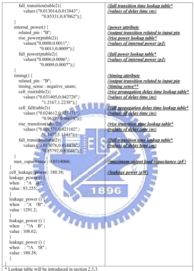
We take a section of our standard cell for instance (see Fig. 2.3). By this example, we can see the above attributes in a practical .lib file.
cell (NAND2X1) { cell_footprint : nand2; area : 3.92; pin(A) { direction : input; capacitance : 0.00118294; } pin(B) { direction : input; capacitance : 0.00109301; } pin(Y) { direction : output; capacitance : 0.0; function : "(!(A B))"; internal_power() { related_pin : "A"; rise_power(ptable2){ values("0.0009,0.0010",\ "0.0007,0.0007");} fall_power(ptable2){ values("0.0005,0.0007",\ "0.0006,0.0006");} } timing() { related_pin : "A"; timing_sense : negative_unate; cell_rise(table2){ values ("0.026925,0.037688",\ "1.2158,1.219");} cell_fall(table2){ values ("0.0226,0.033009",\ "0.95619,0.96855");} rise_transition(table2){ values ("0.0175,0.020095",\ "1.1532,1.1588");} //cell name //footprint attribute //area attribute //input pin group //direction of pin //input capacitance (pF) //input pin group //direction of pin //input capacitance (pF) //output pin group //direction of pin
//output capacitance (pF)
//logic function related to output pin //power attribute
//output transition related to input pin //rise power lookup table*
//values of internal power (pJ) //fall power lookup table* //values of internal power (pJ) //timing attribute
//output transition related to input pin //timing sense**
//rise propagation delay time lookup table* //values of delay time (ns)
//fall propagation delay time lookup table* //values of delay time (ns)
//rise transition time lookup table* //values of delay time (ns)
13 fall_transition(table2){ values ("0.013014,0.013843",\ "0.85331,0.87062");} } internal_power() { related_pin : "B"; rise_power(ptable2){ values("0.0008,0.0011",\ "0.0011,0.0009");} fall_power(ptable2){ values("0.0006,0.0006",\ "0.0009,0.0007");} } timing() { related_pin : "B"; timing_sense : negative_unate; cell_rise(table2){ values ("0.031405,0.042728",\ "1.2167,1.2238");} cell_fall(table2){ values ("0.024612,0.027471",\ "0.96379,0.96674");} rise_transition(table2){ values ("0.020571,0.021102",\ "1.1477,1.1341");} fall_transition(table2){ values ("0.013076,0.014476",\ "0.85792,0.85046");} } max_capacitance : 0.0314066; } cell_leakage_power : 180.38; leakage_power () { when : "A B" ; value : 83.255; } leakage_power () { when : "A !B" ; value : 1291.2; } leakage_power () { when : "!A B" ; value : 108.62; } leakage_power () { when : "!A !B" ; value : 180.38; } }
//fall transition time lookup table* //values of delay time (ns)
//power attribute
//output transition related to input pin //rise power lookup table*
//values of internal power (pJ) //fall power lookup table* //values of internal power (pJ) //timing attribute
//output transition related to input pin //timing sense**
//rise propagation delay time lookup table* //values of delay time (ns)
//fall propagation delay time lookup table* //values of delay time (ns)
//rise transition time lookup table* //values of delay time (ns)
//fall transition time lookup table* //values of delay time (ns)
//maximum output load capacitance (pF) //leakage power (pW)
* Lookup table will be introduced in section 2.3.3.
**A function is said to be unate if a rising (or falling) change on a positive (or negative) unate input variable causes the output function variable to rise (or fall) or not change.
14
2.3.1 Classification of Power [4] [5]
We know that the total power is composed of the dynamic power and the static power. The dynamic power consists of switching power and internal power. We classify these components respectively in the following paragraph.
(1) Switching power: The switching power can be expressed as :
(
)
( )∑
∀ ⋅ = i Nets i Load DD Switching C ToggleRate V P i 2 2 (2.4) The logic transitions at each net will charge/discharge the load capacitance connected to it. At this time, circuits have to consume the power and we call this kind of power consumption as switching power consumption. As shown in Eqn. (2.4), we know that the switching power is related to supply voltage, load capacitance, and toggle rate. First, the operating condition of the cell library with Synopsys model will record the supply voltage. Second, we can derive the load capacitance from the input capacitance of the device model and the load capacitance of the net. Because we can derive the information of the toggle rate of each node by the vectors simulation and statistics implemented, we don’t derive the switching power from the power model of the device but from the calculation by the synthesis tool. By the above description, if we have the information of correct load capacitance and the toggle rate, the synthesis tool can calculate the switching power automatically.So we just have to focus on the power models of the internal power and the leakage power. The switching power will be calculated by the synthesis tool.
(2) Internal power:
The definition of the internal power defined by Synopsys consists of short-circuit power and the power consumed by charging/discharging internal parasitic capacitance
15
of the cell. The internal parasitic capacitances include the interconnection of the MOSs connected by metal lines and the source/drain to substrate equivalent capacitance. The input transition will charge/discharge these internal parasitic capacitances. This kind of power is called internal power consumption. When we calculate the internal power consumption, we have to sum up the power of each pin including the input and output pin. The synthesis tool will sum up a power value from the internal power model of each pin when the pins transit. The unit of the internal power value that the synthesis tool calculates is energy not power as shown in Eqn. (2.5).
(
)
( )∑
∀⋅
=
i CellPins i i talInternalTo
E
ActivityFa
ctor
P
(2.5)where the Ei is the energy of each pin including the input and output pin and the
ActivityFactori is the toggle rate of each pin.
Because we have to sum up the power of each pin including the input and output pin, we need to avoid double calculating the internal power consumption in each pin group when we establish the model. Therefore, the internal power model is just related to the input transition time.
When we calculate the power consumption which is produced by the output pin transition, we can realize that the power of the output pin is related to input transition time and output load capacitance. Even if there is no output transiting, there is still power consumption with the transient of the input pin. We can view it as this power consumption is contributed by the input pin and record this value as the power of the input pin. The two indices of output pin power consumption and the two indices of the pin- to-pin delay are the same with each other, so we can characterize the output pin power and pin-to-pin delay at the same time. We demonstrate the steps to calculate the power of the output pin.
16
First we record the value of power consumption during characterization procedure. Then we have to subtract the power of the input pin and the switching power of the output load capacitance from this value. Thus we can get the power of the output pin and avoid double calculating the power consumption by the subtraction step.
We take a common master-slave DFF without set and reset pin for instance and we set the following situation. The input pin D remains constantly and CLK remains the transient state. So the output pin Q will not change its state. But we know that the transistors in this cell will still turn on and off even if the output pin doesn’t transit due to the conduction path inside the cell. So we realize that there is also power consumption at this time. In this case, we suppose that the output pin does not transit its state if we want to measure the input pin power. We know that the power of the input pin is only related to the input transition time but not related to the output load capacitance.
On the other hand, the transient of the output pin is related to the input pin CLK but not related to the input pin D in this case. So the power consumption of the output pin that we will measure would contain the power consumption produced by the output pin transition and the input CLK transition at the same time. If we only want to get the power of the output pin, we have to dismiss the power produced by the input CLK in order to avoid double calculating. Through these steps, the synthesis tool can calculate the power consumption produced by each pin respectively. By the above description, we know that if a input pin transit its state but the output pin doesn’t, the power consumption is viewed as contributed by input pin and if the input pin and output pin transit their states simultaneously, the synthesis tool will calculate the power consumption by summing up the values from the lookup table of the input and output pins.
17
(3) Leakage power:
The leakage power can be expressed by the following equation:
( )
∑
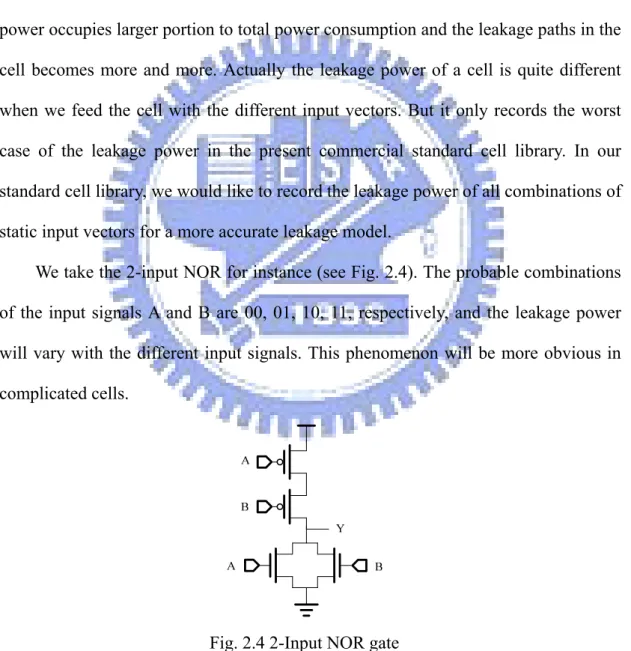
∀ = i Cells e CellLeakag al LeakageTot P P (2.6)The leakage power has three main segments: The reverse junction current of a MOS between drain (or source) to substrate, the sub-threshold current and the DC current. The method that is used to measure the leakage power is assigning the static input vectors to the cell. As the process scales down to deep submicron, the leakage power occupies larger portion to total power consumption and the leakage paths in the cell becomes more and more. Actually the leakage power of a cell is quite different when we feed the cell with the different input vectors. But it only records the worst case of the leakage power in the present commercial standard cell library. In our standard cell library, we would like to record the leakage power of all combinations of static input vectors for a more accurate leakage model.
We take the 2-input NOR for instance (see Fig. 2.4). The probable combinations of the input signals A and B are 00, 01, 10, 11, respectively, and the leakage power will vary with the different input signals. This phenomenon will be more obvious in complicated cells.
Fig. 2.4 2-Input NOR gate
It only records the maximum leakage power in the present commercial standard cell library. But we realize that the leakage power becomes more dominant to total
18
power consumption and how to estimate the leakage power accurately is very important. If there is still only maximum leakage power stored in the novel standard cell library, it will estimate the total power consumption excessively. So we would like to establish our .lib file with the leakage power information that is input dependent.
2.3.2 Classification of Time
Fig. 2.5 Transition time and propagation delay time
There are two main kinds of timing performance. One is the transition time and the other one is the propagation delay time. The definition of the transition time is different in the library supported by different corporations. It may be the time for the signal level changes from 10% to 90%, 20% to 80% or 30% to 70 % of the power supply. But there is only one definition of the propagation delay time. It is defined by the time difference between 50% input signal to 50% output signal as shown in Fig. 2.5.
We take the combinational circuit for instance to explain how to express the propagation delay time. We can realize that the propagation delay time is related to the input transition time and output load capacitance and we express this relation in the Eqn. (2.8). This equation is a linear model where the unit of Kload is ns/pF, and the
19
unit of Cload is pF.
Cell delay = pin to pin intrinsic delay + Kload*Cload (2.6)
There is another non-linear delay model (NLDM) using the input transition time and output load capacitance as two indices to establish the timing table. When we synthesize a circuit, the STA tool can find out the correct delay time from the NLDM table automatically. When the process advances to the deep submicron generation, NLDM is more accurate than the linear delay model. So NLDM is the most popular timing model in the present commercial standard cell libraries. Fig. 2.6 shows NLDM model. Designers can determine the approximate propagation delay by solving the A, B, C, and D coefficients of Eqn. (2.9). Then we insert the coefficient values into Eqn. (2.7) to determine z which is related to the fall propagation delay. We will demonstrate the flow about finding out the wanted fall propagation delay, Z.
Z = A + B.x + C.y + D.x.y (2.7)
Fig. 2.6 Non-Linear Delay Model (NLDM) example
We can derive the coefficients A, B, C, and D first by the Gaussian elimination. Then we use these coefficients A, B, C, and D to find out the wanted fall cell delay, z. For example, we use following equations to find out the coefficients of Eqn. (2.7)
20 first. 0.227 = A + B * 0.098 + C * 0.03 + D * 0.098 * 0.03 0.234 = A + B * 0.098 + C * 0.06 + D * 0.098 * 0.06 0.323 = A + B * 0.587 + C * 0.03 + D * 0.587 * 0.03 0.329 = A + B * 0.587 + C * 0.06 + D * 0.587 * 0.06 Î A =0.2006, B = 0.1983, C = 0.2399, D = 0.0677
Then we want to find out the fall cell delay, z, with input transition time, x, is 0.32 and output capacitance, y, is 0.05. So we take the above coefficients and x=0.32 and y=0.05 into Eqn. (2.7) to solve the fall cell delay, z, is 0.2771.
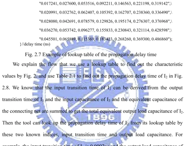
2.3.3 Create Look-up Table
NLDM is used to establish the timing model and power model in .lib file. It uses the lookup table to record timing and power information. The two indices of the lookup table are input transition time and output loading capacitance. We take a section of lookup table for instance (see Fig. 2.7). The title, cell rise, means that it is a look up table to record the propagation delay time of the cell when the output signal transits from low to high. The “tmg_ntin_oload _7x7” means that this look up table uses the tmg_ntin_oload _7x7 to be its template and we can know what the two indices, index_1 and index_2, stand for from that table. The “7x7” means that the table is a 7 by 7 matrix. The “index_1” represents that the input transition time and the unit is ns. The “index_2” represents the output load capacitance and the unit is pF. The values represent the propagation delay time of the cell with the combination of the different input transition time and different output loading capacitance and the unit of these values is ns. The internal power is also recorded in this kind of the lookup table. The values in the internal power table are energy and the unit is pJ.
21 cell_rise(tmg_ntin_oload_7x7) {
index_1("0.011174, 0.051191, 0.091174, 0.142020, 0.263899, 0.434953, 0.660005");//input transition time (ns) index_2("0.000000, 0.001516, 0.006839, 0.017004, 0.032841, \ 0.055062, 0.084301"); //output loading cap. (pF)
values("0.008674, 0.014361, 0.032649, 0.066906, 0.119974, 0.194454, 0.292436",\ "0.013862, 0.022335, 0.044519, 0.079757, 0.132954, 0.207426, 0.305412",\ "0.017241, 0.027600, 0.053516, 0.092211, 0.146563, 0.221198, 0.319142",\ "0.020991, 0.032762, 0.062407, 0.105392, 0.162707, 0.238360, 0.336490",\ "0.028080, 0.042691, 0.078579, 0.129826, 0.195174, 0.276307, 0.376968",\ "0.036270, 0.053742, 0.096277, 0.155833, 0.230843, 0.321114, 0.428598",\ "0.045501, 0.065889, 0.115369, 0.183423, 0.268260, 0.369300, 0.486860"); }//delay time (ns)
Fig. 2.7 Example of lookup table of the propagation delay time
We explain the flow that we use a lookup table to find out the characteristic values by Fig. 2. and use Table 2.1 to find out the propagation delay time of I2 in Fig.
2.8. We know that the input transition time of I2 can be derived from the output
transition time of I1 and the input capacitance of I3 and the equivalent capacitance of
the connecting net are summed to get the total equivalent output load capacitance of I2.
Then the tool can look up the propagation delay time of I2 from its lookup table by
these two known indices, input transition time and output load capacitance. For example, the input transition time of I2 is 0.0092ns and the output load capacitance of
I2 is 0.0015pF, then, the propagation delay of I2 is 0.0269ns.
Fig. 2.8 Example of using lookup table
22
Table 2.1 The lookup table of 2-input NAND
Delay time (ns) Input transition time (ns)
0.0092 0.0491 0.0892 output load
capacitance(pF)
0.0015 0.0269 0.0376 0.0474 0.0067 0.0696 0.0713 0.0818
2.4 Design of Standard Cell Library
We have introduced the overviews of the standard cell library, and the content of the liberty File. Then we will begin to design our standard cell library. We have to decide which kinds of cell shall be included in our standard cell library at the first step. Second we have to define the timing, power and area specification of each cell. We run the simulation and tune the size of each cell to meet the specification at the third step. Then we draw the layout of each cell according to the tuned size. After we draw the layout, we have to use tool to characterize the performances of the cell with layout parasitic. We create the data sheet, synthesis models by the characterized results and the HDL models for the synthesis and automatic placement and route tools at the sixth step. Finally, we have to verify if the standard cell library can function normally in the cell base design flow finally.
We use Fig. 2.9 to explain the flow of characterization. At the first step, we have to prepare the LPE netlist, the SPICE models, the environment setup file, the signal generation file, the header file and the load file. At the second step, we characterize the cells by using the characterization tool, PAREX, which is established by Industrial Technology Research Institute (ITRI). The characterization tool, PAREX, will produce the SPICE simulation file and produce simulation results automatically. Then we put Synopsys templates, verilog templates, and the layout data into PAREX translator and it will translate the results to Synopsys models, verilog models, and the manual for users.
23 Specification Define Circuit Design Layout Design Characterization (PAREX) Data book HDL models Synthesis models Verification (DACCA) S E PAREX Extraction commands PAREX translators Environment Setup File Signal Generation Control files Header Files LPE netlist Load file SPICE models SPICE Simulation Files SPICE Simulator SPICE results Synopsys templates Synopsys models Verilog templates Verilog models Layout Date (Sum Report) Data for Manual Maker Extract characteristic values Data processing
Fig. 2.9 The design flow of creating a standard cell library [5]
2.5 Summary
We have introduced different kinds of power dissipation in the CMOS circuit, the common format of standard cell library and the content of the liberty file. Then we explain the flow that we design and characterize the standard cell. We also introduce the NLDM lookup table of timing and power in the liberty file in this chapter.
24
Chapter 3
Timing and Power Model
Characterization Flow
3.1 Timing Characterization Flow
3.1.1 Transition Time and Propagation Delay time
In this section, we will introduce the flow that we characterize the propagation delay time and transition time. The propagation delay time and transition time actually can be characterized at one simulation. The procedures that we characterize the propagation delay time and transition time are described as following:
(1) The first step: Determining the size of lookup table and choosing the ranges of indices. The way of selecting the ranges of indices can refer to the following rule.
( i ) The minimum index of input transition time:
We use the cell with the largest driving ability to drive the cell with the smallest driving ability in the standard cell library. Then we can obtain the output transition time of the largest driving ability cell. It is defined as the minimum index of input transition time because this is the best timing case that one gate can drive the loading cell. Taking the inverter gate for instance,
25
we use the largest driving ability inverter to drive the smallest driving ability one. Then the output transition time of that largest driving ability inverter is defined as the minimum index of input transition time.
( ii ) The maximum index of input transition time:
We can see that the curves of the input transition time vs. the propagation delay time in Fig. 3.1 are close to be a straight line on the larger segments of the input transition time. As long as the maximum index of transition time is large enough, we can calculate the output propagation delay time that is out of the maximum index by linear extrapolation.
( iii )The maximum index of output loading capacitance:
The rule that we define the maximum index of output loading capacitance is the same with the rule of defining the maximum index of input transition time. The curve of the output loading capacitance vs. the propagation delay time is also close to be a straight line on the larger segments of the output loading capacitance. So we define three times of the largest driving ability inverter input capacitance as the maximum index of output loading capacitance. We also can calculate the output propagation delay time that is out of the maximum index by linear extrapolation.
26 (a) 2.2u 2.1u 2.0u 1.9u 1.8u 1.7u 1.6u 0 100p 200p 300p 400p 500p 600p 700p 800p 900p 0 100p 200p 300p 400p 500p 600p 700p 800p 900p 200p 240p 120p 160p 80p 40p
Input transition time (s)
0 100p 200p 300p 400p 500p 600p 700p 800p 900p 200p 240p 120p 160p 80p 40p High-Vt Mix-Vt (b) (c)
Fig. 3.1 (a) Power vs. input transition time (b) Delay_rise vs. input transition time and (c) Delay_fall vs. input transition time with fixed output load capacitance of an inverter
The size of the lookup table can be determined by the following observations. From Fig. 3.2, we can realize that the curves of the input transition time vs. the propagation delay time or the output loading capacitance vs. the propagation delay time are non-linear on the smaller index and linear on the larger index. So we use the tactic that we choose finer and more indices on the smaller index
27
region and fewer indices on the larger index region to establish the lookup table after determining the minimum and maximum values of index. By this way, we can describe the curve more accurately.
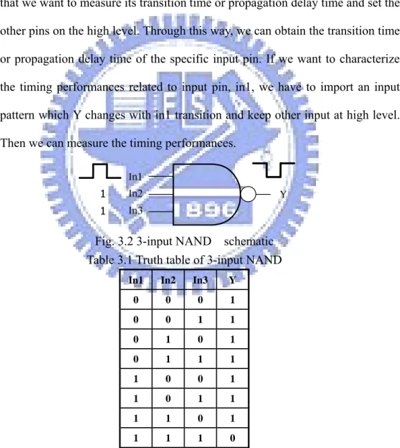
(2) The second step: Determining and importing the input pattern according to the functions of different kinds of cells
− We use a 3-input NAND gate as shown in the Fig. 3. to explain this step. Table 3.1 is the truth table of a 3-input NAND gate. We transit the specific input pin that we want to measure its transition time or propagation delay time and set the other pins on the high level. Through this way, we can obtain the transition time or propagation delay time of the specific input pin. If we want to characterize the timing performances related to input pin, in1, we have to import an input pattern which Y changes with in1 transition and keep other input at high level. Then we can measure the timing performances.
Fig. 3.2 3-input NAND schematic Table 3.1 Truth table of 3-input NAND
In1 In2 In3 Y 0 0 0 1 0 0 1 1 0 1 0 1 0 1 1 1 1 0 0 1 1 0 1 1 1 1 0 1 1 1 1 0
We can find out the combinations of the input pattern that can fit our above requirement are the fourth pattern and the eighth pattern in the Table 3.1.
28
(3) The third step: Run the SPICE simulation and get the results.
Before we run the SPICE simulation, we have to know the following definitions about timing performance.
− Transition time: The definition of transition time is the time difference between 10% VDD and 90% VDD of the output signal. (It also can be from 20% to 80% VDD or from 30% to 70% VDD.)
− Delay time: The definition of delay time is the time difference between 50% VDD of the input signal and 50% VDD of the output signal.
Thus we follow the above three steps and definitions to measure the timing performance.
3.1.2 Input Capacitance
In this section, we will explain the flow that we measure the input capacitances of the cells
(1) Create a lookup table of output load capacitance vs. delay time:
In the first step, we will create a look up table of output load capacitance vs. delay time. We use an arbitrary inverter to drive many different values of capacitance and record the propagation delay time of every simulation. Then we can create the look up table that we want. Fig. 3. and Table 3.2 show what we have to do in this step.
(2) We use the same inverter that we use at the first step to drive the specific input pin of the cell under measurement and then record the delay time of every simulation. Fig. 3.4 shows the action to execute this step.
29
Fig. 3.3 Circuit diagram of creating capacitance vs. delay time look up table Table 3.2 Capacitance vs. Delay table
Capacitance 1fF 2fF 3fF 4fF Delay time 1ps 2ps 3ps 4ps
Fig. 3.4 Use the inverter in step 1 to drive circuit under measurement
(3) In this step, we have to compare the delay time that we have measured in the step 2 with the lookup table created in the step 1. Then, we can find the input capacitance of the cell under measurement from the corresponding delay time in the lookup table. If the delay time of the cell is not exact in the look up table, we can use the interpolation to get the input capacitance.
3.2 Power Characterization Flow
3.2.1 Internal Power
The flow that we characterize the internal power is the same with the transition time andpropagation delay time. So we can characterize them at the same time. There is one thing that we have to notice. The values stored in the internal power table are energy and the unit of these values is joule. It can be expressed by the following equation.
Energy = Power * Time = V(VDD) * I(VDD) * Time
30
the switching power and the energy of the VDD and VSS and at the same time. So it will subtract the switching power from the total power to get the internal power and avoid double calculating the internal power consumption in each pin group. At this time, the tool will also record the energy of VDD and VSS as the output transits, and sum up these two values to obtain the energy consumption in this transition.
3.2.2 Leakage Power
We know that the leakage power of a cell is quite different when we feed the cell with the different input vectors. So we would like to record the leakage power of all combinations of static input vectors. The flow that we characterize the leakage power is described in the following steps.
(1) We import all combinations of static input vectors and measure the power consumption.
(2) We record all power consumptions of the corresponding combinations of input vectors.
Table 3.3 is the leakage power of a 2-input NOR gate and Fig. 3.5 shows an example of input dependent leakage power in the .lib file.
Table 3.3 Leakage power of a 2-input NOR gate
Input AB 00 01 10 11 Leakage power (pW) 353.42 231.18 2795.10 90.46
31 cell_leakage_power : 2795.1; leakage_power () { when : "A B" ; value : 80.462; } leakage_power () { when : "A !B" ; value : 2795.1; } leakage_power () { when : "!A B" ; value : 231.18; } leakage_power () { when : "!A !B" ; value : 353.42; }
//maximum leakage power of cell //input dependent leakage power block //leakage power when input is 11 //leakage power when input is 10 //leakage power when input is 01 //leakage power when input is 00
Fig. 3.5 Example of input dependent leakage power format
3.3 Summary
We have introduced our characterization flow of timing and power model in this chapter. The major difference in our characterization flow is that we create the input dependent leakage power model. It can help the designers to estimate the leakage power more accurately especially in the 90nm or below process. We cooperate with ITRI-STC and use the automatic characterization tool – PAREX established by ITRI-STC to finish our characterization flow.
32
Chapter 4
Low Power Standard Cell Library
4.1 Overview of Low Power Standard Cell Design
Methodology
There are many design methodologies to design low power circuits. It can be assorted as circuit/logic level, technology level, system level, algorithm level, and architecture level. In this thesis, we focus on circuit and logic level to design a low power standard cell library. We know that total power consumption includes both dynamic power and static power from Eqn. (2.1). Therefore, the total power consumption will be reduced as a result of diminishing either dynamic power consumption or static power consumption. The dynamic power consumption can be expressed by the follow equation:
f
V
C
P
dynamic=
α
⋅
L⋅
DD2⋅
(4.1)Where α is toggle rate, CL is output loading capacitance, VDD is supply voltage
and f is operating frequency.
From this equation, we know that we can curtail the switching activity of the nets, output load capacitance, supply voltage, and operating frequency to reduce dynamic power consumption. The main methods that we can do to achieve this target in the
33
standard cell library is shrinking the widths of devices or using low supply voltage cells. Shrinking the widths of devices can also reduce the parasitic capacitance and gate capacitance of the device. It is equivalent to reduce the output load capacitance CL of the cell. The other method, using low supply voltage, would reduce the
performance of cells and the dynamic power consumption at the same time. So, designers can use multiple supply voltages in a chip. The final target is to reduce the total power consumption while meet the required performance. Of course we can also reduce the power consumption by diminishing the leakage power. Eqn. (2.3) provides the information that the leakage power is related to leakage current directly. Thus, we can decrease leakage power by reducing leakage current. We will introduce several techniques to reduce leakage current in the following sections.
4.1.1 Multiple Threshold Voltage Circuit
Multiple-threshold CMOS circuit means that there are at least two different kinds of threshold transistors in a chip. Transistors with different threshold voltages have distinct characterizations. High threshold transistors are used to suppress sub-threshold leakage current, but it will degrade the performance seriously. The utility of low threshold transistors is to achieve high performance, but its sub-threshold leakage current is much greater than the high threshold transistors. The effect of standard threshold transistors is between low and high threshold transistors. According to the above description about multiple threshold technology, there have been several proposed multiple thresholds CMOS design techniques.
The first type is Multi-threshold-Voltage CMOS (MTCOMS) circuit which was proposed by inserting high threshold devices in series to low-Vth circuitry [7]. Fig. 4.1(a) shows the schematic of a MTCMOS circuit.
34
(a) (b) (c)
Fig. 4.1 Schematic of MTCMOS circuits (a) Original MTCMOS (b) PMOS insertion MTCMOS and (c) NMOS insertion MTCMOS
The utility of the sleep control transistor is to do efficient power management. When circuit is in the active mode, the pin SL is applied to low and the sleep control transistors (MP and MN) with high-Vt are turned on. Because the on-resistances of sleep control transistors are very small, the virtual supply voltages (VDDV and VSSV) are quite close to real ones. When the circuit is turned into the standby mode, the pin SL is set to high, MP and MN are turned off and they can cut the leakage current efficiently. Actually, in the practical design, it needs only one type of high-Vt transistor for leakage control. Fig. 4.1(b) and (c) show the PMOS insertion and NMOS insertion schemes, respectively. Most designers prefer the NMOS insertion due to the on-resistance of NMOS is quite smaller than PMOS with the same size. So designers can use the smaller size NMOS to be the sleep control transistor. MTCMOS can be easily implemented based on existing circuits. However, the main drawback of MTCMOS is it can only deal with the standby leakage power. The other problem is the large inserted MOSFETs will increase the area and delay significantly. Besides, if
35
the data retention is required in standby mode, it needs an additional high-Vt memory circuits to maintain the data [8].
The second type of multiple-threshold CMOS circuit is super cut-off CMOS (SCCMOS). The schematic of PMOS and NMOS insertion SCCMOS circuits are shown in Fig. 4.2(a) and (b), respectively. SCCMOS uses rather low-Vth transistors with an inserted gate bias generator than high-Vt sleep control transistors used in MTCMOS [9]. VDD MP VDDV VSS Standby: VDD+0.4V Active: VSS (a) (b) Fig. 4.2 Schematic of SCCMOS circuits (a) PMOS insertion SCCMOS
and (b) NMOS insertion SCCMOS
For the PMOS insertion SCCMOS, the gate is applied to VSS and the low-Vt PMOS is turned on in the active mode. At this time, the virtual supply voltage (VDDV) is very close to real power supply voltage. When the circuit is turned into the standby mode, the gate is set to VDD+0.4V to fully turn off the low-Vt PMOS. Because the reverse bias is applied to the gate of PMOS, SCCMOS can fully cut off
36
the leakage current. On the other hand, the operation of NMOS insertion is the same as PMOS one. The gate of NMOS is set to VDD in the active mode and VSS-0.4V to fully cut off the leakage current in the standby mode, respectively. With the same reason as MTCMOS, it needs only one type of insertion SCCMOS for leakage control in the practical design.
The third type is Dual Threshold CMOS. We know that high threshold transistors are used to suppress sub-threshold leakage current, but it will degrade the performance seriously. For a logic circuit, high threshold transistors can be assigned in non-critical paths to reduce the leakage current, while the low threshold transistors in the critical paths can maintain the performance. By this method, both high performance and low power can be achieved simultaneously and it doesn’t need any additional transistors. Dual Threshold CMOS circuit is shown in Fig. 4.3. This dual threshold technique can diminish the leakage power during both standby and active mode very well. But the main difficulty of using this method is not all the transistors in non-critical paths can be replaced by high threshold voltage transistors due to the complexity of a circuit or the critical path of the circuit may change, thereby increasing the critical delay [1]. So it is hard for the tools to synthesize circuits with the consideration of this method.
Due to the above reason, designers have to use this technique carefully to avoid changing the critical path of the circuit. Note that this algorithm only deals with the circuits at the gate level. Thus, the transistors in a gate will have the same threshold voltage.
37
Fig. 4.3 Dual-threshold CMOS circuit [1]
The next type is mixed-Vth CMOS circuit scheme. [10] introduced two types of mixed-Vth CMOS circuits. Mixed-Vth schemes can have different threshold voltages within a gate. For type I scheme (MVT1), it is not allowed different threshold transistors in p pull-up or n pull-down networks. In the first step, designers have to find out the MOSs on the critical path. If the MOSs on the critical paths are in p pull-up or n pull-down networks, designers need to replace all of the MOSs in p pull-up or n pull-down networks with the same low threshold voltage MOSs to improve the performance. For example, the MOS transistors in the square (see Fig. 4.4(a)) are on the critical path. In the NOR gate, both p pull-up and n pull-down networks have the MOSs on the critical paths. So we change all the PMOSs and NMOSs for low threshold MOSs. In the inverter gate, we can see that only NMOS is on the critical path. So we just replace the NMOS with low threshold MOS and keep the high threshold MOS in the p pull-up network.
In another scheme of mixed-Vth CMOS circuit (MVT2), it allows different threshold transistors anywhere except for the series connected transistors. The transistors on the series connected networks must be the same threshold MOSs. When using the MVT2 technique, designers have to find out the MOSs on the critical paths, first. This step is the same as MVT1. Then designers have to change all the MOSs on
38
the critical paths on the series networks for low threshold transistors. The main difference between MVT1 and MVT2 is that MVT2 will just replace the MOSs on the critical path on the parallel networks with low threshold MOSs and keep other MOSs with high threshold transistors. For example, the NOR gate in Fig. 4.4(b), both the p pull-up series structure and the n pull-down parallel structure networks have MOSs on the critical path , respectively. With the above description, MVT2 replace all the PMOSs in the series structure at the critical path with low threshold MOSs and replace NMOS in the critical to low threshold transistors. MVT2 keeps other NMOSs on the parallel structure networks with high threshold transistors. The situation of inverter gate is the same as MVT1.
(a) (b) Fig. 4.4 MVT schemes of [10] (a) MVT1 scheme and (b) MVT2 scheme
A new Mixed-Vth (MVT) CMOS design technique is proposed to reduce the static power dissipation on gate-level in [12]. The goal of MVT-Gates is to reduce the leakage within a gate without varying the performance. This will be achieved by replacing normal-Vth transistors with high-Vth and low-Vth transistors. Optimization of a gate should not increase the worst case delay.
39
In a logic cell, stacked transistors usually form the critical path, and the MOSs on it must be low-Vth transistors. We can use different threshold transistors in such a stack to reduce leakage and keep the performance. In MLVT-gates scheme (Fig. 4.5(b)), all the transistors on the critical path are low-Vth transistors and the transistors on the non-critical path are still high-Vth transistors. Another scheme is called MVT-gates. The scheme of MVT-gates is the same as MLVT-gates on the non-critical path, but the MVT-gates use different threshold transistors on the critical path at the same time ( Fig. 4.5(a)). Because we use the high-Vt device to block the leakage current and use the low –Vt device to keep the timing performance.
(a) (b) Fig. 4.5 MVT schemes of[12] (a) MVT-NAND2 and (b) MLVT-NAND2
There has been another method proposed called dynamic threshold CMOS (DTMOS) [1]. The threshold voltage can be altered dynamically to suit the operating state of the circuit in this architecture. When circuit is in the standby mode, a high threshold voltage is given to diminish the leakage current. While a low threshold voltage is allowed for higher current drives in the active mode of operation. Designers can establish the DTMOS by tying the gate and body together [11]. Fig. 4.6 shows the schematic of a DTMOS inverter. The supply voltage of DTMOS is limited by the

![Fig. 2.9 The design flow of creating a standard cell library [5] 2.5 Summary](https://thumb-ap.123doks.com/thumbv2/9libinfo/7495514.115808/35.892.144.707.135.852/fig-design-flow-creating-standard-cell-library-summary.webp)

![Fig. 4.3 Dual-threshold CMOS circuit [1]](https://thumb-ap.123doks.com/thumbv2/9libinfo/7495514.115808/49.892.240.634.127.387/fig-dual-threshold-cmos-circuit.webp)
