國 立 交 通 大 學
電子工程學系 電子研究所碩士班
碩 士 論 文
具倒 T 型閘極之多晶矽奈米線通道薄膜電晶體與氮化矽記憶
體元件之製作與特性分析
Fabrication and Characterizations of Poly-Si Nanowire Thin-Film
Transistor and SONOS Memory Featuring Inverse-T Gate
研 究 生:徐行徽
指導教授:林鴻志博士
黃調元博士
具倒 T 型閘極之多晶矽奈米線通道薄膜電晶體與氮化矽記憶
體元件之製作與特性分析
Fabrication and Characterizations of Poly-Si Nanowire Thin-Film
Transistor and SONOS Memory Featuring Inverse-T Gate
研 究 生:徐行徽 Student:Hsing-Hui Hsu
指導教授:林鴻志博士 Advisor:Dr. Horng-Chih Lin
黃調元博士
Dr. Tiao-Yuan Huang
國 立 交 通 大 學
電子工程學系 電子研究所碩士班
碩 士 論 文
A Thesis
Submitted to Department of Electronics Engineering & Institute of Electronics
College of Electrical and Computer Engineering
National Chiao Tung University
In partial Fulfillment of the Requirements
for the Degree of Master
in
Electronics Engineering
June 2008
Hsinchu, Taiwan, Republic of China
具倒 T 型閘極之多晶矽奈米線通道薄膜電晶體與氮化
矽記憶體元件之製作與特性分析
研究生:徐行徽 指導教授: 林鴻志 博士 黃調元 博士 國立交通大學 電子工程學系 電子研究所摘要
在本篇碩士論文中,我們利用簡易的邊襯蝕刻技術製作出一種具有多閘極結 構的多晶矽奈米線薄膜電晶體。藉由小體積的奈米線通道對外在電壓敏感度高的 特性,還有倒 T 型閘極的使用,可以獲得較佳的閘極控制能力,進而增進元件的 性能。除此之外,由於強烈的閘極耦合效應,在分離的上閘極加上適當的偏壓, 便可精確地調控臨限電壓。 基於此獨特的獨立雙閘極奈米線電晶體結構,我們也製作了具有奈米線通道 的 TFT-SONOS 記憶體元件。其中元件的兩個閘極分別作為寫入閘和臨限電壓調控 閘,提供更富彈性的寫入與讀取操作。本篇論文中,我們研究並探討了其基本電 性與寫入/抹除特性,此外,我們也發現在上閘極加入適當的偏壓,可以有效增加 寫入的效率,進而獲得較寬的感測區間。Fabrication and Characterizations of Poly-Si Nanowire
Thin-Film Transistor and SONOS Memory Featuring
Inverse-T Gate
Student: Hsing-Hui Hsu Advisor: Dr. Horng-Chih Lin Dr. Tiao-Yuan Huang
Department of Electronics Engineering & Institute of Electronics National Chiao-Tung University
Abstract
In this thesis, a poly-Si nanowire TFT device with multiple-gated configuration was fabricated by utilizing a simple and low-cost spacer etching technique. With the aid of strong coupling effect between the inverse-T gate and the top gate due to the tiny body of the NW channels, the electrical characteristics are greatly enhanced. In addition, the threshold voltage is capable of being finely tuned with a proper gate bias.
Based on this unique independent double-gate structure, NW TFT-SONOS memory devices were also fabricated and characterized. The two gates which function as programming gate and threshold voltage adjusting gate, respectively, provide flexibility for programming and reading operations. The electrical characteristics including program/erase properties were also studied. Additionally, adding an adequate top-gate bias is found to improve the programming efficiency, resulting in larger memory window.
誌 謝
首先要感謝的是我的指導教授,黃調元博士與林鴻志博士。黃老
師寬廣的眼界與嚴謹的態度使我獲益匪淺,而林老師對研究的熱忱與
對觀念的重視更是鼓舞我積極向前。老師們的所有建議與話語我都將
銘記在心,品味再三。接下來要感謝的是所有曾為實驗室付出過的學
長們:盧文泰博士、葉冠麟博士、李耀仁博士、呂嘉裕博士、李明賢
博士、林宏年博士、蘇俊榮學長、盧景森學長、張伊鋒學長、李聰杰
學長、藍文廷學長、林賢達學長、房新原學長,因為你們的努力,實
驗室才能成長茁壯,生氣蓬勃。再來是同期的碩班夥伴們:趙志誠、
謝雨霖、黃健銘、蔡銑泓、洪振家、呂建松,雖然你們早已畢業,但
是曾經有過的情誼是無法被輕易抹滅的。而唯一伴我四年的張凱翔同
學,一起努力打拼的日子,研究上與生活上的交流,這段時間真的承
蒙照顧,感激不盡。還有畢業的學弟妹們:曾經帶過的黃建富和李克
慧,感謝你們認真的實驗態度,讓我在做研究時事半功倍,無須操心。
現在博一的學弟們:感謝陳威臣在生活上和英文方面的協助,讓我這
懶人不至於與現實脫節,當然還有許多實驗上大大小小的協助;而蔡
子儀也無私地提供了很多製程上的幫助。再來是現在碩二的學弟妹
們:劉大偉、江忠祐、洪政雄、陳玲、李冠樟、林漢仲、洪文強,你
們每個都非常優秀,我也都很喜歡,和你們研究討論的過程使我不斷
地自我成長,也從你們身上獲得不少新知,歡樂但認真的態度讓研究
不再這麼枯燥乏味,感謝你們賜與的美好時光。
結束意味著另一段的開始。但此時此刻,只願此情此景長存我心。
希望大家永遠幸福快樂。
Contents
Abstract………...……..…...i
Acknowledgement...iii
Contents………...iv
List of Figure Caption………...vi
Chapter 1 Introduction 1-1 Overview of Nanowire Technology………...1
1-2 Multiple-gated Transistors………...2
1-3 Overview of Nonvolatile Memory………...3
1-3.1 SONOS Flash Memory………...4
1-3.2 Nanowire Nonvolatile Memory………...5
1-4 Motivation………6
1-5 Thesis Organization………...6
Chapter 2 Poly-Si Nanowire Thin-Film Transistors with Inverse-T Gate 2-1 Device Fabrication and Measurement………...…………8
2-1.1 Device Structure and Process Flow………..8
2-1.2 Electrical Characterization and Measurement Setup………...……9
2-2 Fundamental Electrical Characteristics……....………...…...10
2-2.1 Gate Fringing-field Effect………...………...11
2-2.2 ITDG-NWTFT with Thinner NW Body.………...12
2-3 Device Characteristics with Independent Double-gated Operation……...12
Chapter 3 Nanowire TFT-SONOS Memory with Inverse-T Double Gate 3-1 Device Fabrication and Operation Principles………16
3-1-1 Device Structure and Process Flow………...………....16
3-1-2 Program/Erase Operation Principles………...16
3-2 Program/Erase Characteristics………...17
3-3 Reliability Characteristics……..………...18
3-3-1 Retention...………...…….18
3-3-2 Endurance……….…….………19
Chapter 4 Conclusions and Future Works 4-1 Conclusions………...21 4-2 Future Works...22 References………...23 Figures………...28 Vita……..………...51
List of Figure Caption
Chapter 2
Fig. 2-1 Top view and cross-sectional view of inverse-T gate NWTFT (a) and inverse-T double-gate NWTFT (b)………...28 Fig. 2-2 (a) Deposition of in-situ-doped n+ poly-Si. (b) Definition and formation of
inverse-T gate. (c) Deposition of inverse-T gate oxide and poly-Si active layer. (d) Source/Drain ion implantation. (e) Definition of source/drain and formation of NW channel (ITG structure). (f) Deposition of top gate oxide and formation of top gate (ITDG structure)..………..29 Fig. 2-3 Cross-sectional TEM image of NW channels with inverse-T gate……….…32 Fig. 2-4 Transfer characteristic of ITG-NWTFT and compared with single side-gate structure………...33 Fig. 2-5 Transfer characteristics of ITDG-NWTFT operated in single-gated (SG)
modes and double-gated (DG) mode………...34 Fig. 2-6 (a) Transfer and (b) output characteristics of ITG NWTFT versus ITDG
NWTFT………...35 Fig. 2-7 Current ratio of ITDG-NWTFT to ITG-NWTFT at different VG – VTH
value……….36 Fig. 2-8 Schematic illustration of fringing-field effect caused by inverse-T gate…….36 Fig. 2-9 Cross-sectional TEM images of the ITDG structure and NW channel
profile………...37 Fig. 2-10 Transfer characteristics of ITDG-NWTFT operated in SG modes and DG
mode with thinner NW channel………...38 Fig. 2-11 Transfer characteristics of ITDG devices by sweeping inverse-T gate voltage
as top gate biased at various constant values………...39 Fig. 2-12 Extracted VTH and SS from Fig. 2-11 (a) as functions of top gate voltage.
(Thicker NW channel)……….40 Fig. 2-13 Extracted VTH and SS from Fig. 2-11 (b) as functions of top gate voltage. (Thinner NW channel)……….41 Fig. 2-14 [Ref. 2-2] Schematic potential distributions across the channel and simple
model for independent double-gated structure with ultra thin body………42
Chapter 3
Fig. 3-1 Cross-sectional view of the inverse-T gate poly-Si NW SONOS structure…43 Fig. 3-2 [Ref. 3-1] Energy band diagram of SONOS structure in (a) flat-band condition and (b) FN tunneling under high electric field………44 Fig. 3-3 Transfer characteristics by sweeping inverse-T gate voltage with a fixed bias ranging from 1V to -2V applied to the top gate………45 Fig. 3-4 Transfer I-V curves of programming and erasing states in two different bias conditions……….46 Fig. 3-5 (a) Programming and (b) erasing characteristics of ITDG NW-SONOS device with different top gate biases………...47 Fig. 3-6 [Ref. 3-2] Band diagram of charge loss path in SONOS: thermal excitation
(TE), Frenkel-Poole emission (FP), trap-to-band tunneling (TB), trap-to-trap tunneling (T-T), and band-to-trap tunneling………48 Fig. 3-7 Retention characteristics with (a) ID-VG curves and (b) VTH variation……...49 Fig. 3-8 (a) Transfer characteristics and (b) VTH variation with increasing
Chapter 1
Introduction
1-1 Overview of Nanowire Technology
When a stripe-structured material with a diameter or feature size smaller than 100 nm, it is called nanowire (NW). For a stripe structure, the ratio of the surface area to volume increases as its cross-sectional dimensions shrink. Since NW has very small volume and large surface-to-volume ratio, material properties and carrier transport in NW would be significantly affected by the surface condition. Owning to this inherent property, NWs are attractive for a variety of applications, including nano CMOS [1-1], NW TFTs [1-2], memory devices [1-3], and biosensors [1-4]. For electronic device applications, NW channels exhibit enhanced gate controllability and suppressed short-channel effects. For memory applications, NWs possess high programming efficiency and low voltage operation [1-5]. For sensor applications, its high surface-to-volume ratio provides high sensitivity.
Typically, the preparation methods of NWs can be classified into two groups, one is “top-down” and the other is “bottom-up”. Top-down methods usually involve advanced lithography tools, like deep-UV, e-beam and nano-imprint [1-6], to generate NW patterns. With its capability of precise positioning and good reproducibility, this technique is suitable for mass production. Currently nano-scale lines down to or even
narrower than 45 nm are routinely generated in production lines to fabricate advanced circuitries. Nevertheless, the mature processing techniques still face certain issues. For example, the fabrication cost is extremely high as costly exposure apparatus or expensive materials like silicon-on-insulator (SOI) are used. Moreover, the process usually adopts cutting-edge technology. Therefore, it is hard to be employed widely in universities for research purpose. Finally, the selection of NW material is quite inflexible because of the limitation set by the substrate material.
The bottom-up approaches include metal-catalyzed [1-7], solid-liquid-solid [1-8], oxide-assisted growth [1-9], and so on. The most popular one is metal-catalyzed vapor-liquid-solid (VLS) mechanism. It can be used to synthesize different kinds of materials of NWs. Although bottom-up approaches are significantly cheaper than top-down methods and more flexible for experimental purpose, they have their own shortcomings. First, length, diameter and orientation of NWs are not easy to precisely control. The prepared NWs are difficult to align and position accurately, especially for the purpose of device fabrication. For metal-catalyzed growth, metal contamination is a potential concern. Formation of reliable contacts represents another major issue.
1-2 Multiple-gated Transistors
In the challenges of device shrinking to nano-scale, one critical problem is how to increase the gate controllability in order to suppress short channel effects (SCEs). Reduction of gate oxide thickness can help, but dramatic increase in tunneling current from gate electrode would aggravate power consumption of circuits. Two methods for increasing the gate controllability are feasible, one is to use high-κ materials as gate insulator, and the other is the adoption of multiple-gated structure.
A number of multiple-gated (MG) SOI device structures have been proposed so far [1-10]. In comparison with single-gated device, MG SOI structure can effectively prevent the electric field originating from drain from being penetrated into the channel, thus relieving the SCEs. Among the MG structures, the quasi planar FinFETs have drawn most attention in recent years. The FinFET structure can not only provide MG control over the channel, but also has good ability to shrink the channel dimension into nano-meter scale. Moreover, compared with other MG structures, the principal advantage of FinFET is its quasi-planar structure so that modern fabrication skills could be used. Several types of FinFET structures have been proposed and evolved, including double-gate (DG) (UC Berkeley) [1-11], tri-gate (Intel) [1-12], and Ω-gate (TSMC) [1-13]. The most ideal MG structure is gate-all-around (GAA) MOSFET [1-14], which exhibits best gate controllability over the channel potential.
1-3 Overview of Nonvolatile Memory
In recent years, nonvolatile memory (NVM) plays a more and more important role in the development and research of semiconductor memories. NVM device retains the stored data even if the power is switched off. So it is more convenient for data access and ideally suitable for portable electronic products. One of the most important inventions is FLASH memory, which possesses a number of advantages such as byte-selectable write operation combined with sector “flash” erase, non-volatility, good durability and low power. Therefore it becomes the ideal choice of data storage for numerous electronic systems.
Floating-gate device is the mainstream of flash memory technology to this date. However, as the transistor become smaller, the floating-gate device is confronted with
several scaling limits. Since the storage layer is made of poly-silicon, the narrow spacing between two adjacent memory cells would lead to coupling interference between them, resulting in undesirable threshold voltage shift. Another issue is associated with the scaling of tunnel oxide thickness for reducing the programming/erasing operation voltages. For a thin dielectric, a single defect contained in the thin tunnel oxide would cause all stored charges contained in the conductive floating gate to be lost, thus degrading the reliability of memory device. This limits the thickness of tunneling oxide at around 7 nm. Consequently, it is difficult to further reduce the size of floating-gate device. In the 2005 international electronic device meeting (IEDM), it was pointed out that the next generation flash memory should turn into charge-trapping flash (CTF).
1-3.1 SONOS Flash Memory
Silicon-oxide-nitride-oxide-Silicon (SONOS) multi-layer structure has been widely used in recent charge-trapping flash to overcome difficulties presenting in floating-gate flash [1-15]. SONOS devices replace the poly-silicon storage layer in floating-gate devices with a nitride trapping layer. Since nitride is an insulator, the charges are discretely stored in the trap of nitride. Unlike the case of using floating poly-Si as the storage site, a single defect formed in the tunneling oxide would not cause all charges to leak out through the defect, hence improved data retention characteristic can be obtained. Besides, the SONOS structure has a much reduced height as compared with the floating-gate structure, so the SONOS memory exhibits much stronger immunity against coupling interference. This is extremely important in the progress of memory device scaling. Currently, many studies have investigated the feasibility of applying SONOS structure to thin-film-transistor for the purpose of
system-on-chip (SOC) or system-on-panel (SOP) integration [1-16].The TFT-SONOS array could be stacked vertically to make 3-D configuration, allowing increased device density without aggressively reducing device dimensions.
1-3.2 Nanowire Nonvolatile Memory
Silicon NW (SiNW) has a great potential to shrink memory cells to nano-meter scale without suffering short channel effects (SCEs). Furthermore, due to the inherent large surface-to-volume ratio, electric potential in NW channel is very sensitive to the surface condition. By utilizing this characteristic to nonvolatile memory, a small amount of charge storage could change the threshold voltage of memory device to obtain sufficient memory window, hence program/erase time or voltage could be dramatically reduced.
At present, the proposed concepts and techniques for NW NVM include SONOS [1-17], FRAM [1-18], nano-dot [1-19], molecule-gate [1-20], etc. The principles of above-mentioned techniques are to form a charge-storage layer on the surface of NW, and the charges stored may adjust NW’s conductance to determine the logic state of the device. SONOS and FRAM can build on the development experience of planar devices, and they could be feasible for NW NVM applications in the near future.
1-4 Motivation
To address the issues met in typical top-down and bottom-up approaches for NW device fabrication, our laboratory (ADT Lab) has recently proposed and developed a new poly-Si NW field-effect transistor scheme which cleverly employed the sidewall spacer etching technique to define poly-Si NWs that serve as the device channels. The scheme offers the following advantages:
(1) The fabrication is simple and low in cost. (2) NW channel size can be well-controlled. (3) The NWs can be positioned accurately.
(4) It is easily integrated with modern CMOS manufacturing.
NW channel is shown to be beneficial for enhancing the device performance in our previous works. Nevertheless, only one surface of the triangular NW channel can be manipulated by a single side-gate, thus the insufficient gate controllability would limit device performance. This drawback could be addressed with the use of multiple-gate (MG) structure which tends to increase gate controllability. In addition, each gate can be independently biased in the MG configuration. Such design allows more freedoms for device operation, and may increase its feasibility in NVM device applications.
1-5 Thesis Organization
In this thesis, several types of poly-Si nanowire thin-film-transistor (NWTFT) with multiple-gated (MG) configuration, including inverse-T-gate (ITG), inverse-T double-gate (ITDG) and tri-gate (TG), were fabricated and characterized. In addition, we also proposed and demonstrated a novel independent double-gated NW-SONOS
nonvolatile memory (NVM) by utilizing the ITDG-NWTFT structure.
In Chapter 2, we briefly describe the device structures and process flows of ITG-NWTFT and ITDG-NWTFT, and then present and discuss their electrical characteristics. In Chapter 3, the preliminary results of program/erase characteristics and reliability of ITDG NW-SONOS memory are presented and analyzed. Finally, we summarize the conclusions and our major achievements, and also the suggested future works in Chapter 4.
Chapter 2
Poly-Si Nanowire Thin-Film
Transistors with Inverse-T Gate
2-1 Device Fabrication and Measurement
2-1.1 Device Structure and Process Flow
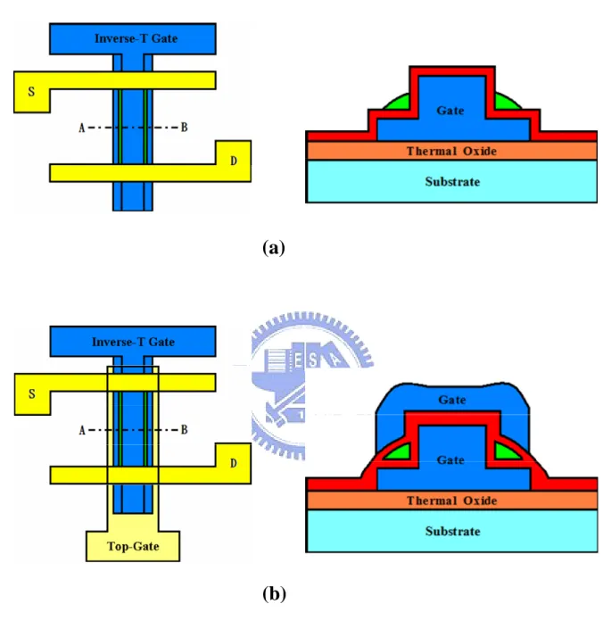
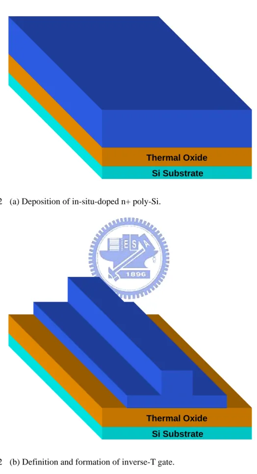
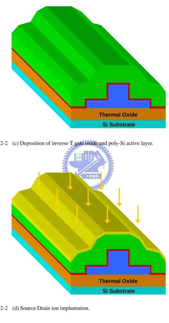
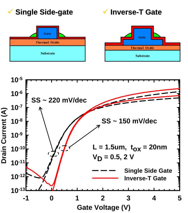
Top views and cross-sectional views of inverse-T gate NWTFT and inverse-T double-gate NWTFT are shown in Fig. 2-1. Schematic flow-charts of the fabrication process for the proposed devices are shown in Figs. 2-2 (a) to (f). Briefly, the fabrication started on 6-inch silicon wafers capped with a 100nm silicon dioxide layer. After depositing a 150nm-thick in-situ-doped n+ poly-Si, the inverse-T gate was formed by twice applying the standard G-line lithography and dry etching steps (Figs. 2-2 (a), (b)). This was followed by the deposition of a 20nm-thick low-pressure chemical vapor deposition (LPCVD) oxide layer serving as the dielectric of inverse-T-gate. A 100nm-thick amorphous-Si layer was then deposited by LPCVD system. Next, an annealing step was performed at 600°C in N2 ambient for 24-hour to transform the amorphous-Si into poly-Si (Fig. 2-2 (c)). Subsequently, source/drain (S/D) implant was performed by P+ implantation at 15keV and 1E15cm-2 (Fig. 2-2 (d)). It should be noted that the implant energy was kept low so that the implanted dopants were distributed near the top surface of the poly-Si layer. After S/D photo-resist patterns were formed, a
reactive plasma etching step was employed to form the nanowire channels simultaneously with S/D definition (Fig. 2-2 (e)). Note that the height of upper step of the inverse-T gate was designed to be higher (100nm) than the lower one (50nm), so the etching time could be controlled to allow only two NW channels remaining on the upper-step corners of the inverse-T gate, and the channel size can be determined by tuning the over-etching time. Wafers were then split into two groups, with either top gate (denote as ITDG) or without top gate (denote as ITG) above the NW channels. Another LPCVD TEOS oxide layer with thickness of 20nm was then deposited to serve as top gate oxide. Then a 100nm-thick in-situ doped n+ poly-Si was deposited and patterned to serve as the top gate electrode (Fig. 2-2 (f)). All devices were then covered with 200nm-thick oxide passivation layer. The fabrication was completed after the formation of test pads using standard metallization steps. All fabricated devices received a NH3 plasma treatment at 300°C for 3-hour before characterization.
2-1.2 Electrical Characterization and Measurement Setup
Electrical characteristics of fabricated devices in this thesis are mainly characterized by an automated measurement setup constructed by HP4156 semiconductor parameter analyzer and Interactive Characterization Software (ICS) program. In all measurements, the temperature was controlled at a stable value by temperature regulated hot-chuck.
From the ID-VG curve at VD = 0.5V, performance parameters of the NW devices including subthreshold swing (SS), threshold voltage (VTH) and field-effect mobility (µFE) can be extracted according to their definition. Subthreshold swing (SS) can be calculated from the subthreshold current in the weak inversion region by
) (logI V SS D G ∂ ∂ = (2-1)
The threshold voltage (VTH) here, calculated by constant current method, is defined as the gate voltage (VG) to achieve a drain current (ID) of (W/L) × 10nA, i.e.,
10nA L W I @ V VTH = G D = × (2-2)
where W and L are the channel width and length, respectively.
Finally, the field-effect mobility (µFE) is determined by
D OX m FE V WC Lg µ = (2-3)
where gm is the maximum trans-conductance and COX is the gate capacitance per unit area.
2-2 Fundamental Electrical Characteristics
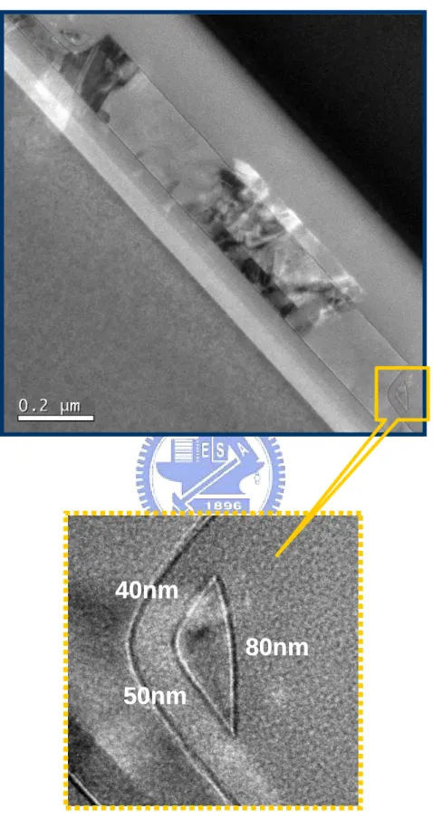
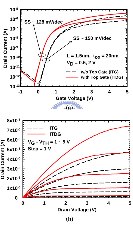
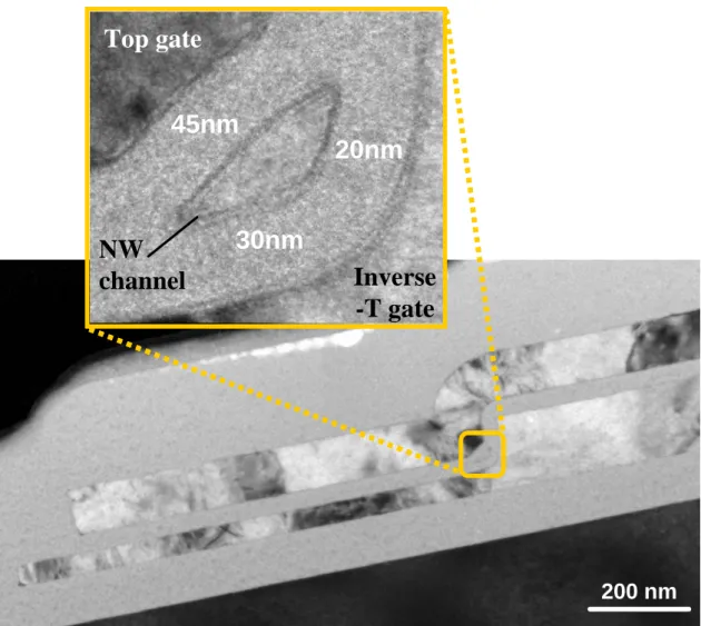
The cross-sectional transmission electron microscopic (TEM) image of NW channels with inverse-T gate is shown in Fig. 2-3. Two NW channels are precisely positioned on the upper-step corners of the inverse-T Gate, and the edge lengths of the triangular NW channel cross-section are 40nm, 50nm, and 80nm, respectively. The transfer characteristics of ITG-NWTFT are shown in Fig. 2-4, together with that of the single-side gated structure for comparison. Owing to NW channels, drain-induced-barrier-lowering (DIBL) in both devices is essentially eliminated. The subthreshold swing (SS) of single side-gate device is 220mV/dec, and for ITG device it is 150mV/dec. So it is apparent that the ITG NW device shows much better performance, such as higher ION and steeper SS. We believe that these phenomena are
due to better gate-controllability of ITG device. Two sides of NW channel can be directly manipulated by inverse-T gate, while single side-gate can only manipulate one side.
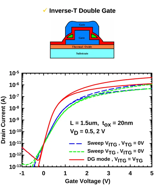
NWTFT with ITDG configuration can be operated in several different modes. Fig. 2-5 shows and compares the transfer characteristics of ITDG-NWTFT operated in two single-gated (SG) modes and double-gated (DG) mode. In SG modes, varying bias is applied to one of inverse-T gate and top gate electrodes with the other one grounded, whereas in DG mode, both the inverse-T gate and top gate electrodes are connected together to serve as a driving gate. Because of larger conducting area and better gate controllability over the NW channels, ITDG device operated in DG mode apparently exhibits higher ON current and steeper subthreshold swing (SS) as low as 128mV/dec. (@VD = 0.5V) is obtained. The transfer and output characteristics of ITG versus ITDG NWTFTs are depicted in Figs. 2-6 (a) and (b) respectively, and reveal that the ITDG-NWTFT (in DG mode) exhibits better device performance.
2-2.1 Gate Fringing-field Effect
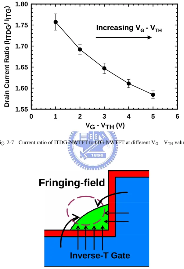
Although the ON current of ITDG NWTFT is reasonably larger than that of ITG one, we observe that, with a increase in gate voltage, the drain current ratio of ITDG to ITG device becomes lower, as shown in Fig. 2-7. Note that the current ratio was measured at drain voltage ranging from 0.1V to VG - VTH for each VG - VTH, and the bars in the figure indicate the deviation of measured data. The trend shown in the figure is postulated to be caused by the gate fringing-field effect. Such effect is schematically shown in Fig. 2-8 and is employed to explain this phenomenon. As VG increases, the NW channel surface conductive area of the ITG device is enlarged by the gate fringing field around the corner regions of the NW channel, therefore the ID would be larger than
expectation. For ITDG device, since the NW channels are surrounded by inverse-T gate and top gate, so no such bonus exists with increasing VG.
2-2.2 ITDG-NWTFT with Thinner NW Body
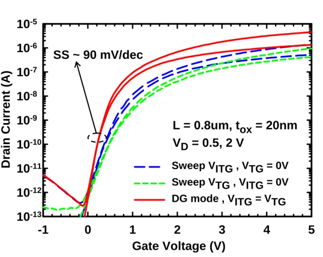
Since the poly-Si NW channel size can be controlled by tuning the over-etching time in the fabrication process, we have also fabricated an ITDG-NWTFT which has thinner and smaller NW body in comparison with previous ITG and ITDG devices by increasing the over-etching time. The cross-sectional TEM images of the device structure and NW channel profile are shown in Fig. 2-9. Both inverse-T gate and top gate oxide are 20nm-thick, and the dimensions of the NW cross-section are down to 20nm, 30nm and 45nm. Fig. 2-10 shows the transfer characteristics operated in SG modes and DG mode. The enhancement of gate controllability over the NW channel under the DG mode resulting in steeper subthreshold swings of 90mV/dec is ascribed to its thinner body. Note that such SS performance is comparable to that of modern CMOS devices, despite the use of polycrystalline channels for the device characterized in this study.
2-3 Device Characteristics with Independent
Double-gated Operation
Due to the small volume and thin body of poly-Si NW, the channel potential is sensitive to both gates, and thus strong gate-to-gate coupling phenomenon can be significant and would allow threshold voltage when operating one of the two gates to be tunable by bias applied to the other gate. An example is shown in Fig. 2-11, in which the
transfer characteristics of ITDG devices by sweeping inverse-T gate voltage are shown as a function of top gate voltage. The NW body of NWTFT is thicker in Fig. 2-11 (a) (see Fig. 3), and thinner in Fig. 2-11 (b) (see Fig. 9). It is apparent to that the threshold voltage can be effectively modulated by the top gate bias. Moreover, Fig. 2-11 (b) also depicts that the VTH of ITDG device can be adjusted more linearly with thinner NW channel. This property could be applied for low standby power circuits. For example, in standby circuit operation, a lower subthreshold leakage can be obtained by raising the VTH of the devices. By adjusting a moderate VTH for active mode, a sufficient driving current can also be provided. Nevertheless, the driving gate (or the inverse-T gate in the present case) has to overcome the impact of the other gate (top gate) on NW channel potential according to the back-gate-effect [2-1]. As a consequence, the subthreshold swing of ITDG device driven only by inverse-T gate with fixed top gate bias (solid lines in Fig. 2-11), is reasonably larger than that of device operated in DG mode (dashed line in Fig. 2-11).
The extracted VTH and SS from Figs. 2-11 (a) and (b) as a function of top gate voltage are depicted in Fig. 2-12 and Fig. 2-13, respectively. The plots are divided into two regions by VTHDG, which is the VTH measured in DG mode of each device. From Fig. 2-12, it can be seen that the VTH shift rate at high VTG (-1V/V) is two times that at low VTG (-0.5V/V). For the device with thinner NW body, Fig. 2-13 shows that the VTH is almost linearly modulated by VTG. The average VTH shift rate is -0.7V/V when VTG is lower than VTHDG and turns into -0.8V/V when VTG is higher than VTHDG. On the other hand, the SS is smaller when VTG is smaller than VTHDG, while larger when VTG is larger than VTHDG in both Fig. 2-12 and Fig. 2-13. It could be explained that, when VTG is smaller than VTHDG, the channel surface near the top gate side is depleted and an inversion layer would form on the inverse-T gate side surface. In this situation the VTH
modulation ability is relatively weak owing to the longer distance between top gate and the inversion layer (the total distance is probably the thickness of top-gate oxide plus the fully-depleted NW body). But when VTG is larger than VTHDG, the inversion layer would form on channel surface along the top gate side first, and the shorter distance between the top gate and inversion layer results in stronger VTH modulation ability, and furthermore the longer distance between inverse-T gate and inversion layer causes the weaker driving-gate controllability leading to higher SS.
To further realize this phenomenon, the simple model with schematic potential distributions described in Fig. 2-14 could be used [2-2]. The G2 is defined as the VTH adjusting gate and G1 as the driving gate. The silicon channel is assumed to be fully depleted, and both the effective TOX1 and TOX2 are multiplied by 3 according to εSi/εSiO2 = 11.9/3.9. Consequently, both Si and SiO2 can be treated as identical dielectrics and the potential distributions can be illustrated as straight lines. According to this simple distribution lines, the VTH(G1) shift rate by VG2 can be easily obtained by using the similarity of ∆ABC and ∆DEC in Fig. 2-14. As a result, the back-gate-effect factor γ = dVTH(G1)/dVG2, which can represent VTH shift rate, becomes smaller as VG2 < VTHDG (γ = 3TOX(G1)/(3TOX(G2) + TSi)) and larger as VG2 > VTHDG (γ = (3TOX(G1) + TSi)/3TOX(G2)). Since the SS is proportional to (1 + γ) analytically, the SS is smaller when VG2 < VTHDG, but lager when VG2 > VTHDG. This model is qualitatively suitable for any device structure with ultra thin body and independent double-gate, and our findings in ITDG device characteristics are essentially consistent with the model.
Chapter 3
Nanowire TFT-SONOS Memory
with Inverse-T Double Gate
Memories featuring thin-film-transistor with SONOS structure (TFT-SONOS) are feasible for flat panel display to achieve system-on-panel (SOP) integration and could be stacked vertically to form 3D configuration for multiplying device density. However, some challenging issues such as poor subthreshold swing and large leakage current existing in conventional TFTs raise the power dissipation concern. By utilizing nanowire (NW) channel in TFT structure, the subthreshold swing and the leakage current can be reduced owing to better gate controllability and much reduced cross-sectional area of leakage path. Furthermore, since the NW channel is sensitive to its surface condition, a small amount of charge storage could shift the threshold voltage and therefore sufficient memory window, leading to shorter program/erase time. In this chapter, we utilize the inverse-T double-gated structure (presented and discussed in Chapter 2) to fabricate TFT-SONOS device configured with poly-Si NW channel and independent double-gate. The electrical characteristics including program/erase properties are studied. Additionally, adding an adequate top-gate bias is found to improve the programming efficiency, resulting in larger memory window.
3-1 Device Fabrication and Operation Principles
3-1.1 Device Structure and Process Flow
Schematic structure of the proposed inverse-T gate NW SONOS device is shown in Fig. 3-1. In this configuration, the inverse-T gate dielectric is replaced by an ONO stacked layer serving as the storage site. Modulation of charge storage in the ONO layer is expected to change the threshold voltage of memory device, and the top gate can be used as an assistant gate for programming and reading by exploiting the gate-to-gate-coupling effect. The fabrication process sequence is similar to that described in Chapter 2. The inverse-T gate dielectric is an ONO multilayer stack consisting of 10nm blocking oxide, 6nm silicon nitride, and 5nm tunneling oxide, all deposited by LPCVD. The top gate dielectric is 20nm-thick LPCVD TEOS oxide. The dry etching condition and parameters of the NW channel are identical to those described in Chapter 2, hence the NW channel profile is similar to the cross-sectional TEM image shown in Fig. 2-3.
3-1.2 Program/Erase Operation Principles
The program/erase mechanisms in SONOS device operation generally include channel hot electron injection (CHEI), Fowler-Nordhiem tunneling (FN tunneling), and band-to-band tunneling (BTBT). Since the existence of potential barrier caused by grain boundaries in poly-Si NW channel would hinder the acceleration of the electrons from source to drain, the CHEI method is not appropriate for programming operation of poly-Si NW-SONOS device. In this chapter, the NW-SONOS device is programmed and erased by FN tunneling mechanism. For programming operation, both source and
drain are grounded, and a highly positive voltage is applied to the control gate to induce strong electric field, and a number of electrons in the channel may tunnel through the thin oxide layer and be trapped by the trapping centers in the nitride layer. For erasing operation, both source and drain are also grounded, and a highly negative voltage is applied to the control gate to detrap electrons in the nitride layer. Fig. 3-2 illustrates the energy band diagram of SONOS structure in flat-band condition (Fig. 3-2 (a)) and FN tunneling under high electric field (Fig. 3-2 (b)) [3-1].
3-2 Program/Erase Characteristics
Owing to the small volume of NW, the channel potential is sensitive to both inverse-T gate and top gate. Therefore the independently applied top gate bias can be used to tune the VTH of NW channels. Fig. 3-3 shows transfer characteristics by sweeping inverse-T gate voltage with a fixed bias ranging from 1V to -2V applied to the top gate. It can be seen that the transfer characteristics are clearly shifted by varying the top gate voltage. Fig. 3-4 shows the transfer I-V curves of programming and erasing states. Two programming and erasing conditions are used (P1: VITG/VTG = 15V/0V, tP = 1ms; P2: VITG/VTG = 15V/5V, tP = 1ms; E1: VITG/VTG = -13V/0V, tE = 10ms; E2: VITG/VTG = -13V/5V, tE = 10ms), and memory windows of more than 2V are achieved. Detailed programming and erasing characteristics as a function of time are depicted in Figs. 3-5 (a) and (b), respectively. It can be seen that both Program and Erase operations exhibit no saturation phenomenon with tP and tE up to 10ms and 1sec, respectively. Fig. 3-5 (a) also shows that programming speed is enhanced by applying 5V to the top gate. This is because by applying a positive top-gate voltage during programming, more electrons could be generated in NW channel, resulting in higher programming efficiency.
However, the erasing characteristics are basically independent of the top gate bias, as shown in Fig. 3-5 (b).
3-3 Reliability Characteristics
For practical application, the nonvolatile memories need to meet some reliability requirements. Data retention capability and program/erase cycling endurance are two main characteristics to evaluate the practicability and reliability of memory cells in practical use.
3-3.1 Retention
The retention of a nonvolatile memory cell refers to the ability of the memory cell to keep the trapped charges from loss for a long duration to retain the stored information. The charge escaping path from trapping-layer could be thermionic emission with Frenkel-Poole mechanism, or tunneling mechanisms through either blocking oxide or tunneling oxide. Fig. 3-6 illustrates the band diagram with charge loss paths in SONOS device [3-2]. The combination of Frenkel-Poole emission (FP) and field-enhanced thermal excitation (TE) can excite the trapped charges, causing them to flow into Si conduction band. For tunneling mechanisms, the trapped electrons in the nitride could tunnel back to the conduction band of Si substrate (trap-to-band tunneling (TB)), or to the interface traps of Si channel (trap-to-trap tunneling (TT)). Besides, holes from Si valence band may tunnel into the nitride traps under the influence of the internal electric field (band-to-trap tunneling (BT)).
electrodes are grounded during the duration of retention measurement. It can be seen that memory window of about 1V can be retained after 10 years. For this NW-SONOS device, thicker tunneling oxide (50Å) is adopted to avoid charge loss by direct tunneling. Nevertheless, the tunneling oxide was fabricated by LPCVD TEOS, and a larger number of defects may form in the TEOS oxide and the interface, compared with the oxide fabricated by thermal dry oxidation. Consequently, field-enhanced trap-assisted tunneling and Frenkel-Poole emission through oxide-trap are considered to be the two major charge loss mechanisms in this NW-SONOS device.
3-3.2 Endurance
Endurance characteristics refer to the reliability of a memory device in terms of the number of program/erase (P/E) operations that can be performed on it without failure. Since high voltage is applied during each program/erase operation, the energetic carriers would degrade the tunneling oxide, more and more oxide-trap and interface-trap states would be generated, resulting in the degeneration of the device performance. Today, most commercially available nonvolatile memory products are guaranteed to endure at least 104 P/E cycles.
The endurance characteristics with ID-VG curves and VTH variation are shown in Figs. 3-8 (a) and (b), respectively. The bias condition for programming is VITG/VTG = 15V/5V, tP = 1ms, and for erasing is VITG/VTG = -13V/0V, tE = 10ms. As cycle number increases, the threshold voltage for both the program-state and erase-state move upward and the memory window narrows. The subthreshold swing worsening is ascribed to the degradation of tunneling oxide, and the memory window closure is attributed to the degradation of the nitride layer. The device is near the state of failure only after 100 program/erase cycles. The poor endurance characteristics may be due to the weaker
bonding strength of TEOS tunneling oxide. Moreover, the tips of the triangular NW channel would induce higher electric field to accelerate the degradation of tunneling oxide.
3-4 Brief Summary
Preliminary results of NW TFT-SONOS we obtained so far are satisfactory. Although the program/erase speed is acceptable, the poor endurance characteristics would hinder its practical application. In addition to the non-optimized structural parameters, such as ONO thickness and NW channel size, the irregular profile of NW and poor quality of TEOS tunneling oxide are postulated to be the main reasons responsible for the outcome.
Chapter 4
Conclusions and Future Works
4-1 Conclusions
In this thesis, a novel multiple-gated (MG) poly-Si NW-TFT featuring inverse-T gate was fabricated and characterized. In the proposed structure, poly-Si NW channels are formed with sidewall spacer etching technique. By further adding a top gate to wrap the NW channels together with the inverse-T gate, enhanced gate controllability over NW channel is achieved, resulting in a higher ON-current, reduced short channel effects and steeper sub-threshold swing (SS). Moreover, since the dimensions of the NW channels are small and the body is thin enough to cause strong coupling between the inverse-T gate and the top gate, the threshold voltage can be finely adjusted with suitable gate bias control.
In addition, we also utilize the inverse-T double-gated (ITDG) structure to fabricate TFT-SONOS devices. The independent double-gate structure consisting of programming gate (inverse-T-gate, ITG) and threshold voltage adjusting gate (top-gate) provides flexibility for programming and reading operations. The experimental results show decent electrical characteristics, large memory window, and better gate controllability over NW channel utilizing only inverse-T gate structure. Furthermore, by applying an adequate top-gate bias, programming efficiency can also be improved.
However, the endurance characteristics are undesirable. The irregular profile of NW and poor quality of TEOS tunneling oxide are believed to be the main reasons responsible for the observed phenomena.
4-2 Future Works
The development and characterization of MG poly-Si NW-TFTs and the preliminary investigation of NW TFT-SONOS with independent DG have been studied in this thesis. For the purpose of further improving device performance, some valuable researches for the future work are suggested as follows:
1. In general, the fine-grain structure of poly-Si TFT is considered to affect the carrier transport and device performance. We have already discussed the MG poly-Si NWTFT prepared by solid-phase crystallization (SPC) in this thesis, but still various methods are known to increase the grain size of the poly-Si thin film, including excimer laser annealing (ELA) and metal-induced lateral crystallization (MILC). Recently, MILC method has been successfully adopted in single side-gated NWTFT [4-1], it will be interesting to apply the method to the MG NWTFT to further improve the device performance.
2. Since the poor endurance characteristics of NW-SONOS devices are attributed to the irregular NW profile and poor quality of TEOS oxide, how to eliminate the tips of the NW channels and fabricate high quality tunneling oxide are important issues that need to be addressed.
References
[1-1] Fu-Liang Yang, Di-Hong Lee, Hou-Yu Chen, Chang-Yun Chang, Sheng-Da Liu, Cheng-Chuan Huang, Tang-Xuan Chung, Hung-Wei Chen, Chien-Chao Huang, Yi-Hsuan Liu, Chung-Cheng Wu, Chi-Chun Chen, Shih-Chang Chen, Ying-Tsung Chen, Ying-Ho Chen, Chih-Jian Chen, Bor-Wen Chan, Peng-Fu Hsu, Jyu-Horng Shieh, Han-Jan Tao, Yee-Chia Yeo, Yiming Li, Jam-Wem Lee, Pu Chen, Mong-Song Liang and Chenming Hu, “5nm-Gate Nanowire
FinFET,” Tech. Dig. VLSI Technol., pp.196-197 (2004).
[1-2] Xiangfeng Duan, Chunming Niu, Vijendra Sahi, Jian Chen, J. Wallace Parce, Stephen Empedocles, and Jay L. Goldman, “High-performance Thin-film
Transistors Using Semiconductor Nanowires and Nanoribbons,” Nature Vol.
425, pp.274-278 (2003).
[1-3] M. Specht, R. Kommling, L. Dreeskornfeld, W. Weher, F. Hofmann, D. Alvarez, J. Kretz, R. J. Luyken, W. Rosner, H. Reisinger, E. Landgraf, T. Schulz, J. Hartwich, M. Stadele,V. Klandievski, E. Hartmann, and L. Risch, “Sub-40nm
Tri-Gate Charge Trapping Nonvolatile Memory Cells for High-Density Applications,” VLSI Tech. Dig., pp.244-245 (2004).
[1-4] Yi Cui, Qingqiao Wei, Hongkun Park, and Charles M. Lieber, “Nanowire
Nanosensors for Highly Sensitive and Selective Detection of Biological and Chemical Species,” Science Vol. 293, pp.1289-1292 (2001).
[1-5] M. H. White, Y. Yang, A. Purwar, and M. L. French, “A Low Voltage SONOS
Nonvolatile Semiconductor Memory Technology,” IEEE Int’l Nonvolatile
[1-6] Michael D. Austin, Haixiong Ge, Wei Wu, Mingtao Li, Zhaoning Yu, D. Wasserman, S. A. Lyon, and Stephen Y. Chou, “Fabrication of 5 nm
Line-width and 14nm Pitch Features by Nanoimprint Lithography,” Appl.
Phys. Lett., Vol. 84, pp.2599-2601 (2004).
[1-7] A. M. Morales and C. M. Lieber, “Laser Ablation Method for the Synthesis of
Crystalline Semiconductor Nanowires,” Science Vol. 279, pp.208-211 (1998).
[1-8] H. F. Yan, Y. J. Xing, b, Q. L. Hang, D. P. Yu, Y. P. Wang, J. Xu, Z. H. Xi and S. Q. Feng, “Growth of Amorphous Silicon Nanowires Via a
Solid–Liquid–Solid Mechanism,” Chemical Physics Letters, Volume 323,
Issues 3-4, pp.224-228, 16 June (2000).
[1-9] N. Wang, Y. F. Zhang, Y. H. Tang, C. S. Lee, and S. T. Lee, “SiO2-enhanced
Synthesis of Si Nanowires by Laser Ablation,” Appl. Phys. Lett., Vol. 73,
pp.3902-3904 (1998).
[1-10] Meikei Ieong, Erin C. Jones, Thomas Kanarsky, Zhibin Ren, Omer Dokumaci, Ronnen A. Roy, Leathen Shi, Toshiharu Furukawa,Yuan Taur, Robert J. Miller, H-S Philip Wong, “Experimental Evaluation of Carrier Transport and
Device Design for Planar Symmetric/Asymmetric Double-Gate/Ground-plane CMOSFETs,” IEDM Tech. Dig., pp.441-444
(2001).
[1-11] N. Lindert, L. Chang, Yang-Kyu Choi, E. H. Anderson, Wen-Chin Lee, Tsu-Jae King, J. Bokor and Chenming Hu, “Sub-60-nm Quasi-planar FinFETs
Fabricated Using a Simplified Process,” IEEE Electron Device Lett., Vol. 22,
[1-12] B. Doyle, B. Boyanov, S. Datta, M. Doczy, S. Hareland, B. Jin, J. Kavalieros, T. Linton, R. Rios, R. Chau, “Tri-Gate Fully-depleted CMOS Transistors:
Fabrication, Design and Layout,” Tech. Dig. VLSI Technol., pp.133-134
(2003).
[1-13] Fu-Liang Yang, Hao-Yu Chen, Fang-Cheng Chen, Cheng-Chuan Huang, Chang-Yun Chang, Hsien-Kuang Chiu, Chi-Chuang Lee, Chi-Chun Chen, Huan-Tsung Huang, Chih-Jian Chen, Hun-Jan Tao, Yee-Chia Yeo, Mong-Song Liang, Chenming Hu, “25nm CMOS Omega FETs,” IEDM Tech. Dig.,
pp.255-258 (2002).
[1-14] N. Singh, A. Agarwal, L. K. Bera, T. Y. Liow, R. Yang, S. C. Rustagi, C. H. Tung, R. Kumar, G. Q. Lo, N. Balasubramanian, and D. L. Kwong,
“High-performance Fully Depleted Silicon Nanowire (Diameter ≤ 5nm) Gate-All-Around CMOS Devices,” IEEE Electron Device Lett., Vol. 27, No. 5,
pp.383–386 (2006).
[1-15] M. H. White, D. A. Adams, and J. Bu, “On the Go with SONOS,” IEEE
Circuits & Devices, pp.22-31 (2000).
[1-16] A. J. Walker, S. Nallamothu, E. -H. Chen, M. Mahajani, S. B. Herner, M. Clark, J. M. Cleeves, S. V. Dunton, V. L. Eckert, J. Gu, S. Hu, J. Knall, M. Konevecki, C. Petti, S. Radigan, U. Raghuram, J. Vienna, M. A. Vyvoda, “3D TFT-SONOS
Memory Cell for Ultra-high Density File Storage Applications,” Tech. Dig.
VLSI Technol., pp.29-30 (2003).
[1-17] Sung Dae Suk, Kyoung Hwan Yeo, Keun Hwi Cho, Ming Li, Yun young Yeoh, Ki-Ha Hong, Sung-Han Kim,Young-Ho Koh, Sunggon Jung, WonJun Jang, Dong-Won Kim, Donggun Park, and Byung-Il Ryu, “Gate-All-Around Twin
Silicon Nanowire SONOS Memory,” Tech. Dig. VLSI Technol., pp.142-143
(2007).
[1-18] Bo Lei, Chao Li, Daihua Zhang, Q. F. Zhou, K. K. Shung, and Chongwu Zhoua
“Nanowire Transistors with Ferroelectric Gate Dielectrics: Enhanced Performance and Memory Effects,” Appl. Phys. Lett. Vol. 84, pp.4553-4555
(2004).
[1-19] J. D. Blauwe, “Nanocrystal Nonvolatile Memory Devices,” IEEE Trans. on
Nanotechnology, Vol. 1, pp.72-77 (2002).
[1-20] X. Duan, Y. Huang, and C. M. Lieber, “Nonvolatile Memory and
Programmable Logic from Molecule-Gated Nanowires,” Nano Letters, Vol. 2,
No.5, pp.487-490 (2002).
[2-1] T. Hiramoto and M. Takamiya, “Low Power and Low Voltage MOSFETs with
Variable Threshold Voltage Controlled by Back-bias,” IEICE Trans.
Electron., Vol. E83-C, pp.161-169 (2000).
[2-2] M. Masahara, Y. Liu, K. Sakamoto, K. Endo, T. Matsukawa, K. Ishii, T. Sekigawa, H. Yamauchi, H. Tanoue, S. Kanemaru, H. Koike, and E. Suzuki,
“Demonstration, Analysis, and Device Design Considerations for Independent DG MOSFETs,” IEEE Trans. Electron Devices, Vol. 52, pp.
2046-2053 (2005).
[3-1] K. F. Schuegraf and C. Hu, “Hole Injection Si02 Breakdown Model for Very
Low Voltage Lifetime Extrapolation,” IEEE Trans. Electron Devices, Vol. 41,
pp.761-767 (1994).
Memory Devices at Elevated Temperatures,” Solid-State Electronics, Vol. 44,
pp.949-958 (2000).
[4-1] C. J. Su, H. C. Lin, and T. Y. Huang, “High Performance TFTs with Si
Nanowires Channels Fabricated by Metal-induced Lateral Crystallization,”
(a)
(b)
Fig. 2-1 Top view and cross-sectional view of inverse-T gate NWTFT (a) and inverse-T double-gate NWTFT (b).
Si Substrate Thermal Oxide Si Substrate Si Substrate Thermal Oxide Thermal Oxide
Fig. 2-2 (a) Deposition of in-situ-doped n+ poly-Si.
Si Substrate Thermal Oxide Si Substrate Si Substrate Thermal Oxide Thermal Oxide
Si Substrate Thermal Oxide Si Substrate Si Substrate Thermal Oxide Thermal Oxide
Fig. 2-2 (c) Deposition of inverse-T gate oxide and poly-Si active layer.
Si Substrate Thermal Oxide Si Substrate Si Substrate Thermal Oxide Thermal Oxide
Si Substrate Thermal Oxide Drain Gate Source Poly-Si NW Channel Si Substrate Thermal Oxide Si Substrate Si Substrate Thermal Oxide Thermal Oxide Drain Gate Source Poly-Si NW Channel Drain Gate Source Poly-Si NW Channel
Fig. 2-2 (e) Definition of source/drain and formation of NW channel (ITG structure).
Si Substrate Thermal Oxide Drain Gate Source Poly-Si NW Channel Gate Si Substrate Si Substrate Thermal Oxide Thermal Oxide Drain Gate Source Poly-Si NW Channel Gate Drain Gate Source Poly-Si NW Channel Gate
50nm
80nm
40nm
50nm
80nm
40nm
9
Single Side-gate
9
Single Side-gate
9
9
Inverse-T Gate
Inverse-T Gate
-1
0
1
2
3
4
5
10
-1310
-1210
-1110
-1010
-910
-810
-710
-610
-5Single Side Gate
Inverse-T Gate
Drain
Cu
rren
t (
A
)
Gate Voltage (V)
L = 1.5um, tox = 20nm
VD = 0.5, 2 V
SS ~ 220 mV/dec
SS ~ 150 mV/dec
Fig. 2-4 Transfer characteristic of ITG-NWTFT and compared with single side-gate structure.
9
Inverse-T Double Gate
9
Inverse-T Double Gate
-1
0
1
2
3
4
5
10
-1310
-1210
-1110
-1010
-910
-810
-710
-610
-5Sweep VITG , VTG = 0V
Sweep VTG , VITG = 0V
DG mode , VITG = VTG
Drain Curr
ent (A)
Gate Voltage (V)
L = 1.5um, tox = 20nm
VD = 0.5, 2 V
Fig. 2-5 Transfer characteristics of ITDG-NWTFT operated in single-gated (SG) modes and double-gated (DG) mode.
0
1
2
3
4
5
0
1x10
-62x10
-63x10
-64x10
-65x10
-66x10
-67x10
-68x10
-6ITG
ITDG
Dra
in C
u
rrent (A)
Drain Voltage (V)
VG - VTH = 1 ~ 5 V
Step = 1 V
(b)
-1
0
1
2
3
4
5
10
-1310
-1210
-1110
-1010
-910
-810
-710
-610
-5w/o Top Gate (ITG) with Top Gate (ITDG)
Drain
Curren
t (A)
Gate Voltage (V)
L = 1.5um, tox = 20nm
VD = 0.5, 2 V
SS ~ 128 mV/dec
SS ~ 150 mV/dec
(a)
Fig. 2-6 (a) Transfer and (b) output characteristics of ITG NWTFT versus ITDG NWTFT.
0
1
2
3
4
5
6
1.55
1.60
1.65
1.70
1.75
1.80
Drain Current Ratio (I
ITDG
/ I
ITG
)
VG - VTH (V)
Increasing V
G- V
THIncreasing V
G- V
THFig. 2-7 Current ratio of ITDG-NWTFT to ITG-NWTFT at different VG – VTH values.
Inverse-T Gate
Fringing-field
Inverse-T Gate
Inverse-T Gate
Fringing-field
Fringing-field
200 nm
Inverse
-T gate
NW
channel
45nm
30nm
20nm
Top gate
Inverse
-T gate
NW
channel
45nm
30nm
20nm
Top gate
-1
0
1
2
3
4
5
10
-1310
-1210
-1110
-1010
-910
-810
-710
-610
-5Sweep VITG , VTG = 0V
Sweep VTG , VITG = 0V
DG mode , VITG = VTG
Drain Current (A)
Gate Voltage (V)
L = 0.8um, t
ox
= 20nm
V
D
= 0.5, 2 V
SS ~ 90 mV/dec
Fig. 2-10 Transfer characteristics of ITDG-NWTFT operated in SG modes and DG mode with thinner NW channel.
-2
-1
0
1
2
3
4
5
10
-1110
-1010
-910
-810
-710
-6 DG-modeDra
in Current (A)
Inverse-T Gate Voltage (V)
Vtop-gate = 3 to -3 V (0.5 V step) VD = 0.5 V L = 1.5 um
(b)
-2
-1
0
1
2
3
4
5
10
-1110
-1010
-910
-810
-710
-6 DG-modeDra
in Current
(
A
)
Inverse-T Gate Voltage (V)
Vtop-gate = 2 ~ -3 V
Step = 0.5 V VD = 0.5 V L = 1.5 um
(a)
Fig. 2-11 Transfer characteristics of ITDG devices by sweeping inverse-T gate voltage as top gate biased at various constant values.
-4
-3
-2
-1
0
1
2
3
4
175
200
225
250
275
300
325
350
375
-2
-1
0
1
2
3
V
TH
(ITG)(V
)
Top-Gate Voltage (V)
S.S. (mV/dec)
V
THDGV
THDG Top-gate inversion Top-gate depletion~ -0.5 V/V
~ -1 V/V
V
THDG= 0.38 V
Fig. 2-12 Extracted VTH and SS from Fig. 2-11 (a) as functions of top gate voltage. (Thicker NW channel)
-4
-3
-2
-1
0
1
2
3
4
150
160
170
180
190
200
210
-2
-1
0
1
2
3
V
TH
(ITG)(V)
Top-Gate Voltage (V)
S.S. (mV/dec)
V
THDGV
THDG Top-gate inversion Top-gate depletion~ -0.7 V/V
~ -0.8 V/V
V
THDG= 0.4 V
Fig. 2-13 Extracted VTH and SS from Fig. 2-11 (b) as functions of top gate voltage. (Thinner NW channel)
Fig. 2-14 [Ref. 2-2] Schematic potential distributions across the channel and simple model for independent double-gated structure with ultra thin body.
Inverse-T Gate
Top Gate
NW Channel
O/N/O =
5/6/10 nm
Fig. 3-2 [Ref. 3-1] Energy band diagram of SONOS structure in (a) flat-band condition and (b) FN tunneling under high electric field.
-2
-1
0
1
2
3
4
5
10
-1210
-1110
-1010
-910
-810
-710
-6Drain Current (A
)
Inverse-T Gate Voltage (V)
V
top-gate= 1 ~ -2 V
Step = 0.5 V
V
D= 0.5 V
L = 1.5 um
Fig. 3-3 Transfer characteristics by sweeping inverse-T gate voltage with a fixed bias ranging from 1V to -2V applied to the top gate.
-1
0
1
2
3
4
5
10
-1110
-1010
-910
-810
-710
-6P1 state
E1 state
P2 state
E2 state
Drain Current (A)
Gate Voltage (V)
~ 2.5 V
~ 2 V
V
TG= 0 V
V
D= 1 V
L = 1.5 um
P2
:
P1:
V
ITG/ V
TG= 15V/ 0V,
t
P= 1ms
E1
:
V
ITG/ V
TG= -13V/ 0V,
t
P= 10ms
V
ITG/ V
TG= 15V/ 5V,
t
P= 1ms
E2
:
V
ITG/ V
TG= -13V/ 5V,
t
P= 10ms
Fig. 3-4 Transfer I-V curves of programming and erasing states in two different bias conditions.
10
-610
-510
-410
-310
-210
-110
0-4.5
-4.0
-3.5
-3.0
-2.5
-2.0
-1.5
-1.0
-0.5
0.0
V
ITG= -13V, V
TG= 0V
V
ITG= -13V, V
TG= 5V
Δ
V
th
(V
)
Erasing Time (s)
(b)
10
-610
-510
-410
-310
-20.0
0.5
1.0
1.5
2.0
2.5
3.0
3.5
V
ITG= 15V, V
TG= 0V
V
ITG= 15V, V
TG= 5V
Δ
V
th
(V)
Programming Time (s)
(a)
Fig. 3-5 (a) Programming and (b) erasing characteristics of ITDG NW-SONOS device with different top gate biases.
}
/
]
)
1 2kT
/
(
exp{[
0 Nq
qE
FPτ
φ
πε
τ
=
−
Frenkel-Poole emission
)
N Nt
exp(
)
exp(
0 ox ox T=
τ
⋅
α
⋅
t
⋅
α
⋅
τ
Tunneling Mechanism
τ
t
e
−
•
)
0
φ
φ
t
t
t
t
t
n
n
(
,
)
=
(
,
Fig. 3-6 [Ref. 3-2] Band diagram of charge loss path in SONOS: thermal excitation (TE), Frenkel-Poole emission (FP), trap-to-band tunneling (TB), trap-to-trap tunneling (T-T), and band-to-trap tunneling.
10
010
110
210
310
410
510
610
710
8-1
0
1
2
3
4
5
P-state
E-state
V
TH
(V)
Retention Time (s)
~ 1V
(b)
-1
0
1
2
3
4
5
10
-1110
-1010
-910
-810
-710
-6 Initial P-state Initial E-state P after 10K sec. E after 10K sec.Drain Current (A)
Gate Voltage (V)
(a)
1
10
1
-2
-1
0
1
2
3
4
5
10
-1110
-1010
-910
-810
-710
-6 P1 E1 P10 E10 P50 E50D
rain Current (A)
Gate Voltage (V)
(a)
00
0
1
2
3
4
5
P-state
E-state
V
TH
(V)
P/E Cycles
(b)
Fig. 3-8 (a) Transfer characteristics and (b) VTH variation with increasing program/erase cycles.