國 立 交 通 大 學
電信工程學系
碩 士 論 文
可抑制變頻切換突波與靜態鎖定相位誤差之
100MHz 至
1.6GHz 輸出時脈範圍之延遲鎖定迴路式時脈產生器
A 100MHz-1.6GHz DLL-Based Clock Generator with
Switching Glitch and Static Phase Error Reduction Function
研究生:呂秉勳
1.6GHz 輸出時脈範圍之延遲鎖定迴路式時脈產生器
A 100MHz-1.6GHz DLL-Based Clock Generator with
Switching Glitch and Static Phase Error Reduction Function
研 究 生:呂秉勳 Student: Bing-Hsun Lu 指導教授:闕河鳴 博士 Advisor: Dr. Herming Chiueh
國 立 交 通 大 學
電 信 工 程 學 系
碩 士 論 文
A Thesis
Submitted to Department of Communication Engineering College of Electrical and Computer Engineering
National Chiao Tung University in Partial Fulfillment of the Requirements
for the Degree of Master of Science in Communication Engineering January 2009 Hsinchu, Taiwan 中 華 民 國 九 十 八 年 一 月
可抑制變頻切換突波與靜態鎖定相位誤差之
100MHz 至
1.6GHz 輸出時脈範圍之延遲鎖定迴路式時脈產生器
研究生:呂秉勳 指導教授:闕河鳴 博士 國立交通大學 電信工程學系碩士班摘要
在不斷進步的VLSI 製程技術的發展下,電路系統的操作頻率與積體電路的 積體化不斷的精進,但其同時也增加了積體電路的功率消耗。在低功率消耗的考 量之下,若能動態的控制系統操作頻率將可有效的降低系統的功率消耗。 本論文設計一個可以抑制變頻切換突波與靜態鎖定相位誤差之寬範圍延遲 鎖定迴路式時脈產生器。架構中使用多組的PFD-CP 來增加系統所能產生的乘法 倍數個數,並且排除會使系統錯誤的非必要突波;利用pulse reshaper 電路來改 變相位偵測器的特性曲線,降低延遲鎖定迴路在鎖定時的靜態相位誤差,藉此維 持系統在寬範圍操作下的輸出訊號效能。在控制電路的操作下,本時脈產生器可 產生8 種乘法倍數(1/2~8/2),輸出時脈範圍可由100MHz 到 1.6GHz。此時脈產 生器適合應用在低功率消耗的應用中。 量測結果顯示當系統操作在 1.2GHz 下,其輸出訊號的峰對峰值抖動為 128ps,在 1.8V 的電源供應下所消耗的功率為 63mW,整個系統的下線面積為 2 0.76 0.65× mm 。A 100MHz-1.6GHz DLL-Based Clock Generator with
Switching Glitch and Static Phase Error Reduction Function
Student: Bing-Hsun Lu Advisor: Dr. Herming Chiueh SoC Design Lab, Department of Communication Engineering,
College of Electrical and Computer Engineering, National Chiao Tung University Hsinchu 30010, Taiwan
Abstract
The VLSI fabrication process has grown rapidly, it promote the circuit system’s operating frequency and IC integrity. Unfortunately, the power consumption of IC chips has also grown with chip size and circuit operating frequency grown. For low power consumption consideration, dynamically frequency scaling function can decreases the system power consumption.
In this thesis, a wide-range, programmable DLL-based clock generator with switching glitch and static phase error reduction function is implemented. Use multi-PFD-CP pairs when switching the feedback signal of DLL can eliminate the undesired glitch and increases the numbers of multiplication factors. Use pulse reshaper to change the characteristic plot of PD to reduce the static phase error of DLL and maintain the output signal performance in wide range operation. With a controller, the clock generator can generate eight scales (1/2~8/2) of output multiplication factors and the frequency ranges from ~100MHz to 1.6GHz. It is suitable for the low power application.
Measurement result shows the peak-to peak jitter is 128ps at 1.2GHz. The power consumption of the DLL is 63mW under 1.8V power supply. The chip size is
2
0.76
Acknowledgments
首先,我要感謝指導教授闕河鳴博士,在整個碩士班的過程當中,不只給予 我許多專業知識上的指導,使我在整個研究的過程中可以解決許多困難,並在最 後完成此專題的研究。在平日的報告會議中,也在老師身上學到許多報告與文件 格式的技巧。在論文的撰寫過程中也給予我不斷的協助與建議,使得此論文得以 順利的完成。 再來要感謝實驗室的林順華、蔡佐昇、劉嘉儀、唐江俊、林信太、吳俊誼學 長,平常在課業上以及生活上的幫助,讓我可以很快的融入碩士班以及實驗室的 環境中。 在整個研究生活中,蘇品翰、游凱迪、吳春慧、賴明君、吳信明、林聖祐、 蔡俊達、黃宗仁同學以及實驗室學弟們和許多好朋友的扶持與幫助,讓我順利的 完成碩士班學業,謝謝你們。 最後,我要感謝我的父母、家人,無論是在心理上或經濟上都給予我最大的 支持,使我能專心致志的完成碩士班學業。呂秉勳
Jan. 2009
Contents
中文摘要
...
I
English Abstract
...
II
Acknowledgments
...
III
Contents
...
IV
List of Tables
...
VI
List of Figures
...
VII
Chapter 1 Introduction……….1
1.1 Project Motivation and Research Goals………...……….1
1.2 Thesis Organization………...………4
Chapter 2 Design Challenges of DLL-Based Clock Generator………...5
2.1 The Basics of the DLL-Based Clock Generator………...………….5
2.2 The Operation of the DLL-Based Clock Generator………...……...…6
2.3 Design Challenges of DLL-Based Clock Generator………...……..8
2.3.1 Locking Issue……….9
2.3.2 Output Multiplied Issue………...12
2.3.3 Wide Range Locking Issue………..20
2.3.4 Project Design Concepts………..23
Chapter 3 Target Circuit/System Introduction………...25
3.1 System Architecture………25
3.2 Startup Circuit……….26
3.3 PFD Circuit……….28
3.4 CP Circuit………30
3.5 Pulse Reshaper Circuit………31
3.6 Delay Cell………34
3.7 Edge Combiner………35
3.8 Controller….……...………37
Chapter 4 System simulation Results and Measurement Results……..39
4.2 Measurement Settings……….48
4.3 Measurement Results………..49
Chapter 5 Conclusion and Future Works………...53
5.1 Conclusion………...53
5.2 Future Works………...54
List of Tables
Table 1.1 Performance states for the Intel® Pentium® M processor at 1.6GHz……..2
Table 1.2 Differences between PLLs and DLLs………….…………...………3
Table 3.1 Project Control pattern………...………37
Table 4.1 Static phase error with and without pulse reshaper……….…...41
Table 4.2 Jitter performance of output signal………...……45
Table 4.3 Performance summary………..……47
List of Figures
Figure 2.1 DLL-based clock generator concept………...……..6
Figure 2.2 Operation for DLL-based clock generator (ex: N=5)……...………7
Figure 2.3 The locking states of the DLL………...………….10
Figure 2.4 The traditional system architecture of DLL-based clock generator……....12
Figure 2.5 The issue of undesired glitch………...…………...12
Figure 2.6 Digital filter model for five stage delay line……...………14
Figure 2.7 Five-tap FIR filter transfer function………...…….15
Figure 2.8 LC-tank edge combiner……...15
Figure 2.9 AND-OR method edge combiner and its phase diagram………17
Figure 2.10 The simplified XOR method edge combiner……...……….17
Figure 2.11 The phase diagram of the N/2 scales multiplication……….19
Figure 2.12 The transfer functions of VCDL (Vctrl to the delay time)……...20
Figure 2.13 The ideal charge pump (CP) and loop filter (LF)……...………..21
Figure 2.14 The characteristic plot of PD………22
Figure 2.15 Static phase error……...23
Figure 3.1 The project system architecture of DLL-based clock generator………….26
Figure 3.2 The architecture of startup circuit……...………27
Figure 3.3 The simulation waveform of startup circuit………..……..28
Figure 3.4 The schematic of PFD circuit……...29
Figure 3.5 The simulation waveform of PFD circuit………..……….29
Figure 3.6 The schematic of CP circuit……...…………..………...30
Figure 3.7 The characteristic plot of PFD-CP pair (simulation)………..………31
Figure 3.8 The architecture of pulse reshaper circuit……...32
Figure 3.9 The operation of pulse reshaper circuit………...32
Figure 3.10 The characteristic plot of PD with pulse reshaper circuit……...………..33
Figure 3.11 The characteristic plot of PFD, pulse reshaper, and CP (simulation)…...33
Figure 3.12 The schematic of delay cell……...34
Figure 3.13 The simulation delay range of delay cell……...………...35
Figure 3.14 The architecture of edge combiner………...36
Figure 3.15 The simulation result of edge combiner……...36
Figure 3.16 The simulation result of controller………....38
Figure 4.1 DLL lock in REF period 2.5ns, 3ns, and 4.2ns………...40
Figure 4.2 Static phase error with and without pulse reshaper……...……….41
Figure 4.3 Transient waveform of the output signal………..………..42
Figure 4.4 Jitter performance of the output signal……...43
Figure 4.5 Post-layout simulation of the DLL-based clock generator……….45
Figure 4.6 Layout of the DLL-based clock generator……...…………..……….47
Figure 4.7 The photograph of the (a) oscilloscopes TDS7704B, (b) pulse generator Anritsu MP1763C………..………48
Figure 4.8 Prototype PCB……...49
Figure 4.9 Measurement setup………...49
Figure 4.10 The photograph of the die……...………..50
Figure 4.11 Waveform of the output signal, REF = 200MHz (a) multiplied by 1/2 and (b) multiplied by 1…...51
Figure 4.12 Waveform of the output signal, REF = 400MHz (a) multiplied by 1/2 and (b) multiplied by 1……...51
Figure 4.13 Waveform of the output signal, REF = 300MHz (a) multiplied by 1/2, (b) multiplied by 1 and (c) multiplied by 4……...………...52
Chapter 1
Introduction
1.1 Project Motivation and Research Goals
The VLSI fabrication process has grown rapidly, it promote the IC design industry greatly. Nowadays, IC designers could put much more devices in the same chip area as them did in past days. Furthermore, the circuit system’s operating frequency also getting higher and higher with the advance VLSI fabrication process. Unfortunately, the power consumption of IC chips has also grown with chip size and circuit operating frequency grown. The power consumption of circuit will limit the use time of IC products and determine the product’s practicability. So, power consumption of circuit is becoming a more important design concern for IC designers. For low power consumption consideration, we hope each sub-system can operate in an adaptive state which let the whole system not to consume the power excessively. A power management system which can dynamically tuning the system operating frequency and vary the system supply voltage could achieve the benefit of power reduction.
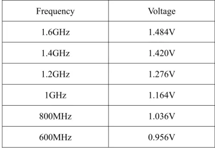
One kind of power management system is enhanced Intel SpeedStep technology. It is supported on current and future generations of Intel® Pentium® M processors. The Intel Pentium M processor at 1.6 GHz supports six frequency and voltage
Table 1.1 Performance states for the Intel® Pentium® M processor at 1.6GHz Frequency Voltage 1.6GHz 1.484V 1.4GHz 1.420V 1.2GHz 1.276V 1GHz 1.164V 800MHz 1.036V 600MHz 0.956V
In such application, dynamically control the system operating frequency, we will need a programmable, wide frequency range clock generator to provide various clock frequencies to confirm different work situations of the system.
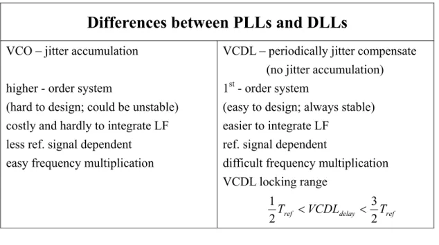
The clock generators could be solved by phase-lock loops (PLLs) or delay-locked loops (DLLs). There are some differences between PLLs and DLLs [8]. The VCO of PLLs will accumulate the phase errors induced by supply or substrate noise permanently. The VCDL of DLLs is triggered by a clean reference signal, so the phase noise accumulated in VCDL will be renewed by next reference signal edge. The phase noise accumulated only in one reference clock period. A DLL requires only one capacitor in its first-order loop filter. DLLs are more stable than higher order PLLs, and a PLL generally requires a more complex second-order filter. Second-order filter usually employs larger components which hardly to integrated. But the limited numbers of VCDL edges will make the DLLs hard to do frequency multiplication. Table 1.2 summarizes the differences between PLLs and DLLs.
Table 1.2 Differences between PLLs and DLLs.
Differences between PLLs and DLLs
VCO – jitter accumulation higher - order system
(hard to design; could be unstable) costly and hardly to integrate LF less ref. signal dependent
easy frequency multiplication
VCDL – periodically jitter compensate (no jitter accumulation) 1st - order system
(easy to design; always stable) easier to integrate LF
ref. signal dependent
difficult frequency multiplication VCDL locking range ref delay ref VCDL T T 2 3 2 1 < <
Because of low jitter performance, stability, and easy to design, so we prefer the DLLs to the PLLs.
To design a programmable, wide frequency range clock generator by the DLL, there are some issues must to solve, such as correct lock problem, limited locking range, and difficulty of frequency multiplication. When we use a DLL to provide frequency multiplication function, it generally need the DLL to lock in one reference period delay (normal locked state) to ensure the multiplied output frequency is desired. In order to lock in one reference period delay, the DLL’s locking range will be limited. If we want a DLL-based clock generator could provide wide output frequency range, we must to enlarge the DLL’s locking range. The multiplicity of output frequencies is determined by the numbers of multiplication factors. So, the multiplication method is one of the important design concerns of a DLL-based clock generator.
produced output frequency range can be wide. For multiplicity of produced clock, the clock generator needs more numbers of multiplication factors. With programmable property, when we vary the input frequencies and multiplication factors, the circuit expects to produce output frequency range from 100MHz to 1.6GHz.
1.2 Thesis Organization
Chapter 2 begins with the basics of the DLL-based clock generator and its operation. The details of the design challenges and review of the previous research is included in this chapter. In the end of this chapter, the design concepts in this project will be presented.
Chapter 3 begins with the introduction of DLL-based clock generator system. After that, the architecture of this project will be introduced. And the circuit block used in this architecture will also be described.
Chapter 4 presents the whole system’s simulation results. The measurement settings of the DLL-based clock generator and the measurement instruments are introduced. Then the measurement results of the prototype are shown.
Chapter 2
Design Challenges of DLL-Based Clock
Generator
This Chapter provides the fundamental knowledge of DLL-based clock generator which including the basics and the operation of the DLL-based clock generator. From the operation procedures, we can find the challenges of design this circuit. The details of the challenges and the design concepts are also presented in this chapter.
2.1 The Basics of the DLL-Based Clock Generator
The DLL-based clock generator takes advantage of the inherently low jitter of a low-frequency crystal oscillator reference to produce a low jitter multiplied output signal. This is accomplished by taking each relatively jitter-free but infrequent edge of the crystal oscillator output into delay line, and from the identical delay stages that generating a burst of well-controlled evenly spaced edges that span one period of the crystal oscillator. These evenly-spaced edges are combined to form a pattern of higher-frequency transition edges and eventually generate the desired output signal. Therefore, the jitter performance of the multiplied output signal is closely related to that of the reference crystal signal. This concept is shown in Fig. 2.1.
Unlike the conventional PLL-based clock generator, it uses VCO to generate the high-frequency output signal. The thermal-noise induced timing edge uncertainties accumulate over many reference clock cycles. The DLL-based clock generator, timing edge uncertainties accumulate within one period of the reference crystal, consequently the jitter does not increase within the crystal frequency. Given the extremely high Q and consequently very low jitter of the crystal oscillators, the jitter performance of the high-frequency output signal for this approach can be much lower than that of typical clock generator using integrated VCOs [4].
Fig. 2.1 DLL-based clock generator concept.
Because the output signal is produced by combine the VCDL output signals’ edges, and the numbers of delay stages is limited. So, the DLL-based clock generator is difficult to design the frequency multiplication.
2.2 The Operation of the DLL-Based Clock Generator
Fig. 2.2 is a conceptual block diagram of the DLL-based clock generator. The clock generator uses the DLL and edge combiner to produce the desired output signal.
The conventional DLL-based clock generator composed of a phase detector (PD), a charge pump (CP), a voltage-controlled delay line (VCDL), a loop filter (usually requires only one capacitor), and an edge combiner (EC).
Loop Filter Charge Pump Phase Detector
Voltage Control Delay Line
Ref Edge Combiner I II III IV V Ref I II III IV V Out
Fig. 2.2 Operation for DLL-based clock generator (ex: N=5)
The reference crystal signal is the input of the VCDL. Each delay element produces a delayed version of the reference crystal waveform. Because of the edge combine application, we hope the delay stages can be identical to each other. So, the VCDL in the DLL can generate N equal time-delayed output signals at the lock state of the DLL. The phase detector detects the phase difference between the input signal and the output signal of the delay line to generate an error signal. This error signal then is converted to charging or discharging current by the CP to charge or discharge the loop filter. The CP output is filtered by the loop filter and produces a voltage
signal Vc. The voltage signal Vc controls the VCDL to vary the delay time of each delay stage to minimize the phase error. When the loop is in the locked condition, the input and output of the delay line are in phase and the delay time is usually the reference signal period. The outputs of delay elements generate waveforms with edges that are evenly spaced within one period of the reference crystal [5].
The output waveform of the delay stage is the delayed-version of its input signal. When the DLL loop is in the locked state, the output of the last delay stage is in-phase with the reference crystal signal. So, the sum of the time delays from all delay stages is one period of the reference signal. In order to generate the high-frequency output signal, the edge combiner employs the outputs of the delay stages to produces the desired output signal. The system’s multiplication factor could be fixed or programmable, it determined by the architecture of the edge combiner. According to the multiplication factors which the edge combiner could be provide and the DLL operating frequency range, designers can determine the numbers of delay stages.
2.3 Design Challenges of DLL-Based Clock Generator
From the discussion of previous sections, we can understand the basics and the operation of the DLL-based clock generator. In order to apply to power management system, the clock generator will have some design challenges. First, to do a clock generator, the output clock frequency must be expected. The DLL loop must lock in one reference period delay and the delay stages will evenly distribute one reference period time. Then, Edge combiner using the VCDL outputs to generate the desired output signal. Second, for power management system, we hope the clock generator can provide more numbers of multiplication factors. More numbers of multiplication
factors the more steps of frequency adjustments can be. It will increase the power-save efficiency of the power management system. Final, the whole system may have many sub-systems which may work in the different operating frequencies depend on their operations. The power management system which has a wide-range clock generator can increases its usage extensively. The following sections will discuss the above challenges in detail and give the design concepts of this project.
2.3.1 Locking Issue
The conventional DLL may lock into three different states which are normal lock state, harmonic lock state, and stuck state, as shown in Fig. 2.3. The normal lock means the DLL-loop feedback signal is delayed one reference period, so the DLL lock in one reference period delay. The harmonic lock means the DLL-loop feedback signal is delayed two or more reference periods, so the DLL lock in integer multiples of reference periods delay. The stuck means the DLL feedback signal which want to trace the reference edge in the same period. But we know that the delay stages are never providing zero delay time. So, the delay stages always in the minimum delay state and the DLL stuck.
From the operation of DLL-based clock generator, we can know the system use edge combiner to combine the evenly spaced VCDL outputs to form the desired high-frequency signal. If the DLL lock in harmonic lock state, the evenly spaced VCDL outputs spans two or more periods of reference signal. In such situations, the output frequency of clock generator will be unexpected. So, we hope to control the DLL locked in the normal lock state.
Ref vcdl (correct_lock) Tref vcdl (correct_lock) vcdl (stuck) vcdl (harmonic_lock) correct lock range
Fig. 2.3 The locking states of the DLL.
From Fig. 2.3 and previous discussion of DLL lock conditions, we can know that the normal lock condition is the initial delay of the VCDL need to be located between 0.5 Tref and 1.5 Tref. As expressed as the following inequality:
ref VCDL ref T T T < ,min < 2 1 (2.1) ref VCDL ref T T T 2 3 max , < < (2.2)
Or, equivalently, in terms of Tref:
[
,min ,max]
max , min , 2 , 3 2 , VCDL ref VCDL VCDL VCDL T T Min T T T Max⎢⎣⎡ ⎥⎦⎤< < ⋅ (2.3)The available range is determined by inequality (2.3). If TVCDL,max ≥3⋅TVCDL,min, there is no range of Tref that satisfies the inequality, and the DLL is prone to the false locking problem. To avoid the false locking, TVCDL,max must be smaller than
min ,
3⋅TVCDL . So, the conventional DLL can not work without control circuit.
There are two methods to solve the DLL lock states issue. First method is built a lock detector circuit to detect the phase of VCDL outputs, and the detector will signal a message when the loops lock or false lock. If the detector must to detect a wide operating range, its design will be more complex. Moreover, it is hard to combine to DLL-based clock generator. Because the varieties of VCDL outputs selection is more complicated than application in simply DLL. Second method is built a startup circuit to set the initial conditions of the loop. The initial conditions let the loop in the correct locking range, such as the limitation given in equation (2.3). The startup circuit is suitable to combine with the DLL-based clock generator, and the area, power overhead is relatively low.
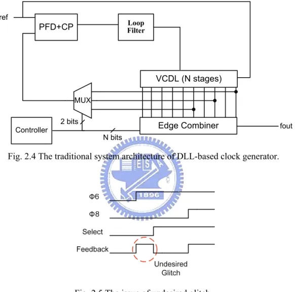
The traditional system architecture of the DLL-based clock generator is shown in Fig. 2.4. The operation of the system is the same as introduced in section 2.2. But, the project goal is design the clock generator has the programmable function and more numbers of multiplication factors. As discussion in section 2.2, we know that the last bit switching in VCDL can make different phase difference in each of the delay stage when DLL locked in correct lock state, and then input to the edge combiner, the system can produce more numbers of multiplication factors. To achieve the programmable function, designers can simply use the controller to control the edge
However, directly switching the last bit in VCDL will produce undesired glitch as shown in Fig. 2.5. The undesired glitch will confuse the PFD to produce extra up/down pulse, and may make the DLL fall into false lock condition.
PFD+CP FilterLoop
VCDL (N stages)
Edge Combiner fout
fref
MUX Controller
2 bits
N bits
Fig. 2.4 The traditional system architecture of DLL-based clock generator.
Fig. 2.5 The issue of undesired glitch.
2.3.2 Output Multiplied Issue
In the power management system, the more steps of frequency adjustments, the higher efficiency of the power-save performance. From the basics of DLL-based clock generator, we can know that the numbers of multiplication factors are depend on the numbers of delay stages. But, the intrinsic delay of the delay line will limit the
operating frequency of the DLL-loop, and its tuning range will determine the DLL operating range. It has the design trade-off between numbers of multiplication factors and the DLL operating frequency and its operating range.
Another factor which determines the numbers of multiplication factors is the architecture of edge combiner. Different Architecture of edge combiner has different operating principle and has different edge combine patterns. To decide clock generator’s hardware, we can start with the needs of frequency adjustments to determine an appropriate architecture of edge combiner. According to the numbers of multiplication factors which the combiner can provide to determine the numbers of delay stages of the DLL. In this section, according to the provided multiplication factors, we classify the architectures of edge combiner into three classifications, such as fixed multiplication, M to the power of N multiplication and N/2 scales multiplication.
Fixed multiplication
This type of edge combiner can provides only one multiplication factor of the output signal. The variety of the output clock frequency is only depending on the DLL’s operating frequency range. Because the architecture comprises LC-tank, so we called it, “LC-tank method” edge combiner.
To understand the operation of LC-tank edge combiner [4], [5], [16], we start from the analytical approach of the edge combiner. Since the edge combiner function is to sum the various delayed versions of the input signal, Vin, its operation is similar to a N-tap Finite Impulse Response (FIR) filter model. The five stage example is
shown in Fig. 2.6. Each “D” block represents a delay stage in the delay line, whose function is to delay the input signal, Vin, by 1 fc ( fc is the output carrier frequency). The output of the FIR filter can be shown in the following equation.
( )
j fo j fo j fo j fo outj
a
a
e
a
e
a
e
a
e
V
ω
ω ω ω 4 ω 4 3 3 2 2 1 0 − − − −+
+
+
+
=
(2.4)where ai are weighting coefficients in the digital filter. Assuming all the coefficients are unity, eq. 2.4 can be written as:
( )
j fo(
j fo j fo j fo j fo)
out
j
e
e
e
e
e
V
ω
=
−2 ω 2 ω+
ω+
1
+
− ω+
−2 ω(2.5) and can simplified to
( )
⎥
⎦
⎤
⎢
⎣
⎡
⎟⎟
⎠
⎞
⎜⎜
⎝
⎛
+
⎟⎟
⎠
⎞
⎜⎜
⎝
⎛
+
=
− o o f j outf
f
e
j
V
ω
2 ω o1
2
cos
ω
2
cos
2
ω
(2.6) The plot for eq. 2.6 is shown in Fig. 2.7 where the y-axis is the magnitude and the x-axis is frequency normalized to fo. The filter transfer function suggests that the DC and fo components are enhanced, where as the frequencies at integer multiples of5
0
f decay to zeros. For the DLL-based frequency multiplier, the harmonics of the reference input frequency are ideally cancelled with the exception at 5× fref
frequency, which is the desired output frequency in this example [5].
Fig. 2.7 Five-tap FIR filter transfer function.
Fig. 2.8 shows the circuit schematic for the edge combiner. The edge combiner is driven by the multi-phase outputs of the VCDL to produce the desired high-frequency signal. The differential pairs convert the voltage signals to the current signals and sum up at the differential output nodes. Two inductors are used to tune the output parasitic capacitance associated with the input differential pairs.
Iss
1p 1n 2p 2n 3p 3n 4p 4n 5p 5n
Out+
L
C
C
L
The drawbacks of the LC-tank edge combiner are the design flexibility and the cost. From the discussion of analytical approach of the edge combiner, we can see that the LC-tank edge combiner only can provide one multiplication factor. So, once the LC-tank values chosen, the multiplication factor is fixed. When design an N-times frequency multiplication function, N stages of delay line is decided. So, the design flexibility is low. Furthermore, use the L-component is occupied a large chip area and increases the cost.
M to the power of N multiplication
This type of edge combiner can provide several multiplication factors of the output signal. The scales of the multiplication factors are M to the power of N. M is determined by the function of edge combiner. N may be 0, 1, 2…, determined by the numbers of the multi-phase signals which input to the edge combiner. The variety of the output clock frequency is depending on the DLL’s operating frequency range and the numbers of the multiplication factors. There are two methods of this type edge combiner: AND-OR method and XOR method.
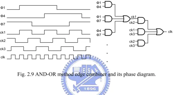
The AND-OR method edge combiner [6] and its phase diagram is shown in Fig. 2.9. This edge combiner is using the phase difference relations of each VCDL outputs to input the AND-OR gates to produce the multiplied output signal. The VCDL outputs φ1 ~φ9 are spans one reference period. If we put φ1, φ4, and φ7 into the first stage of AND-OR gates, it will produce the 3-times signal ck1. Equal to ck1, ck2 and ck3 are produced by put φ2, φ5, φ8 and φ3, φ6, φ9 into the first stage of AND-OR gates. To produce the 9-times signal clk, we can just put ck1, ck2, and ck3 into the second stage of AND-OR gates. Attach a controller, we can extract the 1x, 3x,
and 9x signal to as the final output signal and achieve the programmable function. From the discussion of the AND-OR method, we can know that this edge combiner can provides the three to the power of N multiplication function. When we try to achieve N=3, we will need 27 multi-phase signals, and it’s a very difficult mission. So it is appropriate to let N=2 and choice 9 delay stages of VCDL.
Φ1
.
.
.
Φ4 Φ1 Φ7 Φ4 Φ7 ck1 ck2 ck2 ck3 ck1 ck3 clk Φ1 Φ4 Φ7 ck1 ck2 ck3 clkFig. 2.9 AND-OR method edge combiner and its phase diagram.
The edge combiner with two to the power of N multiplication factors function is composed by the XOR gates [13], [20]. The simplified architecture is shown in Fig. 2.10. When the 90-degrees phase difference between the inputs of the XOR-gate, it can produce an output signal whose frequency is two-times of the input frequency. Consequently, we can use the 2-times frequency signals to produce the 4-times frequency signals and so on.
A B clk
A
B clk
The drawback of M to the power of N multiplication is the duty-cycle limitation of the input signals. From Fig. 2.9 and 2.10, we can see that the multiplication function only correct at 50% duty-cycle input signals condition. It needs some compensation for input signals, such as duty-cycle correction.
N/2 scales multiplication
This type of edge combiner [8], [17], [19] can provide N/2 scales multiplication. N is integer number controlled by the controller. The maximum value of N never exceed over the numbers of the multi-phase signals which input to the edge combiner. The variety of the output clock frequency is depending on the DLL’s operating frequency range and the numbers of the multiplication factors.
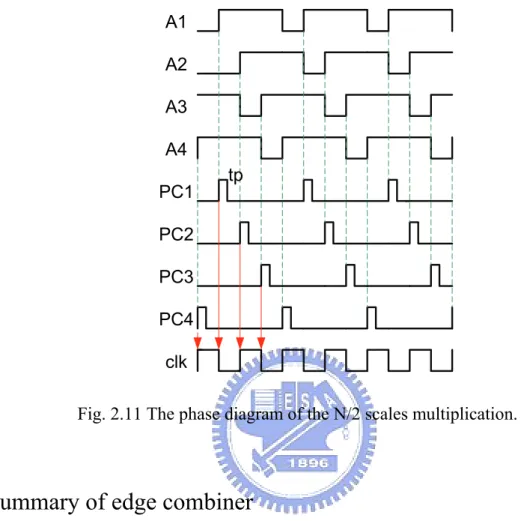
The operation of N/2 scales multiplication is shown in Fig. 2.11. Each Ai signal is the output of each delay stage. Whenever each multi-phase signal rises, we use a transition detector to generate a short period pulse signal PCi. The edge combiner puts the short pulses together and toggles the phase of output clk. Thus, the multiplied output clock signal toggles at every rising edge of signal Ai. Fig. 2.11 shows an example of frequency multiplication by two.
From the operation of this edge combiner and Fig. 2.11, we can see that even the input signals of the edge combiner not have 50% duty-cycle; it can produce a 50% duty-cycle clock signal. The limitation of input signals on M to the power of N methods edge combiner is vanished. Attach a controller; this type of edge combiner can easily to provide programmable function. Because N is determined by the numbers of multi-phase signals, and no limitation on input signals, the design
flexibility is better than previous two methods. A1 A2 clk A3 A4 PC1 PC2 PC3 PC4 tp
Fig. 2.11 The phase diagram of the N/2 scales multiplication.
Summary of edge combiner
The first approach, the LC-tank method edge combiner (fixed multiplication) is low design flexibility, and provides only one multiplication factor. Using L, and C components occupied large chip area and increases the cost.
The second approach, the AND-OR & XOR method edge combiner (M to the power of N multiplication) can attach a controller to produce programmable multiplication factors. The drawback of M to the power of N multiplication is the duty-cycle limitation of the input signals. The multiplication function only correct at 50% duty-cycle input signals condition.
The third approach, the pulse-toggle method edge combiner (N/2 scales multiplication) is high design flexibility, and no limitations on the inputs of the edge combiner. Attach a controller; it can program the multiplication factors easily. Consequently, this type of edge combiner is suitable to DLL-based clock generator in the application of power management system.
2.3.3 Wide Range Locking Issue
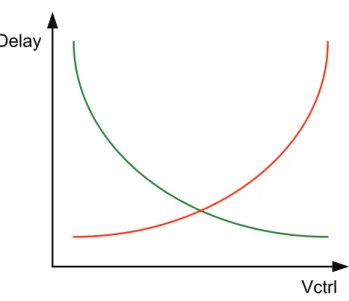
The possible transfer functions of VCDL are show in Fig. 2.12. Red line means the delay time of delay stage is direct proportion to the control voltage. On the contrary, green line means the delay time of delay stage is inverse proportion to the control voltage. The transfer functions of VCDL must be one of them. One control voltage corresponding to one delay time and than the DLL can trace one of the two lines to lock to the correct delay time. When DLL lock in a wide operating frequency, it means the VCDL must cover a wide delay range, and the control voltage on the LF must variation in a wide voltage range.
Delay
Vctrl
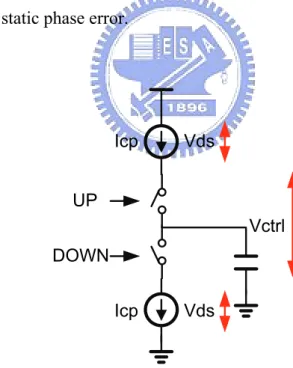
Fig. 2.13 shows the ideal charge pump(CP) and loop filter(LF), the up, down signals are the outputs of the phase frequency detector(PFD). The up and down signals control the switches, and let the charge or discharge current to charge or discharge the LF, and tune the delay time of the VCDL. From previous discussion, we know that the Vctrl will work in a wide voltage range. When the Vctrl varies, the Vds variation of up and down current MOS will vary in the opposite way, and the current mismatch of up and down current become large. If the DC gain from the PD to the LF is finite, a phase difference at inputs of the PD is required to sustain the desired control voltage. This phase difference is generally known as the static phase error. The CP current mismatch will bring about DLL system’s static phase error when DLL locked. We can see in the Fig. 2.14, the larger the CP current mismatch the more serious the system static phase error.
Icp Icp UP DOWN Vctrl Vds Vds
Fig. 2.14 The characteristic plot of PD.
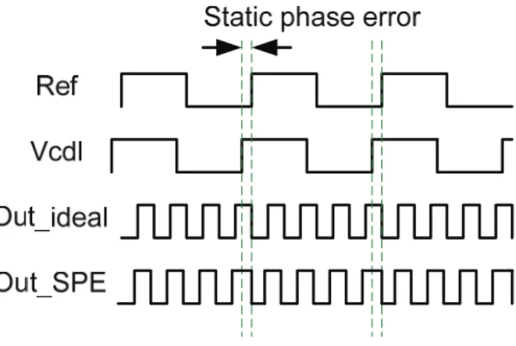
The static phase error in a DLL represents a phase difference between input and output waveforms of the delay line in a locked condition. The time domain effect of the static phase error is shown in Fig. 2.15. Because the synthesized output oscillations are triggered by the DLL output waveforms, an extended period is found at the end of each delay line cycle where the last oscillation completes and before the crystal reference starts the next cycle. The system static phase error will effects output signal performance and limit the DLL to work in a wide operating frequency range. The common way to minimize the static phase error is to make the DC loop gain as large as possible [5].
Fig. 2.15 Static phase error.
2.3.4 Project Design Concepts
The DLL-based clock generator applied in the power management system needs some properties such as wide output frequency range and multiplicity of the multiplication. When operating in a wide operating frequency range, designers must to overcome the locking state issue and static phase error issue. The multiplicity of the multiplication needs designers to determine which methods of multiplication and how many numbers of multiplication factors.
From previous discussion, we know that the lock detector is not suitable for the VCDL last bit switching application. In this project, we use the start up circuit proposed in [7] to set the system initial conditions for the DLL can always lock into correct lock state and widen the DLL operating range.
In order to produce more numbers of multiplication factors, we use the N/2 scales multiplication method edge combiner. The edge combiner proposed in [17] is suitable for the project. According to the switching patterns, we design a controller
blocks in the whole system. Attach a controller, this edge combiner can produce the output frequency Fout = (N/2) Fref. With different control patterns, N is programmable.
The static phase error in this project will be decrease by the action of pulse reshaper circuit proposed in [14]. The pulse reshaper circuit will change the characteristic plot of the PD-CP to decrease the system static phase error. Lighten the effect of static phase error; the clock generator can maintain the output signal performance even if the system operating frequency range is wide.
In the next chapter, we will introduce the system architecture and each block in detail.
Chapter 3
Target Circuit/System Introduction
This chapter starts from the introduction of the system architecture of DLL-based clock generator. After go through the system operation, we will see the details of every building block used in this project.
3.1 System Architecture
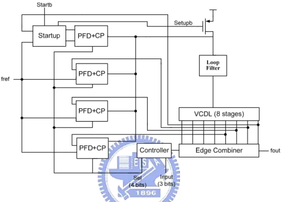
In Chapter 2, we know that the traditional architecture in Fig. 2.4 will produce the undesired glitch when VCDL last bit switching. The undesired glitch will make the PFD confused and let the system locked in the harmonic lock state. To overcome this issue, we use multi-PFD-CP pairs architecture proposed in [16]. The modified system architecture is shown in Fig. 3.1. When we fix the inputs of the PFD, the switching between PFD-CP pairs can achieve the last bit switching function and avoid the undesired glitch.
The operation of this architecture is as follow. The startup circuit set the initial conditions of the system to make the DLL lock in the correct lock state and widen the operating frequency range. PFD compares the phase difference of its inputs and sends the up/down signals to the CP. CP convert the voltage signals up/down to the current signal to charge or discharge the LF. The control voltage on LF is control the delay
and edge combiner to vary the multiplication factor. Edge combiner uses the evenly spaced multi-phase signals to produce the multiplied output signal. The detail of each block used in this architecture will discuss in following sections.
Fig. 3.1 The project system architecture of DLL-based clock generator.
3.2 Startup Circuit
The startup circuit proposed in [7] is used to overcome the lock states issue and widen the DLL operating frequency range. The startup circuit composed of two rising edge trigger DFFs, two NAND gates and two inverters. It receives three input signals: STARTB, REF, and VCDL and produces three output signals: SETUPB, OUT_REF, and OUT_VCDL. STARTB is the external signal to indicate when the system starts. REF is the external reference signal used in DLL operation. VCDL is the feedback signal in voltage control delay line. Initially, STARTB is set to low in order to clear the two DFFs’ outputs. Therefore, SETUPB is low and active the PMOS to pull the
control voltage to VDD as shown in Fig. 3.2. Because the VCDL delay time is inverse proportion to Vctrl, so the SETUPB initialize the VCDL delay to its minimum value.
DFF DFF Q REF STARTB Q D D clk clk SETUPB VCDL OUT_REF OUT_VCDL clr clr
Fig. 3.2 The architecture of startup circuit.
In the beginning, the OUT_REF and OUT_VCDL are in the low level. When STARTB goes to high, SETUPB will follow to high. After two consecutive falling edges of VCDL triggers the DFFs, the OUT_VCDL will be activated and input to the PFD to produce the down signal to discharge the LF, and increase the delay time of the delay stages. The delay will increase until the DLL lock in a reference period delay time. Attach a startup circuit, the delay stages work from the minimum delay to lock to one reference period delay time, the DLL will not fall into false lock even when 10TD,mun <0.5TREF. So, startup circuit also widens the operating frequency range of DLL system. Fig. 3.3 shows the simulation result of the startup circuit, the waveforms of the signals are consistent with the previous introduction.
Fig. 3.3 The simulation waveform of startup circuit.
3.3 PFD Circuit
The schematic of the PFD is shown in Fig. 3.4. Because of the PFD-CP pairs switching function, the PFD must have the enable/disable function. It is accomplished by add a NAND-gate on the feedback path. When enable is high, the positive-edge in either REF signal or VCDL signal, it will trigger to generate corresponding UP or DN signals. The UP or DN signals will send to the CP to produce the charge or discharge currents to the LF. On the other hand, if the enable signal is low, the PFD will not produce any output signals, even if the positive-edge of REF/VCDL is arrival. The simulation waveform is shown in Fig. 3.5. Both the UP and DN pulse generated, they will maintain the high level in a short time simultaneously to reduce the dead-zone of the PFD.
Fig. 3.4 The schematic of PFD circuit.
3.4 CP Circuit
The use of CP is to deposit or withdraw charges to the LF according to the phase difference determined by the PFD. This is accomplished by time-multiplexing charge pump currents in or out of the LF, and charges are deposited or withdrawn. The schematic of the CP is shown in Fig. 3.6. The reference current is produced from the left path, and uses the current mirror to mirror the current to the output node. All the switches are using the same type of MOS: PMOS. Because of the wide frequency range operation, the current mode CP circuit can suitable in the high speed operation. The simulation result is combining the PFD-CP to see the characteristic plot. From Fig. 3.7, we can see that the PFD dead-zone is less than 1ps.
Fig. 3.7 The characteristic plot of PFD-CP pair (simulation).
3.5 Pulse Reshaper Circuit
Review from Fig. 2.14, the current mismatch in CP currents will bring about the system static phase error when DLL in the lock condition. This will worsen the output clock signal performance. Unfortunately, when DLL lock in a wide operating frequency range, the control voltage on the LF must vary in a wide voltage range. Therefore, the CP currents mismatch is inevitable. In this project, we use the pulse reshaper circuit proposed in [14] to change the characteristic plot of PFD-CP pair, and reduce the system static phase error.
Fig. 3.8 shows the PFD with pulse reshaper circuit. The pulse reshaper circuit composed of two inverters and two AND gates. T means the masking window of m which delay is caused by low slew rate of the inverter. The timing diagrams are illustrated in Fig. 3.9. When DLL still unlock, the phase difference between REF and VCDL larger than T , only one RUP or RDOWN signal is at logic high, as Fig. m 3.9(c) shows. While the DLL in the lock state, there is no phase difference between REF and VCDL, both RUP and RDOWN are at logic high and go to logic low
difference less than T , the pulse RUP or RDOWN activated by the late clock has an m increasing voltage value like a glitch, as Fig. 3.9(b).
Fig. 3.8 The architecture of pulse reshaper circuit.
0 = −VCDL
REF REF−VCDL<Tm REF−VCDL>Tm
Fig. 3.9 The operation of pulse reshaper circuit.
The characteristic plot of PD attach a pulse reshaper can see the effect of reduce system static phase error. The plot is shown in Fig. 3.10. The little high gain range that cross the CP current mismatch line closer to the Y-axis, the static phase error will
also be reduced. This is because as phase difference of REF and VCDL is less than
m
T , the lagged signal produces a glitch-like RUP/RDOWN signal, so the difference of charge and discharge current will become larger. Therefore, when the slew of the inverter is almost linear, around the locking point (REF-VCDL <Tm), the voltage level of the reshaped pulse is inverse proportion to REF-VCDL , increases the gain slope of PD. The simulation result is composed of PFD, pulse shaper, and CP, shown in Fig. 3.11. π 2 _ × = period clock T M m
Fig. 3.10 The characteristic plot of PD with pulse reshaper circuit.
3.6 Delay Cell
In this project, we use the current-starved inverter type Delay cell to reduce the power consumption. The schematic is shown in Fig. 3.12. The delay cell comprises a single-ended inverter composed of M2 and M with series transistors 3 M1 and
4
M operating in the triode region. The delay time of delay cell is determined by the equivalent resistance of M1 and M4, controlled by V , controlled by the driving C transistors M and 7 M . An additional inverter which is 8 M and 5 M serves as an 6 output buffer which compensates the high frequency attenuation introduced by the preceding delay core. Moreover, the circuit performs a rail-to-rail operation, so it consumes no static power [16]. Because the numbers of delay stages will determine the delay range of the delay line. According to our design goals, we choose eight-stage delay line. We use the spice simulation to see the delay range of the delay cell, and it is shown in Fig. 3.13.
M4 Vout M3 M2 M1 M8 M7 M5 M6 Vin Vc VDD GND
Fig. 3.13 The simulation delay range of delay cell.
3.7 Edge Combiner
For power management application, the clock generator must have more numbers of multiplication factors. From chapter 2, we know the multiplication factor is determined by the architecture of the edge combiner. The pulse toggle method edge combiner can provides N/2 scales multiplication, so it is suitable in this project.
The architecture of the edge combiner proposed in [17] is shown in Fig. 3.14.
i
B signal is the output signals of the delay line, Si signal is control signal which determines the production of ki signal. If Bi signal rises, one input of a NAND gate will arrive faster than the other which comes after three-inverter delay. Therefore, at the rising edge of output of buffer, the NAND gate generates the negative narrow pulse ki corresponding to the three-inverter delay. Edge combiner uses the symmetric NAND gate and inverter to form the symmetric AND gate. Use three-stage of the symmetric AND gates to compose all the ki signals to form the A signal. The A signal pass to the TPL circuit to perform the divide-by-2 function, and produces the multiplied output clock signal. Because of the pulse-toggle method, the edge
have 50% duty-cycle. The pattern of the ki signals is in order to increases the operating frequency of the edge combiner. Because the transition overlap of the ki
signals may occur in three-stage of the symmetric AND gates. Because we use eight-stage delay line, so the edge combiner can provide 1/2, 2/2… 8/2, total eight multiplication factors which determined by the control signals. The simulation result is shown in Fig. 3.15. k1 B1 S1 k2 k8 B2 S2 B8 S8 k1 k5 k3 k7 k2 k6 k4 k8 x y i j A TPL dckb Q
Transition Detector Edge Combiner
mp
dckb dck
Q
Fig. 3.14 The architecture of edge combiner.
3.8 Controller
The system need to control the switching of multi-PFD-CP pairs and the edge combiner to determine the multiplication factor. The proposed control pattern is shown in Table 3.1. The pattern is in order to use the simplest logic gates to compose the controller. The numbers of 1 determined the N value which means the multiplication factor. Because the last 1 in Si must feedback to the PFD to compare phase difference with REF. So, the control signals of multi-PFD-CP pairs can also generate in this pattern.
Table 3.1 Project control pattern.
INPUTS OUTPUTS A B C S1 S2 S3 S4 S5 S6 S7 S8 0 0 0 0 0 0 0 0 0 0 1 0 0 1 0 0 0 1 0 0 0 1 0 1 0 0 1 0 1 0 1 0 0 0 1 1 0 1 0 1 0 1 0 1 1 0 0 1 1 1 1 1 0 0 0 1 0 1 1 1 1 1 1 1 0 0 1 1 0 1 1 1 1 1 1 1 0 1 1 1 1 1 1 1 1 1 1 1
Each control signal function is shown below: A S S S1 = 3 = 5 = , S2 =A+B, S4 =A+B+C, ACS6 =B+ , ABS7 =
(
A B)
BC S8 = + + , Enable8 = , S8 Enable7 =(
S7 +S8)
(
6 7 8)
6 S S S Enable = + + , Enable5 =(
S5 +S6 +S7 +S8)
The simulation results are shown in Fig.3.16.Fig. 3.16 The simulation result of controller.
If we don’t switch the last bit of delay line stages, the DLL’s feedback VCDL will not change, so it doesn’t need to relock. The system can changes the multiplication factor in only one cycle time. The simulation result is shown in Fig. 3.17.
Chapter 4
System Simulation Results and
Measurement Results
Each block of the project and simulation results are described in the previous chapter. In this Chapter, we introduce the simulation results of the DLL-based clock generator first. And follow by the measurement settings and the measurement results of the project.
4.1 System simulation results
In this project, the whole system simulation of DLL-based clock generator includes lock transient simulation, pulse reshaper effect on the static phase error, and the output signal transient waveform and jitter performance.
DLL Locked transient simulation
To generate the output clock signal, the DLL loop must lock in the correct lock condition first, and the each outputs phase of delay line will evenly space one reference period time. Than, according to the control signal, edge combiner will combine the multi-phase signals to produce the multiplied output signal. This project use the startup circuit to set the initial conditions of the system, the Vctrl will start from the VDD (delay line at the minimum delay state) and falling to the voltage that
delay time of the delay line just one reference period time. Fig. 4.1 shows the DLL lock in REF period 2.5ns, 3ns, and 4.2ns. In the three difference periods of REF, the DLL loop can always locked.
(a) REF_2.5ns
(b) REF_3ns
(c) REF_4.2ns
Pulse Reshaper Effect on the Static Phase Error
Fig. 4.2 shows the DLL locked static phase error difference between PFD with and without pulse reshaper circuit. Table 4.1 shows the performance of pulse reshaper.
(a) Without pulse reshaper
(b) With pulse reshaper
Fig. 4.2 Static phase error with and without pulse reshaper.
Table 4.1 Static phase error with and without pulse reshaper.
Tref Without pulse reshaper With pulse reshaper
2.5ns 183ps 23.8ps
3ns 74.3ps 6.4ps
Output Signal Transient Waveform
Fig. 4.3 shows the clock generator’s output waveform, the clock signal almost has 50% duty-cycle, consistent with the previous introduction of edge combiner.
(a) REF_2.5ns, multiplied by 4, Fout = 1.6GHz
(b) REF_3ns, multiplied by 4, Fout = 1.33GHz
(c) REF_4.2ns, multiplied by 4, Fout = 952MHz Fig. 4.3 Transient waveform of the output signal.
Output Signal Jitter Performance
Fig. 4.4 shows the clock generator’s output signal eye diagram, it can see the jitter performance of the output signal. Table 4.2 shows the jitter performance of output signal.
(a) REF_2.5ns, multiplied by 4, Fout = 1.6GHz Fig. 4.4 Jitter performance of the output signal.
(b) REF_3ns, multiplied by 4, Fout = 1.33GHz
(c) REF_4.2ns, multiplied by 4, Fout = 952MHz Fig. 4.4 Jitter performance of the output signal.
Table 4.2 Jitter performance of output signal.
Tref Fout Jitter 2.5ns 1.6GHz 22ps
3ns 1.33GHz 23ps 4.2ns 952MHz 42ps
Post-Layout Simulation
After the pre-layout simulation to confirm the function of the project, we start to draw the layout of the project and tape-out to generate the chip. The post-layout simulation is show in Fig. 4.5; it includes lock transient, static phase error, output waveform and output eye diagram.
(a) REF_3ns Vctrl transient.
(b) REF_3ns static phase error.
(c) REF_3ns, multiplied by 4, Fout = 1.33GHz
(d) REF_3ns, multiplied by 4, Fout = 1.33GHz
Fig. 4.5 Post-layout simulation of the DLL-based clock generator.
Layout and Performance Summary
The layout of the designed DLL-based clock generator is show in Fig. 4.6. The whole chip occupies an area of 0.65×0.76mm2. The performance summary of the
project is listed in Table 4.3. The jitter of the output signal is worse than pre-layout simulation. It is because the careless of the loading match between each delay stage.
In the static phase error aspect, the post-layout simulation still shows the good performance.
Table 4.3 Performance summary.
Pre-sim Post-sim
Operating Frequency Range 200MHz~450MHz 200MHz~400MHz Output Frequency Range 100MHz~1.8GHz 100MHz~1.6GHz
Static Phase Error
12ps @ REF_2.7ns 6.4ps @ REF_3ns 1.6ps @ REF_4.2ns -5.5ps @ REF_2.7ns -2.5ps @ REF_3ns 13ps @ REF_4.2ns Peak-to-Peak Jitter 42ps @ 952MHz 22ps @ 1.33GHz 13ps @ 1.48GHz 76ps @ 952MHz 70ps @ 1.33GHz 64ps @ 1.48GHz Lock Time ~200ns ~250ns Power Dissipation 25.88mW @ 1.33GHz 26.36mW @ 1.33GHz Layout Area N/A 0.65×0.76mm2
4.2 Measurement Settings
The clock generator receives reference signal to generate multiplied output signal. The jitter performance of the output signal is measured at the oscilloscopes shown in Fig. 4.7(a). In a DLL-based clock generator, a reference pulse signal is critical, and such signal is generated by pulse generator shown in Fig. 4.7(b).
Fig. 4.7 The photograph of the (a) oscilloscopes TDS7704B, (b) pulse generator Anritsu MP1763C.
The prototype PCB is shown in Fig. 4.8. The chip is measured by a chip on PCB assembly and the measurement environment is setup as Fig. 4.9. The control signals are produced by the switches made on PCB. An on chip open drain buffer delivers the output signal through the bias-Tee to the oscilloscopes.
Fig. 4.8 Prototype PCB.
Fig. 4.9 Measurement setup.
4.3 Measurement Results
The wide-range, programmable DLL-based clock generator has been fabricated in a 0.18-μm CMOS technology. Fig. 4.10 is a photograph of the die, whose area is 0.65mm by 0.76mm. The measurement results are presented in the following.
Fig. 4.10 The photograph of the die.
The measurement operating frequency range is from 200MHz to 400MHz, the results are shown in Fig. 4.11 to Fig. 4.13. The measurement results show that the designed clock generator can generates three numbers of multiplication factors, such as 1/2, 1, and 4. When operating in multiplied by 4 mode, the device’s maximum output frequency is 1.2GHz, the peak to peak jitter is 128ps, and the power consumption is 63mW (whole power). The summary of measurement results is shown in Table 4.4.
There are five numbers of multiplication factors can not be produced. This is caused by the fail detection of the PFD. PFD detects the rising edges of reference
signal and feedback signal. But designed enable function of PFD is just control the feedback path of PFD to disable the PFD operation. Therefore, when the PFD be enable after the rising edge of reference signal or feedback signal, there will miss one pulse of up or down message. This phenomenon will make the DLL loop fall into false locking situation and produce the unexpected output signal.
Fig. 4.11 Waveform of the output signal, REF = 200MHz (a) multiplied by 1/2 and (b) multiplied by 1
Fig. 4.12 Waveform of the output signal, REF = 400MHz (a) multiplied by 1/2 and (b) multiplied by 1
Fig. 4.13 Waveform of the output signal, REF = 300MHz (a) multiplied by 1/2, (b) multiplied by 1 and (c) multiplied by 4
Table 4.4 Measurement summary.
Post-sim Measurement Operating frequency range 200MHz ~ 400MHz 200MHz ~ 400MHz
Output frequency range 100MHz ~ 1.6GHz 100MHz ~ 1.2GHz Peak-to-peak jitter 0.7ps @ 300MHz 1ps @ 400MHz 73ps @ 1.2GHz 50ps @ 300MHz 40ps @ 400MHz 128ps @ 1.2GHz
Lock time ~250ns N/A
Power dissipation 40.3mW @ 1.2GHz 63mW @ 1.2GHz Layout area 223um*280um 223um*280um
Chapter 5
Conclusion and Future Works
5.1 Conclusion
In this thesis, a programmable, wide-range DLL-based clock generator is presented. The design challenges of this project such as lock issue, output multiplied issue, and wide-range lock issue are discussed. Multi-PFD-CP pairs structure with startup circuit, make the system can produce more numbers of multiplication factors and avoid the undesired glitch when DLL-loop feedback signal switching. Attach pulse reshaper circuit, the static phase error of DLL can be reduced and the jitter performance of output signal can maintain its level in a wide operating range. Finally, the designed DLL-based clock generator is implemented.
Measurement results show that the designed clock generator can work in three multiplication factors, such as 1/2, 1, and 4. With different control pattern, the DLL-based clock generator can produce the frequency ranging from 100MHz to 1.2GHz. The jitter is 128ps at 1.2GHz. The chip size is 0.65×0.76mm2. The power
consumption of the DLL is 63mW under 1.8V power supply. The designed DLL-based clock generator is fabricated in TSMC 0. 18 μm CMOS process.
5.2 Future Works
In this project, we use multi-PFD-CPs architecture to achieve the DLL feedback signal switching function without the production of undesired glitch. But the increased three PFD-CP pairs occupied ~30% of the active area. If we can design a detector to replace the function of multi-PFD-CPs architecture, we can reduce an appreciable active area.
The following project in our LAB is already design such a detector in DLL-based clock generator. With the detection circuit, the new clock generator can produce the entire multiplication factors, and the active area is 0.18×0.22mm2. The
new version of the clock generator is reducing 37% active area compared to this clock generator.
The power consumption of the edge combiner is almost half of the total power. If we can active the edge combiner when the DLL is already lock, we can reduce the power consumption of the system. It may be next generation of the clock generator in the design road map.
Reference List
[1] J. G. Maneatis, “Low-jitter process-independent DLL and PLL based on self-biased techniques,” IEEE J. Solid-State Circuits, pp. 1723-1732, Nov. 1996. [2] Y. Moon, J. Choi, K. Lee, D. –K. Jeong, and M. –K. Kim, “An all-analog
mul-tiphase delay-locked loop using a replica delay line for wide-range operation and low-jitter performance,” IEEE J. Solid-State Circuits, pp.377-384, Mar. 2000. [3] G. –K. Dehng, J. –M. Hsu, C. –Y. Yang, and S. –I. Liu, “Clock-deskew buffer
using a SAR-controlled delay-locked loop,” IEEE J. Solid-State Circuit, vol. 35, pp. 1128-1136, Aug. 2000.
[4] G. Chien, and P. R. Gray, “A 900MHz local oscillator using a DLL-based frequency multiplier technique for PCS applications,” IEEE J. Solid-State Circuits, pp. 1996-1999, Dec. 2000.
[5] G. Chien, “Low-noise local oscillator design techniques using a DLL-based frequency multiplier for wireless application,” University of California, Berkeley, PhD Thesis, Spring 2000.
[6] D. J. Foley and M. P. Flynn, “CMOS DLL-based 2-V 3.2-ps jitter 1-GHz clock synthesizer and temperature-compensated tunable oscillator,” IEEE J. Solid-State Circuits, pp. 417-423, Mar. 2001.
[7] H.-H. Chang, J.-W. Lin, C.-Y. Yang, and S.-I. Liu, “A wide-range delay-locked loop with a fixed latency of one clock cycle,” IEEE J. Solid-State Circuits, pp. 1021-1027, Aug. 2002.
[8] C. Kim, I.-C. Hwang, and S.-M. Kang, “A low-power small-area 7.28-ps-jitter 1-GHz DLL-based clock generator,” IEEE J. Solid-State Circuits, pp. 1414-1420, Nov. 2002.
[9] R. Farjad-Rad, W. Dally, H.-T. Ng, R. Senthinathan, M.-J. E. Lee, R. Rathi, and J. Poulton, “A low-power multiplier DLL for low-jitter multigigahertz clock generation in highly integrated digital chips,” IEEE J. Solid-State Circuits, pp. 1804–1812, Dec. 2002.
[10] M. –J. Edward Lee, W. J. Dally, T. Greer, H. –T. Ng, R. Farjad-Rad, J. Poulton, and R. Senthinathan, “Jitter transfer characteristics of delay-locked loops – theories and design techniques,” IEEE J. Solid-State Circuit, pp. 614-621, Apr. 2003.
[11] J. Zhuang, Q. Du, and T. Kwasniewski, “A -107dBc, 10kHz carrier offset 2-GHz DLL-based frequency synthesizer,” IEEE Custom Integrated Circuits Confs., pp. 301-304, Sep. 2003.
[12] K. H. Cheng, S. M. Chang, Y. L. Lo, and S. Y. Jiang, “A 2.2 GHz programmable DLL-based frequency multiplier for SOC applications,” IEEE Asia-Pacific Conference on Advanced System Integrated Circuits, pp. 72-75, Aug. 2004. [13] K.-H. Cheng, S.-M. Chang, S.-Y. Jiang, and W.-B. Yang, “A 2GHz fully
differential DLL-based frequency multiplier for high speed serial link circuit,” IEEE International Symposium on Circuits and Systems, pp. 1174-1177, May. 2005.
[14] B.-G. Kim, and L.-S. Kim, “A 250-MHz-2-GHz wide-range delay-locked loop,” IEEE J. Solid-State Circuits, pp. 1310-1321, Jun. 2005.
[15] P. Torkzadeh and A. Tajalli and M. Atarodi, “A wide tuning range, 1GHz-2.5GHz DLL-based fractional frequency synthesizer,” in IEEE
[16] T.-C. Lee, and K.-J. Hsiao, “The design and analysis of a DLL-based frequency synthesizer for UWB application,” IEEE J. Solid-State Circuits, pp. 1245-1252, Jun. 2006.
[17] J.-H. Kim, Y.-H. Kwak, M. Kim, S.-W. Kim, and C. Kim, “A 120-MHz-1.8-GHz CMOS DLL-based clock generator for dynamic frequency scaling,” IEEE J. Solid-State Circuits, pp. 2077-2082, Sep. 2006.
[18] Q. Du, J. Zhuang, and T. Kwasniewski, “A low-phase noise, anti-harmonic programmable DLL frequency multiplier with period error compensation for spur reduction,” IEEE Transaction on Circuit and Systems, pp. 1205-1209, Nov. 2006.
[19] Ro-Min Weng, Chun-Yu Liu, Ming-Hui Liang, and Yue-Fang Kuo, “A 192MHz to 1.946GHz programmable DLL-based frequency multiplier for RF application,” IEEE International Conference on Consumer Electronics, pp. 1-2, Jan. 2007.
[20] Chih-Hsing Lin; Ching-Te Chiu, “A 2.24GHz wide range low jitter DLL-based frequency multiplier using PMOS active load for communication applications,” IEEE International Symposium on Circuits and Systems, pp. 3888-3891, May 2007.
[21] K. Chung, J. Koo, S.-W. Kim, and C. Kim, “An anti-harmonic, programmable DLL-based frequency multiplier for dynamic frequency scaling,” IEEE Asian Solid-State Circuits Conference, pp. 276-279, Nov. 2007.
[22] Faisal, M.; Bayoumi, M.A. “A low-area, low-power programmable frequency multiplier for DLL based clock synthesizers,” IEEE International Symposium on Circuits and Systems, pp. 1460-1463, May 2008.
[23] “Enhanced Intel speedstep technology for the Intel Pentium M processor,” Intel white paper, March 2004.