針對安全性嵌入式系統之彈性管線化設計與實做
Design and Implementation of a Flexible Pipeline for Secure
Embedded Systems
研 究 生:陳 治 瑋 Student:Zhi-Wei Chen
指導教授:單 智 君 博士 Advisor:Dr. Jean, Jyh-Juin Shann
國 立 交 通 大 學
資 訊 工 程 學 系
碩 士 論 文
A Thesis
Submitted to Department of Computer Science and Information Engineering
College of Electrical Engineering and Computer Science
National Chiao Tung University
in Partial Fulfillment of the Requirements
for the Degree of
Master
In
Computer Science and Information Engineering
June 2004
Hsinchu, Taiwan, Republic of China
具安全考量之嵌入式系統的彈性管線化設計與實做
學生:陳治瑋 指導教授:單智君 博士 國立交通大學資訊工程學系(研究所)碩士班摘 要
在現今的環境中,提供加密的需求已是刻不容緩,如果在嵌入式系統中加入加密 的運算,就會遇到幾項議題,其中我們針對處理速度以及硬體彈性這兩項議題進行討 論,我們針對目前較常見的加密演算法,分別為 AES DES 和 RSA。提供一個可在 AES,DES 和 RSA 之間彈性轉換,並且可以彌補速度上不足之硬體。在考量處理速 度不足這項議題之下,我們採用速度與面積乘積為評比標準。 在本論文中,我們首先分析此三演算法之運算需求,然後針對不同類型之運算分 別設計出排列組合單元,運算單元以及記憶單元,其中排列組合單元採客制化設計, 運算單元由處理單元所組成,記憶單元則由單位緩衝區所組成,我們討論處理單元以 及單位緩衝區的設計以及考量在不同比例之運算單元以及單位緩衝區之下,造成面積 速度乘積的影響,最後所提出的設計和針對個別演算法之客制化設計做比較,比較結 果顯示我們的方法確實在面積速度乘積有較好的效果。Design and Implementation of a Flexible Pipeline for Secure
Embedded Systems
Student:ZhiWei Chen Advisor:Dr, Jean, J.J Shann
Institute of Computer Science and Information Engineering National Chiao-Tung University
Abstract
Providing security has become more and more urgent and necessary in embedded systems. If we want to support security in our embedded systems, some issues must be solved. We focus on processing gap and flexibility concerns. We target on the three commonly used cryptographic algorithms, AES, DES and RSA. In our thesis, we want to propose a hardware which solves the processing gap and switches flexibly between AES, DES, and RSA. Under the consideration of processing gap, we use space-time product as our performance metrics.
We first classify the operation of the three cryptographic algorithms into three classes. Then, we design modules for different operation classes respectively. The three modules are permutation-combination unit, computation unit and memory unit. The permutation-
combination unit is a custom design. The computation unit is consisted of processing elements and the memory unit is consisted of tile buffers. The different ratio of processing elements and tile buffers will lead to different results. We choose the most appropriate ratio. Finally, our proposed method will get better result than ASIC design.
誌 謝
首先感謝我的指導老師 單智君教授,在老師的諄諄教誨、辛勤指導與勉勵下, 我得以順利完成此論文,並且順利通過畢業口試。同時感謝我的口試委員 鍾崇斌教 授以及謝萬雲教授,由於他們的指導與建議,讓這篇論文更加完整和確實。 此外,感謝實驗室的學長—蔣昆成學長和喬偉豪學長,每次都不厭其煩地跟我討 論許多問題,還帶我去吃海鮮,給予我莫大的幫助。也感謝實驗室全體學長姐、同學 以及學弟們,真的很高興可以認識你們大家。因為你們,讓我的研究生活充滿了歡樂 跟 dota。 最後感謝我的家人,謝謝你們在背後全心全意地支持我,讓我在這研究的路上走 得更順利,進而能無後顧之憂的學習,讓我追求自己的理想。 謹向所有支持我、勉勵我的師長與親友,奉上最誠摯的祝福,謝謝你們。 陳治瑋 2005. 8. 15Table of contents
中文提要 ……… ii
英文提要 ……… iii
誌謝 ……… iv
Table of contents ……… v
List of Figures ……… viii
List of Tables ……… xi
1 Introduction ……… 1
1.1 Design Challenges of Secure Embedded Systems ……… 2
1.1.1 Processing Gap ……… 2
1.1.2 Flexibility Concerns ……… 3
1.2 Architecture for Security Processing ……… 5
1.3 Motivation and Objective ……… 6
2 Background and Related Work ……… 8
2.1 Overview of Cryptography ……… 8
2.2 Symmetric and Asymmetric Cryptosystems ……… 9
2.3 AES ……… 11 2.3.1 Definition ……… 12 2.3.2 Key Expansion ……… 12 2.3.3 SubBytes ……… 13 2.3.4 ShiftRows ……… 14 2.3.5 MixColumn ……… 15
2.3.6 Add Round Key ……… 17
2.4 DES ……… 17 2.4.1 Permutations ……… 18 2.4.2. Round ……… 20 2.5 RSA ……… 21 2.5.1 RSA Components ……… 21 2.5.2 Complexity of RSA ……… 22
2.5.3 Fast Exponentiation Algorithm ……… 22
2.5.4 Montgomery Algorithm ……… 24
2.6 Some Hardware Implementations ……… 26
2.6.1 Integrated Design ……… 27
2.6.2 Dedicated Design ……… 29
3 Design ……… 33
3.1 Function Requirement ……… 33
3.2 System Overview ……… 35
3.3 Permutation and Combination Unit ……… 37
3.4 Computation Unit ……… 37
3.4.1 Observation ……… 37
3.4.2 Organization of Computation Unit ……… 39
3.4.3 Design of P.E ……… 40
3.4.4 Additional hardware for MON ……… 48
3.5 DES Unit ……… 48
3.6 Memory Unit ……… 49
3.6.1 Organization ……… 49
3.6.2 Preload Buffer ……… 50
3.6.3 Ratio of PE and Tile Buffer ……… 51
3.7 Context Memory and Context Decoder ……… 55
3.8 CTRL ……… 56 4 Evaluation Results ……… 58 4.1 Evaluation Environment ……… 58 4.2 Processing Gap ……… 58 4.3 ASIC ……… 59 4.3.1 AES ……… 59 4.3.2 DES ……… 60 4.3.3 MON ……… 61 4.3.4 ASIC Summery ……… 62
4.4 Proposed approach ……… 62
4.5 Timing and Area ……… 63
4.6 Space-time product ……… 64
4.6.1 Stand alone design ……… 65
4.6.2 Take off SRAM ……… 66
4.7 Summary ……… 67
5 Conclusion and Future work ……… 68
5.1 Conclusion ……… 68
List of Figures
Fig. 1-1 Obstacles preventing consumers from adopting Mobile Commerce …… 1
Fig. 1-2 Throughput of high and low end embedded processors ……… 2
Fig. 1-3 Evolution of security protocols ……… 4
Fig. 1-4 Security processing architectures ……… 6
Fig. 2-1 Typical cripto algorithm block diagram ……… 9
Fig. 2-2 Public Key Cryptosystem ……… 10
Fig. 2-3 Flow of AES ……… 11
Fig. 2-4 4 Key Expansion Flow ……… 13
Fig. 2-5 SubBytes applies Sbox to each byte of the state ……… 13
Fig. 2-6 SubBytes transformation ……… 14
Fig. 2-7 shift cyclically the state ……… 14
Fig. 2-8 Mixcolumn ……… 15
Fig. 2-9 X_TIME ……… 15
Fig. 2-10 Data flow graph of encryption and decryption ……… 16
Fig. 2-11 Add Round Key ……… 17
Fig. 2-12 Flow of DES ……… 17
Fig. 2-13 Organization of Round ……… 20
Fig. 2-14 Flow of RSA ……… 23
Fig. 2-15 Modified RSA flow ……… 26
Fig. 2-16 Cryptonite Architecture ……… 27
Fig. 2-17 ALU of Cryptonite ……… 28
Fig. 2-18 Organization of 15] ……… 30
Fig. 2-19 The new DES pipeline ……… 31
Fig. 3-1 System overview ……… 35
Fig. 3-2 En/Decryption data flow graph of Mixcolume and AddroundKey ……… 38
Fig. 3-3 MON data flow graph ……… 38
Fig. 3-4 Granularity of the two cryptographic algorithms ……… 39
Fig. 3-5 Organization of CU ……… 39
Fig. 3-6 Partition AES and MON ……… 41
Fig. 3-7 OP set for OPSET 1 ……… 41
Fig. 3-8 OPSET 1 organization ……… 41
Fig. 3-9 Partition AES and MON ……… 42
Fig. 3-10 OP set for OPSE 2 ……… 42
Fig. 3-11 OPSET 2 organization ……… 42
Fig. 3-12 Partition AES and MON ……… 43
Fig. 3-13 OP set for OPSET 3 ……… 43
Fig. 3-14 OPSET 3 organization ……… 43
Fig. 3-15 Partition AES and MON ……… 44
Fig. 3-16 OP set for OPSET 4 ……… 44
Fig. 3-17 OPSET 4 organization ……… 44
Fig. 3-18 AES space time product of the four OPSETs ……… 46
Fig. 3-19 MON space time result of the four candidates ……… 46
Fig. 3-20 Space time result of the four OPSET ……… 47
Fig. 3-21 Organization of PE ……… 47
Fig. 3-22 Additional hardware ……… 48
Fig. 3-23 Organization of DES unit ……… 49
Fig. 3-24 Organization of MU ……… 50
Fig. 3-26 Space time product of different ratio in AES ……… 52
Fig. 3-27 Space time product of different ratio in symmetric cryptography … 53 Fig. 3-28 Space time product of asymmetric cryptography……… 53
Fig. 3-29 Space time product of total result……… 54
Fig. 3-30 System overview ……… 54
Fig. 3-31 Organization of Context Decoder ……… 55
Fig. 3-32 Finite state machine of CTRL ……… 57
Fig. 4-1 Throughput of proposed design ……… 59
Fig. 4-2 ASIC of AES ……… 59
Fig. 4-3 ASIC of DES ……… 60
Fig. 4-4 ASIC of MON ……… 61
Fig. 4-5 Proposed approach ……… 62
Fig. 4-6 Area result of stand along design ……… 64
Fig. 4-7 Area result of stand along design ……… 64
Fig. 4-8 Symmetric cryptography result……… 65
Fig. 4-9 Asymmetric cryptography result……… 65
Fig. 4-10 Result of symmetric and asymmetric cryptography ……… 65
Fig. 4-11 Symmetric cryptography result ……… 66
Fig. 4-12 Asymmetric cryptography result ……… 66
Fig. 4-13 Result of symmetric and asymmetric cryptography ……… 55
Fig. A-1 Symmetric result ……… 73
Fig. A-2 Asymmetric result ……… 73
Fig. A-3 Total result ……… 74
List of Tables
Table 2-1 Key Block Round Combination ……… 12
Table 2-2 Xi of Rcon[i] ……… 12
Table 2-3 Shift number C1 means Column one ……… 14
Table 2-4 Left shifts number ……… 18
Table 2-5 Comparison of Cryptonite and proposed design ……… 29
Table 2-6 Comparison of AES ASIC ……… 30
Table 2-7 Comparison of DES ASIC ……… 31
Table 2-8 Comparison of RSA ASIC ……… 32
Table 3-1 Function requirements ……… 33
Table 3-2 Operation classification ……… 34
Table 3-3 Permutation and combination performed by PCU ……… 37
Table 3-4 Hardware requirements of the three cryptographic algorithms … 37 Table 3-5 Area and timing of the four OPSET ……… 45
Table 3-6 Cycles needed by different specification of cryptographic algorithms ……… 45 Table 3-7 Bandwidth requirements for three cryptographic algorithms ……… 51
Table 3-8 Area of PE and Tile Buffer ……… 52
Table 4-1 Processing Gap of secured embedded system ……… 58
Table 4-2 Area or timing of each component in AES ASIC ……… 60
Table 4-3 Area or timing of each component in DES ASIC ……… 61
Table 4-4 Area or timing of each component in RSA ASIC ……… 61
Table 4-5 Area timing and cycles of the three ASIC respectively ……… 45
Table 4-6 Area and timing of each component in modified approach ………… 63
國
立
交
通
大
學
資訊工程系
碩
士
論
文
針對安全性嵌入式系統之彈性管線化設計與實做
Design and Implementation of a Flexible Pipeline for Secure
Embedded Systems
研 究 生:陳 治 瑋
指導教授:單 智 君 博士
Chapter 1 Introduction
Curiosity about other people's business and the hiding of information are characteristic of all human societies. In military, commerce, and diplomat, protecting some confidential papers is more and more important. Furthermore, embed security feature in some personal devices, such as PDA and handset, has become a considerable factor for consumers. According to the statistic of Mobile Commerce taken by ePaynews.com, nearly 52% of cell phone users and 47% of PDA users feel that security is the largest concern preventing the adoption of Mobile Commerce. The statistic bar graph is shown in Fig.1-1. In the Fig. 1-1, the second important reason is the klunky user experience. It means the habits of experienced users. The two reasons account for 70% of the statistics. [1]
Besides the urgent necessity, the stronger computing power and the more impeccable development of mathematical techniques have make cryptosystems extremely sophisticated. It's able to construct ciphers that are effective and impossible to break. As a result, embedded systems adapt some security features is necessary and possible.
0% 10% 20% 30% 40% 50% 60%
Credit card security concerns
Fear of 'klunky' user experience
Don't understand how it would work
Other Never heard of it before
Phones PDAs
1.1 Design Challenges of Secure Embedded Systems
Many embedded systems are constrained by the environments they operate in, and by the resources they possess. For secure embedded systems, there are some new design challenges. These new design challenges are processing gap, flexibility concerns, battery gap, tamper resistance, assurance gap and cost. The processing gap means the gap between bandwidth of devices and environments. The flexibility concerns come from the characteristics of cryptographic algorithms. Battery gap is the insufficiency of battery. The tamper resistance is the countermeasure for malicious software such as viruses and Trojan horses. The assurance gap is the gap between current systems and the reliable systems which never crash under any kind of situation. Last but not least, the cost is the area constrain of embedded environment. [2] Our thesis is focus on processing gap and flexibility concerns.
1.1.1 Processing Gap
At different environments, data rates of cellular (128 kbps~2Mbps), wireless Lan (2~60Mbps) and the lower-end of access network (~100Mbps) are supported by current low- and high-end embedded processors. [2] Take XScale as an example, when it 100% dedicates for record protocol of Secure Socket Layer (SSL) which is a popular security protocol, it can only sustain data rate 3.1Mbps. Any higher rates are unattainable. If we use this embedded process for SSL, this would lead processing gap. In Fig.1-2 shows the throughput of low- and high-end processors. The horizontal axis is MIPS of embedded processors. The vertical axis is data rate produced by these embedded processors. We choose some popular processor. For low-end system, we choose the XScale, ARM9 and SA-1110 as an example. For high-end system, we choose Xcon and PIII.
Fig. 1-2 Throughput of high- and low- end embedded processors [2]
1.1.2 Flexibility Concerns
A typical security protocol standard usually allows for a wide range of cryptographic algorithms. In general, asymmetric cryptographic algorithms are used to exchange the keys which needed by symmetric ones. If we use ASIC to speed up the two cryptographic algorithms individually, hardware utilization will be very low. The low utilization comes from using symmetric and asymmetric ASIC in sequence. When we use asymmetric cryptographic algorithms to exchange keys, the hardware used to speed up symmetric
cryptographic algorithms is idle. It is the same for asymmetric ones when symmetric ones are active.
Fig. 1-3 Evolution of security protocols [2]
Besides the requirement of supporting different cryptographic algorithms, security protocols and cryptographic algorithms are not only diverse, but also continuously evolving over time. As time goes by, future computation power will become stronger than current one. The current cryptosystem will become insecurity. So, we need some new cryptographic algorithms or some cryptographic enhancements. As the Fig.1-3 shows, these security protocols add more and more features from 1990 to 2002. For cryptographic algorithms itself, take DES as an example. 3DES is an enhancement algorithm with respect to DES. It uses the same cryptographic algorithm, but need longer key to support higher security level.
As a result, embedded systems supporting for security need some kinds of flexibility concerns between different cryptographic algorithms and forward compatible for future ones.
1.2 Architecture for Security Processing
As the security embedded systems grow, there are two generations of security processing architecture. The First-generation solutions perform security processing by executing security software on the embedded processors. Because they use software to perform cryptographic algorithms, they have high flexibility and fast turn around time. Unfortunately, the characteristic of processor which is designed to execute any kind of application leads doesn’t meet the case for stream data processing. The most execution time is spent on instruction fetch and decode. Nevertheless, the applications such like cryptographic algorithms are fixed. As a result, the First-generation solutions are not efficient in terms of their performance and energy consumption.
The First-generation solutions have the defect of performance. Some people suggest that design a dedicated hardware to speed up cryptographic algorithms. It is a good approach in the view point of processing gap. So, the Second-generation solutions are proposed. The Second-generation ones sacrifice the flexibility and turn around time. The benefits of them are hardware efficiency and low power. These advantages are due to the custom design. But, as the section 1.1 tells us, the cryptographic algorithms are not only diverse, but also continuously evolving over time. As time goes by, the mainstream cryptographic algorithms may be replaced by some new cryptographic ones. Under this situation, the Second-generation solutions will get troubles. As a result, we need the third-generation solutions which need to have benefits of first- and second-generation ones. They need to have high efficiency, high flexibility and fast turn around time. Fig.1-4 shows the pro and con of the three generations of security processing architecture.
Fig. 1-4 Security processing architectures [2]
1.3 Motivation and Objective
For secure embedded systems, processing gap still needs to be solved. But new issue for embedded systems, flexibility, should be considered. Unfortunately, the researches about flexibility are rare. In our thesis, we propose a hardware which solves the processing gap and switches flexibly between AES, DES, and RSA. Under consideration of processing gap, we use space-time product as our performance metrics.
We first classify the operation of the three cryptographic algorithms into three classes. Then, we design modules for different operation classes respectively. The three modules are permutation-combination unit, computation unit and memory unit. The permutation-combination unit is a custom design. The computation unit is consisted of processing elements and the memory unit is consisted of tile buffers. The different ratio of processing elements and tile buffers will lead to different result. We choose the most
Executing security SW on embedded processors.
Poor Efficiency High Flexibility Fast turn-around time
Offload crypto functions to crypto hardware
Good Efficiency Poor Flexibility High design complexity
Protocol-level Offload to programmable engines
High Efficiency High Flexibility Fast turn-around time
1st generation security solutions 2nd generation security solutions 3rd generation security solutions
Increasing Efficiency (Performance, Energy)
Faster desi
gn turn aro
und time
appropriate ratio. Finally, our proposed method will get better result than dedicated design. Organization of this thesis is that chapter 2 will introduce some cryptographic concepts, the three algorithms, DES, AES, and RSA and some hardware implementations. Chapter 3 is our proposed design. Chapter 4 is evaluation results. We compare our design to dedicated design. Chpater 5 is conclusion and future work.
Chapter 2 Background and Related Work
In this chapter, we will give an overview of cryptography. Then, we introduce the three commonly used cryptographic algorithms and summarize all the used operation. Finally, previous works related of the three cryptographic algorithms are presented.
2.1 Overview of Cryptography
The word Cryptography is composed by two ancient Greek words. “kryptŏs” and “graphein” The “kryptŏs” means hidden and “graphein” means writing. Cryptography is the study of information hiding, message certification and the science of encrypting and decrypting text. [3][4]
Cryptography has existed thousands of years. The Ancient Greece, Spartan, wraps leather at a specific ruler and then write the information on it to transmit to others; Others which want to read the message only need the ruler with equal size. When they get the leather like this, they wrapped the leather on the ruler and then read the original information. In this way, even if this leather is intercepted midway. It is only some useless information in a mess because of unknown ruler’s length. This is one of the earliest cryptography of the mankind that records in history. Of course, such system is ludicrously weak. The modern cryptosystems use sophisticated algorithms based on mathematical problems that are difficult to solve.[5]
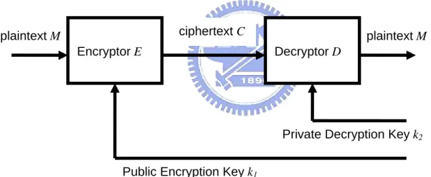
In general, a cryptosystem will have three roles during messages exchanging. They are sender, receiver and intruder. Typical cryptosystems are shown as Fig.2-1. At the sender side, sender encrypts plaintext M with an encryptor E and a key k1. The ciphertext is C = E
(M, k1). Then, the sender sends the ciphertext to public channel for receiver. When receiver
receives the ciphertext, he uses a decryptor D and key a k2 to decrypt ciphertext to plaintext.
channel and uses any kind of methods to know the plaintext from sender or pretend message to receiver. He can get ciphertext, but has no idea about k2.[4]
Fig. 2-1 Typical cripto-algorithm block diagram [4]
2.2 Symmetric and Asymmetric Cryptosystems
In typical cryptosystem, if secret k1 and k2 are the same, this cryptosystems are
Symmetric Key Cryptosystem, One-key Cryptosystem or Private Key Cryptosystem. Symmetric Key cryptosystems have been used for thousands of years. They range from simple substitution ciphers to more complex constructions. One of the simplest form is known as the Caesar cipher used by Julius Caesar. The process of Caesar cipher is simply shifting the alphabet [6]. This system is very easy to break. Fortunately, the growth of computing power and some new developments in mathematics make that it is possible to create Symmetric Key Cryptosystems that are unbreakable. Symmetric Key Cryptosystems are generally very fast. But they have a disadvantage. Sender and receiver need to agree on the shared key previously. However, the communicating parties may never meet over the network. It is impossible for the two parties to encrypt data without having a shared secret key that is known in advance. So, the Symmetric Key Cryptosystems are vulnerable.
The secret key sharing can be a major vulnerability in Symmetric Key Public Channel Decryptor D Encryptor E ciphertext C Intruder Sender Receiver k2 k1 plaintext M plaintext M
Cryptosystems. In 1976, Diffie and Hellman[7] demonstrated an algorithm which is known as Diffie-Hellman Key Exchange. It is an elegant approach toward secure communication that has led to the development of Public Key Cryptosystem, also named Asymmetric Cryptosystem. The use of Public Key Cryptosystem is quite simple. As shown in Fig.2-2., sender and receiver share a single public key, but receiver has one more key, private key. The public key is available to everyone in the world including the intruder, but the private key is only known by receiver. If sender wants to send message to receiver, sender uses the public key to encrypt message and then send to receiver. When receiver receives the ciphertext, he uses his private key to decrypt message. As a result, sender and receiver don’t have to exchange key previously. So, the Asymmetric Cryptosystems don’t have the vulnerability of symmetric cryptosystems.
Fig. 2-2 Public Key Cryptosystem
Symmetric cryptosystems are faster than asymmetric ones. They are the preferred mechanism for encrypting large amount of message. A cipher such as DES[8] will be at least 100 times faster than the asymmetric cipher RSA[9] in software and might be up to 10,000 times faster when implemented on specialist hardware.[6] Asymmetric cryptosystems are most suitable for protecting data with high security requirement. In practice, the most satisfactory methods are combining both symmetric and asymmetric systems. Use asymmetric systems to exchange secret key which is used by symmetric ones.
Public Encryption Key k1
plaintext M
Encryptor E Decryptor D
ciphertext C
Private Decryption Key k2
After secret key exchanging, the symmetric cryptosystems can encrypt or decrypt data with this key. DES and AES are the commonly used symmetric algorithms, and RSA is asymmetric one. In our research, we will focus on the three cryptographic algorithms.
2.3 AES[11]
In October 2000, the NIST chose Rijndael as the new Advanced Encryption Standard (AES). AES is intended to replace DES and Triple DES as a new secure standard [10].
AES is a symmetric block cipher. It can process block data of 128-bit. The Fig.2-3 shows the AES encryption flow. Just like all symmetric cryptographic algorithms. The AES has a regular computation flow. It just repeats the routine, round, some times depending on different length of cipher key. The length of cipher key are 128-, 192- and 256-bit respectively. The AES encryption and decryption are composed by five main components. All of them are Key Expansion, Subbytes, ShfitRows, Mixcolumn, and AddRoundKey. [11]
Fig. 2-3 Flow of AES
RoundKey1
RoundKeyNr AddRoundKey
Round 0 Key Expansion
FLOW AddRoundKey Round 1 128 RoundKey2 128 128 128 128 128 128 128 128 128 RoundKey0 Mixcolumn SubBytes ShiftRows plaintext(128 bits) ciphertext (128 bits) Round n SubBytes ShiftRows AddRoundKey
2.3.1 Definition
Before introducing AES, we must define some terms previously. The length of input, output, and state which is output of round in AES is 128 bits. This is represented by Nb = 4, which means the number of 32-bit words. The length of the cipher key, k is 128-, 192-, or 256-bit. The length of key is represented by Nk. The 128, 192, and 256 are Nk = 4, 6, and 8 respectively. Depending on different length of cipher key, AES algorithm performs some times of round. The round number is represented by Nr. When Nk is 4, 6, and 8, it means 10, 12 and 14 rounds in AES respectively. The combinations of Key-Block-Round are given as follow in Table. 2-1
Cipher Key length(Nk) Block Size(Nb) Number of Rounds(Nr)
AES-128 4 4 10
AES-192 6 4 12
AES-256 8 4 14
Table 2-1 Key-Block-Round Combination
2.3.2 Key Expansion
The Key Expansion algorithm takes cipher key to produces a key schedule for en/decryption flow. The Key Expansion will generate total Nb(Nr + 1) words. The Key Expansion processes shows as the following algorithm.
The SubBytes() is a function that perform four bytes table look up which will mention in section 2.3.3. The function RotWord() take a word [A1,A2,A3,A4] to perform a cyclic rotate, and then return the result [A2,A3,A4,A1]. And the Rcon[i] are constant in the form [Xi,0,0,0]. Xi are list as following table 2-2.
Round i 0 1 2 3 4 5 6 7 8 9
Xi 01 02 04 08 10 20 40 80 1b 36
KeyExpansion(byte key[4×Nk], word w[Nb×(Nr+1)], Nk) begin
word temp i = 0
while (i < Nk)
w[i] = word(key[4×i], key[4×i+1], key[4×i+2], key[4×i+3])
i = i+1 end while i = Nk while (i < Nb × (Nr+1)] temp = w[i-1] if (i mod Nk = 0)
temp = SubBytes(RotWord(temp)) xor Rcon[i/Nk] else if (Nk > 6 and i mod Nk = 4)
temp = SubWord(temp) end if
w[i] = w[i-Nk] xor temp i = i + 1
end while end
Take Nk = 4 as an example, the expansion executes as following Fig. 2-4
Fig. 2-4 Key Expansion Flow
2.3.3 SubBytes
Fig. 2-5 SubBytes applies S-box to each byte of the state
S-BOX Rotate &Table Rcon[0] Rcon[1]
…
⊕
⊕
⊕
⊕
Rotate &Table⊕
⊕
⊕
⊕
B
3,3B
3,2B
3,1B
3,0B
2,3B
2,2B
2,1B
2,0B
1,3B
1,2B
1,1B
1,0B
0,3B
0,2B
0,1B
0,0 Cipher keyB’
3,2B’
3,1B’
3,0B’
3,3B’
2,1B’
2,0B’
2,3B’
2,2B’
1,0B’
1,3B’
1,2B’
1,1B’
0,3B’
0,2B’
0,1B’
0,0The SubBytes transformation performs a non-linear byte substitution that operates independently on each byte as in Fig. 2-5. The non-linear byte substitution is constructed by the following transformation in Fig. 2-6. This transformation is invertible.
Fig. 2-6 SubBytes transformation
2.3.4 ShiftRows
Fig. 2-7 shift cyclically the state
In the ShiftRows transformation, the last three rows of the state rotate over different numbers of bytes like Fig.2-7. The shift numbers are listed in table 2-3.
No. of column C1 C2 C3
Left shift (Encryption) 1 2 3 Right shift (Decryption) 1 2 3
Table 2-3 Shift number C1 means Column one
1 0 0 0 1 1 1 1 1 1 0 0 0 1 1 1 1 1 1 0 0 0 1 1 1 1 1 1 0 0 0 1 1 1 1 1 1 0 0 0 0 1 1 1 1 1 0 0 0 0 1 1 1 1 1 0 0 0 0 1 1 1 1 1
=
b0 b1 b2 b3 b4 b5 b6 b7+
1 1 0 0 0 1 1 0 b0’ b1’ b2’ b3’ b4’ b5’ b6’ b7’B’
3,2B’
3,1B’
3,0B’
3,3B’
2,1B’
2,0B’
2,3B’
2,2B’
1,0B’
1,3B’
1,2B’
1,1B’
0,3B’
0,2B’
0,1B’
0,0B
3,3B
3,2B
3,1B
3,0B
2,3B
2,2B
2,1B
2,0B
1,3B
1,2B
1,1B
1,0B
0,3B
0,2B
0,1B
0,02.3.5 MixColumn
Fig. 2-8 Mixcolumn
The MixColumn operates column by column on the state. We can view it as a special matrix computation. It is shown as Fig.2-8. Before introducing the MixColumn, we must define some terms.
Definition
¾ Bi,C is byte : Bi,C ={b7,b6, b5, b4, b3, b2, b1, b0} ¾ B0,C ⊕ B1,C : B0,C XOR B1, C
¾ 01 ⊗ B0,C : {b7,b6, b5, b4, b3, b2, b1, b0}
¾ 02 ⊗ B0,C : {b6, b5, b4, b3⊕ b7, b2⊕ b7, b1, b0⊕ b7, b7}
¾ Hardware form of “02 ⊗ B0,C“ is shown as follows It is named X_TIME
Fig. 2-9 X_TIME Mix-Col
=
B0,c B1,c B2,c B3,c B’
0,c B’
1,c B’
2,c B’
3,c 02 03 01 01 01 02 03 01 01 01 02 03 03 02 01 01=
B0,c B1,c B2,c B3,c B’
0,c B’
1,c B’
2,c B’
3,c 0e 0b 0d 09 09 0e 0b 0d 0d 09 0e 0b 0b 0d 09 0e Encryption Decryption b’7 b’6 b’5 b’4 b’3 b’2 b’1 b’0 b7 b6 b5 b4 b3 b2 b1 b0⊕
⊕
⊕
B
3,3B
3,2B
3,1B
3,0B
2,3B
2,2B
2,1B
2,0B
1,3B
1,2B
1,1B
1,0B
0,3B
0,2B
0,1B
0,0B’
3,2B’
3,1B’
3,0B’
3,3B’
2,1B’
2,0B’
2,3B’
2,2B’
1,0B’
1,3B’
1,2B’
1,1B’
0,3B’
0,2B’
0,1B’
0,0Use the previous define, the encryption matrix can be expanded as follows.
B’0,C = 02 ⊗ B0,c ⊕ 03 ⊗ B1,c ⊕ 01 ⊗ B2,c⊕ 01 ⊗ B3,c
= 02 ⊗ B0,c ⊕ 02 ⊗ B1,c ⊕ 01 ⊗ B1,c ⊕ 01 ⊗ B2,c ⊕ 01 ⊗ B3,c The decryption shows as follows.
B’0,C = 0e ⊗ B0,c ⊕ 0b ⊗ B1,c ⊕ 0d ⊗ B2,c ⊕ 09 ⊗ B3,c
= 02 ⊗ B0,c ⊕ 02 ⊗ (02 ⊗ B0,c) ⊕ 02 ⊗ (02 ⊗ (02 ⊗ B0,c)) ⊕
01 ⊗ B1,c ⊕ 02 ⊗ B1,c ⊕ 02 ⊗ (02 ⊗ (02 ⊗ B1,c)) ⊕
01 ⊗ B2,c ⊕ 02 ⊗ (02 ⊗ B2,c) ⊕ 02 ⊗ (02 ⊗ (02 ⊗ B2,c)) ⊕
01 ⊗ B3,c ⊕ 02 ⊗ (02 ⊗ (02 ⊗ B3,c))
The Data flow graph of the two functions is shown as follows.
2.3.6 Add Round Key
Fig. 2-11 Add Round Key
In this transformation, it adds state and key scheduling like Fig.2-11
2.4 DES[8]
Data Encryption Standard (DES) derives from work done by IBM. It became effective in July 1977 and reaffirmed in 1983, 1988 and 1999. It is probably the most widely used secret key cryptosystem, particularly in securing financial data, such as Automated Teller Machines (ATMs).
Fig. 2-12 Flow of DES
64-bit plaintext Initial permutation Round 0 Round 15 Round 1 Inverse permutation 64-bit ciphertext
KEY CHEDULING
FLOW
Permuted choice248
Permuted choice248
Permuted choice248
Permuted choice1 56-bit key56
56
56
Left circular shift
Left circular shift
Left circular shift
ENCRYPTION
FLOW
B
3,3B
3,2B
3,1B
3,0B
2,3B
2,2B
2,1B
2,0B
1,3B
1,2B
1,1B
1,0B
0,3B
0,2B
0,1B
0,0B’
3,2B’
3,1B’
3,0B’
3,3B’
2,1B’
2,0B’
2,3B’
2,2B’
1,0B’
1,3B’
1,2B’
1,1B’
0,3B’
0,2B’
0,1B’
0,0 XOR keyThe DES flow is in Fig.2-12. It is composed by sixteen rounds and two permutations. The two permutations are place at beginning and end of DES round. In the key scheduling, DES needs only three kinds of permutations. As a result, we will divide DES in to two categories, Permutations and Round.
2.4.1 Permutations
In the Shift Left transformation, it treats input as two 28-bit blocks. Let’s note the 2 28-bit as C and D. The left rotating one bit means a rotation of the bits one place to the left. So after rotating one bit C and D become {C[0],C[28]…..C[1]}, {D[0],D[28]…..D[1]} separately. The rotate number depends on round iteration number. It shows as the following table.
Iteration 0 1 2 3 4 5 6 7 8 9 10 11 12 13 14 15 rotate bits 1 1 2 2 2 2 2 2 1 2 2 2 2 2 2 1
Table 2-4 Left shifts number
The Initial permutation, IP encipher the input block to the following permutation
58 50 42 34 26 18 10 2 60 52 44 36 28 20 12 4 62 54 46 38 30 22 14 6 64 56 48 40 32 24 16 8 57 49 41 33 25 17 9 1 59 51 43 35 27 19 11 3 61 53 45 37 29 21 13 5 63 55 47 39 31 23 15 7
That is the permuted input has bit 58 of the input as its first bit, bit 50 as its second bit, and so on with bit 7 as its last bit. The inverse permutation, IP-1, is list as following by the
40 8 48 16 56 24 64 32 39 7 47 15 55 23 63 31 38 6 46 14 54 22 62 30 37 5 45 13 53 21 61 29 36 4 44 12 52 20 60 28 35 3 43 11 51 19 59 27 34 2 42 10 50 18 58 26 33 1 41 9 49 17 57 25
Key scheduling is performed by three permutations Permutation choice 1 (PC1), Permutation choice 2 (PC2) and some left circular shift. PC1 is determined as follows.
57 49 41 33 25 17 9 1 58 50 42 34 26 18 10 2 59 51 43 35 27 19 11 3 60 52 44 36 63 55 47 39 31 23 15 7 62 54 46 38 30 22 14 6 61 53 45 37 29 21 13 5 28 20 12 4 PC2 is determined as follows. 14 17 11 24 1 5 3 28 15 6 21 10 23 19 12 4 26 8 16 7 27 20 13 2 41 52 31 37 47 55 30 40 51 45 33 48 44 49 39 56 34 53 46 42 50 36 29 32
2.4.2 Round
DES is composed by sixteen rounds. The Round organization is shown as follows in Fig.2-13. We first divide the input 64-bit into Right part and Left part. The R part is the f input. We XOR the result of f with L part to be R part of the next round. And the current R part will be the L part of the next round.
The function f performs the following operation. First, f expands input from 32-bit to 48-bit, and then XOR with Key scheduling. Second, separate the 48-bit into eight 6-bit data and then the eight 6-bit will look up 8 different tables individually. Each table will output 4-bit data. Finally, the eight 4-bit data will perform the finial permutation. The f finishes.
Fig. 2-13 Organization of Round The function of E 32 1 2 3 4 5 4 5 6 7 8 9 8 9 10 11 12 13 12 13 14 15 16 17 16 17 18 19 20 21 20 21 22 23 24 25 24 25 26 27 28 29 28 29 30 31 32 1 32
…..
f
Expand Permutation Look-Up Table 32 32 48 48 32 32 64-bit 64-bit 32 32 E XOR 6 6 S1 4 4 P⊕
⊕
S8The function of P 16 7 20 21 29 12 28 17 1 15 23 26 5 18 31 10 2 8 24 14 32 27 3 9 19 13 30 6 22 11 4 25
2.5 RSA[9]
In 1976, Diffie and Hellman propose an algorithm which leads to development of today’s Public Key Cryptosystems. After one year, three researchers at MIT used the suggestion of Diffie and Hellman to develop a method. The Three MIT researchers are Ron Rivest, Adi Shamir, and Leonard Adleman. The method is named after its founders, RSA. The RSA algorithm has become almost synonymous with Public Key Cryptosystems.
2.5.1 RSA Components[12]
For RSA, there are two components of RSA. z Choice of public key and private key z The encryption and decryption algorithm
RSA has two keys, public key for encryption, and private key for decryption. In order to choose public key and private key, doing the following flow is necessary.
z Choose two large prime numbers, p and q z Compute n = pq and z = (p-1)(q-1)
z Choose a number, e, less than n, and e and z with no comMon factor z Find a number, d, such that ed – 1 is exactly divisible by z
z The public key of RSA is (n,e), and the private key of RSA is (n,d) After get the keys the RSA flow shows as following.
z Ciphertext = C, and Plaintext = P.
z Public key is (n,e) and Private key is (n,d). z Encryption : C = Pe
mod n.
z Decryption :P = Cd
mod n.
2.5.2 Complexity of RSA
Before explain the complexity of RSA, we define one term as a basic unit to estimate result.
y Define :
1-bit addition or subtraction as a unit computation
In RSA, n times of modular-multiplications are required. Suppose (n,e) both are n bits, the RSA compute at least n times modular-multiplication. And each modular-multiplication needs total n2 times unit computation because one multiplication and one division are required. As a result, RSA needs O(n3) of computation.
There are two ways to speed up the RSA. The two algorithms are not conflict with each other. They can cooperate to speed up the RSA. They are Fast Exponentiation Algorithm and Montgomery Algorithm.
2.5.3 Fast Exponentiation Algorithm
Fast Exponentiation Algorithm is a trick to reduce the number of modular-multiplication from e times to log e. As previously described, we need at least n times modular-multiplication. However, it is not necessary to compute at least n times
modular-multiplication. For example, if we want to compute 816 mod 13. We can first compute 82 mod 13 with one modular-multiplication. Then, 84mod 13 come from by one modular-multiplication of 82 mod 13 and so on. As a result, 816mod 13 needs only four times of modular-multiplication. We reduce the number of modular-multiplication form e to log e. This is the concept of Fast Exponentiation Algorithm. A real case lists as follows.
1113 mod 53
11 mod 53 = 11
112 = 121, 112 mod 53 = 121 – 2×53 = 15
114 = (112)2 , 114 mod 53 = 152 mod 53 = 225 mod 53 = 225 – 4×53 = 13 118 = (114)2 , 114 mod 53 = 132 mod 53 = 169 mod 53 = 169 – 3×53 = 10 Therefore 1113 mod 53 = 11 × 13 × 10 = 1430 mod 53 =
1430 – 26×53 = 52
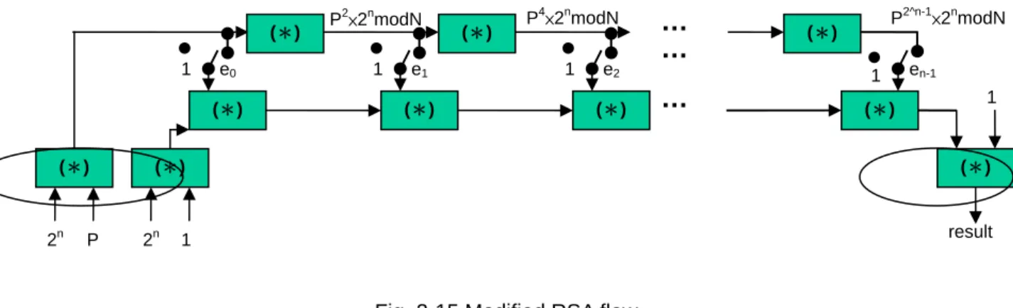
The Fast Exponentiation Algorithm applied to RSA is shown in Fig.2-14. The gray box is a modular-multiplication. P is plaintext. The bit notation of e in public key (n,e) is {ek ,…., e2,e1,e0}.
Fig. 2-14 Flow of RSA The Fast Exponentiation Algorithm shows as follows.
Fast-Ex (P,E,N) E, N < 2r. E = {e0, e1, e2, e3, e4, ….. en}, ei belong {1,0}. { var t0 = 1; 1 1 P (*) e0 e1 (*) P2modn P4modn e2 (*)
…
ei (*) (*) (*) (*) (*) en…
…
(*) P2^n-2modnvar t1 = P; for i=0 to n-1 begin if( ei = 1) then t0 = t0 × t1 mod N end if t1 = t1 × t1 mod N end for return t0; }
2.5.4 Montgomery Algorithm[13]
Fast Exponentiation Algorithm can reduce the modular-multiplication times in RSA. But computing a modular-multiplication still needs a lot of computation. In 1983, L.P. Montgomery proposed an algorithm that can speed up modular-multiplication.
For Fix N > 1, select a radix R coprime to N and the computation of modulo R are inexpensive to process. Let R-1 and N’ be integers satisfying 0< R-1 < N, 0 < N’ < R and R R-1 -NN’ = 1. For the given number, we can quickly compute the T R-1 mod N from T if 0< T < RN by the following algorithm REDC.
REDC(T)
m = (T mod R) N’ mod R
t = (T + mN)/R
if(t > N)then return t-N else return t
The result of REDC(T) will have the following characteristic. First, mN ≡ TNN’ ≡ -T mod R, so t is an integer. Second, tR ≡ T mod N so t ≡ T R-1 mod N. Third, 0< T+ mN < RN+RN, so 0 < t < 2N If we choose R = 2, the REDC will modify as follows.
REDC(T) (Radix 2)
N’ = N’n……N’2N’1N’0 N’i∈{1,0}
m =T0×N’0 mod 2
t = (T + mN) /R
if(t > N)then return t-N else return t
The -N’N mod 2 is equal to 1 and N0 is equal to 1 because N is the product of two large primes. As a result, N’ mod 2 is equal to 1. This will lead m equal to T0. We combine the multiplication and REDC(T) will get the Montgomery Algorithm shows as follow.
Mon ( A, B, N) (radix 2) A , B , N < 2r . A = {Ar,… A2 , A1,A0} Ai∋ {1,0} B = {Br ,… B2 ,B1 B0} Bi∋ {1,0} { var ACC = 0; for i=0 to r do
ACC = Ai×B+(AiB0^ACC0)×N >>1
end for return ACC; }
The result of Montgomery Algorithm is A×B×(2n)-1mod N. And the Montgomery Algorithm needs only n2 times of unit computation.
How does the Montgomery Algorithm reduce the computation? The Mon function has is a characteristic. If we process A to A×2n as A by doing Mon(A, 2nmodN, N), the result of Mon(A,A,N) will be A2×2n mod N, as A2. The preprocess can be done by Mon(A,22r,N). With the same way, we can get A4, A8 …A 2^i, … A2^n which needs only one Mon. (A2^i is A 2^i×2n mod N) To get the A2^imod N we need the post processing, Mon(A2^i,1, N). We call the preprocessing as mapping, and the post processing as remapping. This characteristic makes the number unit computations in
modular-multiplication from 2n2 to n2.
Fig. 2-15 Modified RSA flow
The flow applies Fast Exponentiation Algorithm and Montgomery Algorithm shows as Fig.2-15. The green box is a Montgomery Algorithm. The green box in circle in the left side is mapping. The right side is remapping. The algorithm of new RSA flow is following. RSA(M, E, N) E = { er, … e3, e4, e2 , e1, e0}, ei∋ {1,0}. { t=22r mod N; P = Mon( t, M, N); (Mapping) R = Mon( t ,1, N); (Mapping) for i=0 to r-1 do if( ei = 1) then R = Mon( R, P, N); end if P = Mon( P, P, N); end for R = Mon(1, R, N); (Re-mapping) return R; }
2.6 Some Hardware Implementations
There are many researches about cryptographic hardware design. We classify them
e0 P2×2n modN P 2n 1 1 … … 1 result (*) (*) (*) (*) (*) 1 e1 1 e2 … (*) (*) (*) (*) (*) 2n 1 en-1 P4×2n modN P2^n-1×2n modN
into two categories, Integrated Design and Dedicated Design. The Integrated design is able to perform more than two cryptographic algorithms. The dedicated design is dedicated to only one cryptographic algorithm.
2.6.1 Integrated Design
The Cryptonite processor is designed to provide a better tradeoff between flexibility and performance/area/power in the embedded systems, especially networking systems. It is a programmable architecture dedicated to cryptographic applications namely DES/3DES, AES, RC6, IDEA, MD4, MD5, SHA-1.
Fig. 2-16 Cryptonite Architecture
Architecture of Cryptonite shows as Fig. 2-16. It is two independent computing clusters, one for encryption and another for on-the-fly key generation. In general, key generation is independent to en/decryption flows. Coarse-grain parallelism can be exploited. On-the-fly key generation is vital for embedded systems solutions because storing/retrieving the round key needs for hundreds or thousands of cycle is not feasible. As
a result, Cryptonite provides two independent computing clusters. There are four components, Control Unit, ALU, Address Generation Unit and Data I/O Unit in one computing cluster.
The Control Unit puts all other units on hold and grants the External Access Unit access to the internal data paths. Besides control other unit, Control Unit also provides 16 register for loop and control branch.
Fig. 2-17 ALU of Cryptonite
The ALU of Cryptonite shows as Fig. 2-17. There three main part of Cryptonite, register file, Arithmetic Unit and XOR unit. The register file is consisted of four 64-bit register. In order to compensate for the low register count, each register can be either used as one 64-bit or 2 32-bit registers. The AU supports conventional arithmetic operations, boolean operations and specialized functions supporting certain algorithms. The XU can provide six operand XOR.
Address Generation Unit contains small add/sub/and ALU for address generation. It supports eight addressing modes. The Data I/O Unit contains two data buffer for input/output. Data I/O Unit also contains a specialized DES unit. Fast DES execution not only needs highly specialized operations but also S-Box access to memory. Hence the DES is dedicated in the Data I/O Unit rather than ALU.
We compare our proposed design with Cryptonite in the following table.
Cryptonite Proposed design
Hardware organization ASIP Reconfigure Hardware
Parallelism Coarse grain Fine grain
Key gen. On the fly Generate previously
AES
Implementation Integrate to other algorithm Integrate to other algorithm
Key gen On the fly On the fly
DES
Implementation Dedicated module Dedicated module
Support DES/3DES, AES, RC6, IDEA,
MD4, MD5, SHA-1
DES/3DES, AES,RSA
Environments High-end system Low-end system
Flexibility Cryptonite > Proposed design
Area Cryptonite > Proposed design
Speed Cryptonite < Proposed design
Table 2-5 Comparison of Cryptonite and proposed design
Besides the cryptonite other industrial implementation will list in Appendix A-2
2.6.2 Dedicated Design
AES
[15] proposed a special purpose ASIC processor that implements the AES. In its implementation, there is only one hardware for en/decryption round and re-use the same piece to complete the whole en/decryption. Besides hardware reusing, the processor is also designed to complete one encryption round in one clock cycle. Furthermore, it uses on-the-fly key generation for encryption and generating the all key beforehand for
decryption. For SubBytes, it uses ROM to implement the SubBytes.
Its architecture is shown as Fig. 2-18. There are two main modules for AES. One for encrypt another for Key Expansion. Besides the two processing components, there are three interfaces. The Processor FSM is top-level controller interfacing with the user module. The input and output FSM is used to control input and output channel.
Fig. 2-18 Organization of [15]
Besides the research about the architecture of AES, there are some researches which focu on SubBytes. In [16], they propose a compact S-Box based on composite field. Using the composition field ,we can get smaller area of S-box.
H.Kuo A. Satoh
Unroll loop No No
SubByte ROM Dedicated Design
Area H.Kuo > A. Satoh
Speed H.Kuo < A. Satoh
DES
In [17], this paper presents two FPGA implementations of DES. Both permit different pipeline levels with 21 and 37 cycles. As the section 2.4 shows, DES has some combinations and permutations operation. They are IP, IIP, E, and P in the Fig. 2-18. The S means S-box. The ⊕ means XOR. R means E-1 which is an inverse operation of E. The two new pipeline of DES are shows as follows. In the Fig 2-18, the left side is DES core one with 21 pipe stages, another is core two with 37 pipe stages. [17] wants to reduce the critical path and provide higher throughput by reorder the E in the DES flow.
Fig. 2-19 The new DES pipeline
Rouvroy -1 Rouvroy -2
Unroll loop Yes Yes
Pipe stages 37 21
Area Rouvroy -1 > Rouvroy -2
Speed Rouvroy -1 > Rouvroy -2
RSA
The Montgomery Algorithm has a modified version. Unlike the original one, Mon(A,B,N) A,B,N < 2n, which adds N along with partial product of A×B, the modified one adds N after finishing A×B. In Modified Montgomery algorithm, it splits modular-multiplication operation into multiplication procedure and Montgomery modular reduction procedure. Modular reduction procedure adds N 2n times to the accumulated result which is produced from the multiplication procedure.
In [18], they also based on the enhanced Modified-Montgomery Algorithm. Unlike previous implementation, they use one linear Bit-level Cellular-Array Design to perform the two procedures. The linear Bit-level Cellular-Array is Baugh-Wooley 2’s complement array multiplier.
In [19], it based on original Montgomery Algorithm. Its architecture shows as follows. It is consisted of a linear Processing element (PE). Each PE performs fix length addition. Use these PEs to perform the all addition of RSA. The all architecture is like serial parallel multiplier.
Fig. 2-20 Organization of [19]
Blum & Paar Su & Hwang
Mon Original Modified
Organization Serial-parallel multiplier Baugh-Wooley multiplier
Area Medium Large
Speed Medium High
Chapter 3 Design
In this chapter, we first summarize the all operation of the three cryptographic algorithms by its characteristic and classify them into three categories. Then design the components for the categories respectively.
3.1 Function Requirement
Cipher Function Comment
XOR 8 bits xor
Table look up 8 bits in/8 bits output.
Key expansion
Rotate Byte Rotate left 1 bytes
X_TIME Special operation for Galois field
XOR 8 bits xor
Table look up 8 bits in/8 bits output.
AES
Round
Rotate Byte Rotate right or left 1, 2, and 3 bytes
PC-1 Permutation bits from 64 bits to 56 bits
PC-2 Permutation bits from 56 bits to 48 bits
Key scheduling
Shift 1 or 2 Shift left and right 28 bits one or two bits individually
Expand E Expand input form 32 bits to 48 bits
Permutation P Permutation 32 bits
XOR 48 and 32 bits XOR
DES
Round
Table look up 6 bits in 4 bits out
Addition
RSA MON
Shift Shift right one bits
Table 3-1 Function requirements
At Chapter 2, we introduce for the three cryptographic algorithms. At this Chapter we first summarize the function requirement of the three algorithms in Table 3-1. In table 3-1, the function requirements for the three cryptographic algorithms are listed. These function requirements can be classified into three kinds depending on their characteristic. In Table 3-2, shows the three categories.
Class Type Algorithm Comment
Expand DES 32 bits to 48 bits
Permutation function DES 32 bits permutation
Initial permutation DES Start of the flow 64 bits to 64 bits
Inverse permutation DES End of the flow 64 bits to 64 bits
Rotate Bit DES Rotate left one or two bits
Permutation Choice 1 DES 64 bits to 56 bits
Permutation Choice 2 DES 56 bits to 48 bits
Rotate Byte AES byte level rotate left or right
Permutation & Combination
Shift MON Shift one bit
XOR DES,AES 8 or 32 bits xor
Xtime AES special operation for Galois field
Computation
Addition MON
Buffer DES,AES,MON Memory output buffer
Memory
Look-up table DES,AES Table look up
Table 3-2 Operation classification
These three categories are Permutation & Combination, Computation and Memory. Permutation & Combination are some fix wiring operation of the three cryptographic algorithms. Computation is the operators which are belong to arithmetic and logic. The three cryptographic algorithms need only Addition, XOR and X_TIME. The finial class is Memory which is table look up and data buffer in the three cryptographic algorithms. Because of the three classes, our system will have the three components to perform the three kinds of operation respectively.
Before design module for the three class operation, we notice that DES has some characteristics. First, DES is suit for on-the-fly key generation. So, the hardware cost for
DES key generation is small. Second, the hardware circuit for table look up in DES is small too. Because these two reasons, we dedicated part of DES for get better result.
3.2 System Overview
As the section 3.1 described, our system overview is shown in Fig. 3-1. We have six components. They are Permutation & Combination Unit, Computation Unit, Memory Unit, DES Unit, Context Memory/Decoder and Ctrl.
Fig. 3-1 System overview
Permutation & Combination Unit (PCU-1 or PCU-2) :
The Permutation & Combination Unit (PCU) executes the fix wiring tasks. As cryptographic algorithms go, PCU routes the data to Computation Unit or Memory Unit. In DES, there are many wiring operation, such like PC1, PC2, Expand and etc. The most operation wiring of DES is in this unit.
P.E.
…..
MUXPCU-1 CU
MU
Context decoder P.E input buffer Context memoryCtrl
CMD
128input
Output
P.E. P.E. P.E. 128DES
PCU-2
Computation Unit (CU) :
The Computation Unit performs arithmetic or logic operators of three cryptographic algorithms. It is composed by processing elements (PE) and some additional circuits for MON. Each PE is a functional unit which has its own register file which stores immediate data during execution. The additional circuits will introduce at section 3.4.4.
DES UNIT
This unit performs some DES operation to get better space-time product. It supports on-the-fly key generation.
Memory Unit (MU) :
As the Montgomery Algorithm goes, it needs to store large immediate data and preload data for smooth execution. Besides the Montgomery Algorithm, DES and AES also need to look up table. As a result, Memory Unit is used to store immediate data and preload buffer of MON and look-up table for DES and AES
Context Memory/Decoder (CMD) :
The three cryptographic algorithms needs different context to control CU, PCU, and MU. We use the Context Memory (CM) to store the context for each cryptographic algorithm. Context Decoder (CD) decodes the context to control signals.
Control Unit (Ctrl) :
Ctrl is the central control unit to control the whole hardware. It consists of a finite state machine, some flow registers, address register and address generation function. It uses the finite state machine to control our hardware and the flow registers to control the flow of the three cryptographic algorithms.
3.3 Permutation and Combination Unit
Permutation and Combination Unit is used to route data between CU and MU. In the following table, it shows the permutations and combinations perform by this unit.
If we use high flexibility implementation, such as GRP [20],OMFLIP[21], CROSS [22], and BFLY [23][24]. These will lead to high area cost. As a result, we just make our PCU to perform the fix permutation or combination wiring. It operation is shown in the Table 3-3
Unit Type Algorithm Comment
Initial permutation DES Start of the flow 64 bits to 64 bits
Permutation Choice 1 DES 64 bits to 56 bits
PCU-1
Rotate Byte AES byte level rotate left or right
PCU-2 Inverse permutation DES End of the flow 64 bits to 64 bits
Table 3-3 Permutation and combination performed by PCU
3.4 Computation Unit
The CU performs tasks of logic operators of three cryptographic algorithms. The CU is composed by processing elements (PE). Each PE has its own register file to store immediate data. For Montgomery Algorithm consideration, CU needs additional circuits to execute Montgomery Algorithm. First we will introduce the PE design and then introduce these additional circuits in section 3.4.4.
3.4.1 Observation
Before design our PE, we first introduce the tasks of PE and some observations. For full parallelism, The hardware resource needed by AES and MON is shown in Table 3-4.
AES_D (128) AES_E(128) Mon(1024)
XOR(8 bits) 9×16×10+32 9×16×5+32 >1024×128×2
X_TIME(8 bits) 9×16×6 9×16×1 0
As the section 2.3.5 and 2.3.6 described, the data flow graph of AES which combines the MixColumn and the AddRoundKey is shown in Fig.3-2. The AES-128 composed by 9 rounds and two additional AddRoundKey. As a result, the XOR requirements of en/decryption are 9×16×5+32 and 9×16×10+32 and X_TIME are 9×16×6 and 9×16×1separately.
An addition is composed by two XOR. In Mon (1024), we know that it works like a multiplier. The original Montgomery Algorithm needs total 1024 times of 1024-bit addition. Now, we formalize 1024-bit addition to 128 times 8 bits addition. This is why the Mon needs at least 1024*128*2 time 8 bits addition.
As a result, the MON needs only Double XOR. It shows as in Fig. 3-3.
Fig. 3-2 En/Decryption data flow graph of Mixcolume and AddroundKey
So the computation granularities between the three cryptographic algorithms are shown in Fig. 3-4. AES has coarser granularity. MON have finer granularity.
Fig. 3-4 Granularity of the two cryptographic algorithms
3.4.2 Organization of Computation Unit
As the observation of 3.4.1 described, the MON needs only simple hardware for execution. So, the Mon will interleave store and addition. As a result, too much complicated hardware will be useless. Our CU organization is shown in Fig. 3-5. It is a one dimension array of PE. The direction of data inputs stream is vertical to the one dimension array. Each PE has the ability to perform the three algorithms. The more PE have, the higher parallelism we have.
Fig. 3-5 Organization of CU
If we want to design an organization of PE which gets better space-time product, we must make hardware idle as less as possible. There are two kinds of design method to analysis data flow graph of the three algorithms.
z Partition AES to fit MON. z Put MON into AES.
In the first method, it is finding a smallest hardware which can be divided by AES en/decryption, MON, like LCM. The second method is like to find GCD. Because the first
P.E
P.E
P.E
P.E
P.E
P.E
AES_DE AES_EN
:
AES MON
method will produce smaller hardware unit, it will suit for embedded system to scale than hardware produced by second method. As a result, we choose the first methodology.
3.4.3 Design of P.E.
We have chosen the first method to analysis in order to get small space-time product. It seems no trivial solution. So, we have proposed a structural methodology to decide our PE organization. The concept our methodology is that
z Candidate Choosing : We choose some possible candidates of P.E. organization, then design it dedicatedly
z Evaluation : Evaluate the possible candidates
Candidate Choosing
Before introducing our methodology, we must define some terms previously. The organization of PE comes from OPSET.
Definition
z OP : A connected direct graph composed by XORS and/or X_TIMEs
z OP_LEN : Number of nodes in critical path of OP.
z OPSET i : A set of OPs that can consist the three data flow graph
The principle of our OPSET i finding is shown as following.
1. First OP
OP_LEN is i
Most frequent OP and occur more than twice
2. Other OPs
Dependent on occurrence frequency
OPSET 1 (I)
Fig. 3-6 Partition AES and MON The OP set is
Fig. 3-7 OP set for OPSET 1 The P.E. organization of OPSET 1 is in Fig. 3-8.
Fig. 3-8 OPSET 1 organization M U X X T SRC_B SRC_A Cin M U X X Carry_chain
OPSET 2 (II)
Fig. 3-9 Partition AES and MON The OP set is
Fig. 3-10 OP set for OPSE 2 The P.E. organization of OPSET 2 is in Fig. 3-11.
Fig. 3-11 OPSET 2 organization M U X X T X SRC_B SRC_A Cin SRC_C MU x Carry_chain
![Fig. 1-2 Throughput of high- and low- end embedded processors [2]](https://thumb-ap.123doks.com/thumbv2/9libinfo/8746617.205106/16.892.153.694.112.738/fig-throughput-high-low-end-embedded-processors.webp)

![Fig. 2-5 SubBytes applies S-box to each byte of the state S-BOX Rotate &Table Rcon[0] Rcon[1] …⊕⊕⊕⊕Rotate &Table ⊕⊕ ⊕ ⊕ B3,3 B3,2 B3,1 B3,0 B2,3 B2,2 B2,1 B2,0 B1,3 B1,2 B1,1 B1,0 B0,3 B0,2 B0,1 B0,0 Cipher key B’3,2B’3,1 B’3,0 B’3,3B’2,1B’2,0 B’2,](https://thumb-ap.123doks.com/thumbv2/9libinfo/8746617.205106/26.892.96.795.536.1040/subbytes-applies-state-rotate-table-rotate-table-cipher.webp)