236 IEEE PHOTONICS TECHNOLOGY LETTERS, VOL. 22, NO. 4, FEBRUARY 15, 2010
Temperature-Dependent Electroluminescence
Efficiency in Blue InGaN–GaN Light-Emitting
Diodes With Different Well Widths
C. H. Wang, J. R. Chen, C. H. Chiu, H. C. Kuo, Senior Member, IEEE, Y.-L. Li, T. C. Lu, Senior Member, IEEE,
and S. C. Wang, Life Member, IEEE
Abstract—Temperature dependence of electroluminescence
(EL) efficiency in blue InGaN–GaN multiple-quantum-well (MQW) light-emitting diodes (LEDs) with different well widths is systematically investigated. The EL efficiency at 300 K shows a maximum at the input current of 4, 10, and 60 mA for the LEDs with 1.5-, 2.0-, and 2.5-nm QWs, respectively. Nevertheless, the droop behavior at 80 K is mainly dominated by the low hole mobility and near independence on the QW thickness. According to the simulation results, it is found that the distinct efficiency droop behavior for the LEDs with different well widths at high and low temperature is strongly dependent on the effects of elec-tron overflow and nonuniform hole distribution within the MQW region.
Index Terms—Efficiency droop, electroluminescence (EL),
light-emitting diodes (LEDs), quantum wells (QWs).
I. INTRODUCTION
I
II–NITRIDE based light-emitting diodes (LEDs) have been developed in various applications due to their widely tunable wavelength from ultraviolet to blue/green [1]. Never-theless, the most expected application, solid-state lighting, is still developing, which means the state-of-the-art InGaN–GaN LEDs should be further improved. Although the light-extrac-tion efficiency has been significantly improved by different techniques [2], the internal quantum efficiency (IQE) still suffers a major obstacle, i.e., the substantial decrease in effi-ciency with increasing injection current [3], [4]. This effieffi-ciency droop behavior strongly limits the development of many spe-cific applications which require the operation current of the InGaN–GaN LEDs under high injection levels. Several possible physical mechanisms leading to efficiency droop have been proposed, including carrier leakage from the active region [5]–[7], carrier delocalization [8], and Auger recombination Manuscript received September 29, 2009; revised November 14, 2009; accepted November 24, 2009. First published January 12, 2010; current version published January 27, 2010. This work was supported in part by the National Science Council in Taiwan under Grant NSC96-2221-E-009-095-MY3 and Grant NSC96-2628-E-009-017-MY3.C. H. Wang, J. R. Chen, C. H. Chiu, H. C. Kuo, T. C. Lu, and S. C. Wang are with the Department of Photonics and Institute of Electro-Optical Engi-neering, National Chiao Tung University, Hsinchu 30050, Taiwan (e-mail: hckuo@faculty.nctu.edu.tw).
Y.-L. Li is with the Institute of Photonics and Optoelectronics, National Taiwan University, Taipei 10617, Taiwan (e-mail: yunli@cc.ee.ntu.edu.tw).
Color versions of one or more of the figures in this letter are available online at http://ieeexplore.ieee.org.
Digital Object Identifier 10.1109/LPT.2009.2037827
[9]. However, the major mechanism resulting in the efficiency droop has not been established. In this study, we systematically investigated the temperature-dependent electroluminescence (EL) efficiency in blue InGaN LEDs with different well widths. The injection current achieving the maximum EL efficiency is closely dependent on the well widths and temperatures. Additionally, the temperature dependence of current versus forward-voltage ( – ) characteristics is investigated to estab-lish the relationship between forward voltage and EL efficiency under different temperatures.
II. EXPERIMENTS
The InGaN–GaN LEDs were grown on -plane sapphire sub-strates by metal–organic chemical vapor deposition (MOCVD). On top of the sapphire substrate, a 20-nm-thick GaN nucleation layer was grown at low temperature followed by a 4- m n-type GaN buffer layer. After the growth of the buffer layer, a ten-pe-riod InGaN–GaN multiple-quantum-well (MQW) was grown. A 10-nm p-type AlInGaN layer was grown on top of the MQWs and followed by two sets of p-type AlGaN–GaN (10 nm/2 nm) electron blocking layers (EBLs). Finally, a heavily Mg-doped p-type GaN contact layer ( 120 nm) was grown. Subsequently, the LED mesa with an area of the 350 350 m was defined by using standard photolithography and dry etching. In addition, a transparent conduction indium tin oxide layer was employed to be the p-type Ohmic contact layer. Ni–Au and Ti–Al–Ti–Au metallizations are deposited by e-beam evaporation to serve as p-type and n-type Ohmic contacts, respectively. The QW thick-nesses of the InGaN LEDs were controlled by changing the growth time of 1 min (1.5 nm), 1.33 min (2.0 nm), and 1.67 min (2.5 nm). The LED chips were mounted onto TO-46 lead-frames without epoxy encapsulation.
III. RESULTS ANDDISCUSSION
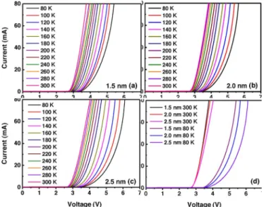
Fig. 1 shows the measured – characteristics of the InGaN LEDs with different well widths of (a) 1.5, (b) 2.0, and (c) 2.5 nm under different temperatures. The forward voltage of the InGaN LEDs increases with decreasing temperature, which mainly originates from the reduction of hole mobility and the difficulty in activating hole concentration due to the high activation energy of Mg dopants. For clearly comparing the – curves of the LEDs with different well widths at high and low temperatures, we further summarized the results at 80 K and 300 K, respectively, in Fig. 1(d). It is noteworthy that the necessary forward voltage significantly increases from 300 K to 1041-1135/$26.00 © 2010 IEEE
WANG et al.: TEMPERATURE-DEPENDENT EL EFFICIENCY IN BLUE InGaN–GaN LEDs 237
Fig. 1. MeasuredI–V characteristics of the InGaN LEDs with different well widths of (a) 1.5, (b), 2.0, and (c) 2.5 nm under different temperature. TheI–V curves at high and low temperature are further summarized in (d).
80 K by nearly 1.5–2.0 V with increasing QW thickness when the injection current is 80 mA. Previously, Cao and LeBoeuf demonstrated that when the temperature decreases from room temperature (300 K) to low temperature (80 K), the electron concentration and mobility of n-type GaN would be decreased by several times. However, the hole concentration and mobility of p-type GaN would be decreased by two orders and by about one order, respectively [10]. This dramatically reduced hole concentration and mobility at low temperature will result in significantly nonuniform carrier distribution within the ten-pair MQW active region. Therefore, we deduced that the increased forward voltage with well width is resulted from the increased undoped region and the difficulty of hole transport between each QW at low temperature.
To investigate the carrier transport within MQW region, sim-ulations of the band diagrams and carrier distributions were per-formed by employing the APSYS modeling software. Fig. 2 shows the calculated band diagrams under an injection current of 80 mA for the LEDs with 1.5- and 2.5-nm wells at 80 K and 300 K. Since the LED with thicker well (2.5 nm) requires higher forward voltage than that with thinner well (1.5 nm) under the same injection current at 80 K, the conduction band on the n-side of the LED is higher than that on the p-side, which favors the electrons to escape to the p-side of the LEDs from the observa-tion of electron quasi-Fermi level in the EBL region, as shown in Fig. 2(b). On the contrary, when the temperature increases to 300 K, the thermally activated hole concentration and thermally enhanced hole transport lead to the relatively minor difference in forward voltage between the LEDs with 1.5- and 2.5-nm wells, resulting in the relatively flat conduction band on the n-side and p-side, as shown in Fig. 2(c) and (d). Fig. 3 shows the calcu-lated hole concentration distributions under the injection cur-rent of 80 mA at 80 K and 300 K for the LED with 2.5-nm well width. As can be seen from Fig. 3, the hole concentration in the QW nearest the p-side is about two orders of magnitude higher than that in the QW nearest the n-side when the temper-ature is 80 K. This nonuniform hole distribution will strongly
Fig. 2. Calculated band diagrams under an injection current of 80 mA for the LEDs with 1.5- and 2.5-nm wells at 80 K and 300 K.
Fig. 3. Calculated hole concentration distributions under the injection current of 80 mA at 80 K and 300 K for the LED with 2.5-nm wells.
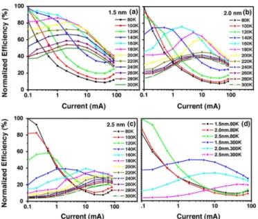
enhance the electron overflow from the QWs as well. When the temperature is increased to 300 K, the relatively uniform hole distribution within the MQW region can effectively enhance the radiative recombination in each QW. Consequently, the energy band diagram is strongly influenced by temperature-dependent forward voltage, which will play an important role in the temper-ature dependence of EL efficiency as a function of input current. Fig. 4 shows the measured results of external quantum efficiency (EQE) versus logarithmic input current at temper-ature between 80 K and 300 K for the LEDs with different well widths. The maximum EQE is normalized in Fig. 4. It can be found that the maximum EL efficiency shifts toward lower injection current with decreasing temperature. When the temperature is 80 K, the rapid efficiency droop is induced from the severely nonuniform hole distribution, as shown in Fig. 3. Under the condition of low temperature and low current injection ( 0.1 mA), holes are confined in the QW nearest the p-side, which results in the effective recombination in this QW due to the relatively easy electron transport through the MQW region. Nevertheless, with increased injection current, holes are still confined in this QW due to the low mobility
238 IEEE PHOTONICS TECHNOLOGY LETTERS, VOL. 22, NO. 4, FEBRUARY 15, 2010
Fig. 4. Measured normalized EQE of the blue InGaN LEDs with different well widths as a function of input current at temperature between 80 K and 300 K.
at low temperature and electrons seriously overflow into the p-side since the increase of injection current requires large for-ward voltage at low temperature, leading to the corresponding change in energy band structure, as shown in Fig. 2(b). The significant nonuniform hole distribution and electron overflow cause the rapid EL efficiency droop with increasing input current at low temperature. Furthermore, in the case of high temperature (300 K), the EL efficiency raises at first and then decreases with the increasing injection current. This is quite different as compared with the case at low temperature. As we know, the efficiency would be increased with decreasing temperature because of the suppression of nonradiative recom-bination centers. However, from simulation results of Fig. 3, severer nonuniformity of hole distribution at MQWs at low temperature reduced the luminescence efficiency, especially at higher injection level. Suppression of nonradiative centers and poorer hole distribution phenomenon will compete with each other and, therefore, a maximum efficiency would be observed at each temperature.
To further study the temperature-dependent carrier transport in the LEDs with different well width, we summarized the EL efficiency at 80 K and 300 K in Fig. 4(d). It is obvious that the EL efficiency curves nearly follow the same droop behavior at low temperature for the three LED structures. The EL efficiency of the LEDs with different well widths have a minimum value at 80 K as the input current is about 40 mA. It means that the droop behavior is dominated by the low hole mobility and is in-dependent on the QW thickness. This phenomenon also implies that the efficiency droop is less sensitive to the Auger recombi-nation since the droop behavior is obviously observed at low in-jection current. The distinct EL efficiency as a function of input current is found at 300 K for the three LEDs. A much lower effi-ciency droop is observed for the LED with 2.5-nm QW with in-creasing injection current. However, the LED with thicker QW
gives rise to lower EL efficiency, as shown in Fig. 4(d). It is at-tributed to spatial separation of electrons and holes induced by the stronger internal polarization field. Furthermore, to achieve maximum EL efficiency, the required input current values are very different for the three LED structures. The input current values achieving maximum EL efficiency are around 4, 10, and 60 mA for the LEDs with 1.5-, 2.0-, and 2.5-nm QWs, respec-tively. The efficiency droop from the maximum value is dom-inated by the effect of electron overflow at 300 K. The LED with 2.5-nm QWs can effectively confine electrons within the MQWs and suppress the electron overflow as compared with the LED with thinner QWs, which causes that the maximum EL efficiency shifts toward higher injection current with the in-creased QW thickness.
IV. CONCLUSION
In summary, we have presented the temperature-dependent efficiency droop in blue InGaN LEDs with different well widths. At low temperature, the droop behavior is dominated by the low hole mobility and is nearly independent on the QW thickness. However, at high temperature, the input current values achieving maximum EL efficiency are around 4, 10, and 60 mA for the LEDs with 1.5-, 2.0-, and 2.5-nm QWs, respectively. This dif-ference of the efficiency droop at high and low temperature is closely relevant to the effects of carrier transport and escape pro-cesses from the active region and is less sensitive to the Auger recombination.
REFERENCES
[1] S. Nakamura and G. Fasol, The Blue Laser Diode. New York: Springer, 1997.
[2] H.-W. Huang, C. C. Kao, J. T. Chu, H. C. Kuo, S. C. Wang, and C. C. Yu, “Improvement of InGaN–GaN light-emitting diode performance with a nano-roughened p-GaN surface,” IEEE Photon. Technol. Lett., vol. 17, no. 5, pp. 983–985, May 2005.
[3] J. Xu, M. F. Schubert, A. N. Noemaun, D. Zhu, J. K. Kim, E. F. Schubert, M. H. Kim, H. J. Chung, S. Yoon, C. Sone, and Y. Park, “Reduction in efficiency droop, forward voltage, ideality factor, and wavelength shift in polarization-matched GaInN/GaInN multi-quantum-well light-emitting diodes,” Appl. Phys. Lett., vol. 94, p. 011113, 2009.
[4] Y.-L. Li, Y.-R. Huang, and Y.-H. Lai, “Efficiency droop behaviors of InGaN/GaN multiple-quantum-well light-emitting diodes with varying quantum well thickness,” Appl. Phys. Lett., vol. 91, p. 181113, 2007. [5] M.-H. Kim, M. F. Schubert, Q. Dai, J. K. Kim, E. F. Schubert, J. Piprek,
and Y. Park, “Origin of efficiency droop in GaN-based light-emitting diodes,” Appl. Phys. Lett., vol. 91, p. 183507, 2007.
[6] M. F. Schubert, J. Xu, J. K. Kim, E. F. Schubert, M. H. Kim, S. Yoon, S. M. Lee, C. Sone, T. Sakong, and Y. Park, “Polarization-matched GaInN/AlGaInN multi-quantum-well light-emitting diodes with reduced efficiency droop,” Appl. Phys. Lett., vol. 93, p. 041102, 2008. [7] Y.-K. Kuo, J.-Y. Chang, M.-C. Tsai, and S.-H. Yen, “Advantages of blue InGaN multiple-quantum well light-emitting diodes with InGaN barriers,” Appl. Phys. Lett., vol. 95, p. 011116, 2009.
[8] B. Monemar and B. E. Sernelius, “Defect related issues in the “current roll-off” in InGaN based light emitting diodes,” Appl. Phys. Lett., vol. 91, p. 181103, 2007.
[9] K. T. Delaney, P. Rinke, and C. G. Van De Walle, “Auger recombina-tion rates in nitrides fro first principles,” Appl. Phys. Lett., vol. 94, p. 191109, 2009.
[10] X. A. Cao and S. F. LeBoeuf, “Current and temperature dependent characteristics of deep-ultraviolet light-emitting diodes,” IEEE Trans. Electron Devices, vol. 54, no. 12, pp. 3414–3417, Dec. 2007.