國立高雄應用科技大學
電子工程研究所
碩士論文
利用克爾型非線性金屬絕緣體金屬表面電漿波導結構設計新
全光式非線性元件
New design of all-optical devices based on Kerr-type
nonlinear metal-insulator-metal surface plasmonic
waveguide structures
研 究 生:趙 冠 羽
指導教授:吳 曜 東
利用克爾型非線性金屬絕緣體金屬表面電漿波導結構設計新全光式非線
性元件
New design of all-optical devices based on Kerr-type nonlinear
metal-insulator-metal surface plasmonic waveguide structures
研 究 生: 趙 冠 羽 Student: GUAN-YU JHAN
指導教授: 吳 曜 東 Advisor: YAW-DONG WU
國立高雄應用科技大學
電子工程研究所
碩士論文
A Thesis
Submitted to
Institute of Electronics Engineering
National Kaohsiung University of Applied Sciences
in Partial Fulfillment of the Requirements
for the Degree of
Master of Engineering
in
Electronic Engineering
June 2015
Kaohsiung, Taiwan, Republic of China
中 華 民 國 一 百 零 四 年 六 月利用克爾型非線性金屬絕緣體金屬表面電漿波導結構設計新
全光式非線性元件
學生:趙冠羽 指導教授:吳曜東 博士
國立高雄應用科技大學
電子工程研究所
摘要
本論文探討表面電漿波導元件的特性,吾人對金屬絕緣體金屬電漿波導結構與加入 Kerr 型非線性材料的結構來做探討。非線性材料其特性為介質會隨著電場強度的變化而改 變折射率。 首先,吾人使用碟型波導共振的特性,將非線性材料填入共振腔中,透過調整碟型共 振腔的半徑大小和耦合孔徑的寬度,來濾出特定波長,再調整共振腔的耦合距離,來得到 帶阻的效果,再利用輸入電場強度的改變,來設計全光式邏輯閘,而高態傳輸效率達到 94%, 低態為 0.002%。接下來增加碟型共振腔的數量,利用所得到的帶阻寬度,來設計所有的全 光式邏輯閘。及閘(AND GATE) 在高態傳輸效率達到 94.5%而在低態時僅為 0.002%。或閘(OR GATE) 在高態傳輸效率達到 95.4%而在低態時僅為 0.002%。反或閘(NOR GATE) 在高
態時的傳輸效率達到 97.4%而在低態時僅為 0.003%。互斥反或閘(XNOR GATE) 在高態傳 輸效率達到 97.4%而在低態時僅為 0.004%。反及閘(NAND GATE) 在高態傳輸效率達到 97.3%而在低態時僅為 0.002%。互斥或閘(XOR GATE) 在高態傳輸效率達到 97.3%而在低態 時僅為 0.002%。 最後,吾人利用三角齒型共振腔的特性為基礎,透過選擇適當的長度與耦合距離濾出 特定波長,再藉由填入克爾型非線性材料,設計一新穎的全光式三工器的分波多工器(WDM),
此三工器可以分別濾出 1310nm、1490nm、1550nm 光通訊所需要的波長,這些波長可應用 於光纖到家(FTTH)系統且傳輸效率皆高於 90%。
在這資訊發達的時代,吾人所提出的表面電漿波導結構,可應用於超高速容量的光通 訊與光資訊處理網路中,並將扮演極重要的關鍵元件。
New design of all-optical devices based on Kerr-type nonlinear
metal-insulator-metal surface plasmonic waveguide structures
Student:
GUAN-YU JHAN Advisor: Dr. YAW-DONG WU
Institute of Electronic Engineering
National Kaohsiung University of Applied Sciences
Kaohsiung, Taiwan, Republic of China
ABSTRACT
In this thesis, we discussed the properties of surface plasmonic waveguide devices. We analyze the Kerr type nonlinear material waveguide structures based on the metal-insulator-metal (MIM) plasmonic waveguides. Nonlinear material means that the refractive indices of the material will change with the electric field intensity.
First, we use the nano-disk resonators to design the all-optical logic gates. By properly adjusting the radii of the nano-disk resonators and the width of the coupled-aperture, we can filter out certain wavelengths. We introduce the nonlinear material to the nano-disk resonators, and change the input light intensity. Based on the Kerr-type nonlinear nano-disk resonators, the new all-optical logic gates have been proposed. The transmission efficiency of the high logic state is about 94% and low logic state is 0.002%. Next, we can add the number of nano-disk resonators to obtain the wider band-stop and to design all logic gates. For the proposed AND gate logic gate, the normalized transmission efficiency of the high logic state is about 94.5% and the low logic state is 0.002%. For the proposed OR logic gate, the normalized transmission efficiency of the high logic state is about 95.4% and the low logic state is 0.002%. For the proposed NOR logic
logic state is 0.003%. For the proposed XNOR logic gate, the normalized transmission efficiency of the high logic state is about 97.4% and the low logic state is 0.004%. For the proposed NAND logic gate, the normalized transmission efficiency of the high logic state is about 97.3% and the low logic state is 0.002%. And for the proposed XOR logic gate, the normalized transmission efficiency of the high logic state is about 97.3% and the low logic state is 0.002%.
Finally, we use the triangle-teeth-shaped resonators filled with the Kerr-type nonlinear medium to design an all-optical triplexer. By properly adjusting the height of the triangle-teeth-shaped resonators and the coupling distances, the proposed metal-insulator-metal (MIM) plasmonic waveguide structures could filter out certain wavelengths. It can be used to design a novel all-optical triplexer which can filter out the optical communication wavelengths 1310nm、1490nm, and 1550nm, respectively. Those wavelengths could be used in fiber-to-the-home system (FTTH) with the transmission efficiency higher than 90%.
The proposed all-optical plasmonic MIM waveguide structures would be potential key components in the application of ultra-high-speed, ultra-high-capacity optical communications and optical signal processing systems.
誌謝
在研究所裡的兩年來,我首先要感謝我的指導教授吳曜東博士在研究上給了我許多方 向,在我研究碰到瓶頸時即時給與我協助與建議,不僅讓我提升專業知識與解決問題的能 力和學習態度,更讓我知道如何與人相處得更加圓潤,使得研究能順利進行並完成本碩士 論文。 感謝 明雄、麗香、聖榕、瑞鴻學長姐們在研究上提供了相當多的理論分析與經驗方面 的分享與幫助,此外也感謝若平的幫忙與配合,並一同學習與成長,在此由衷的感謝。 最後要感謝的是我的家人,感謝我的父母讓我在研究所不用為經濟煩惱,另外兄弟姊 妹們在日常生活中常常給予我相當多的支持與鼓勵,由於您們的協助,使我在研究所期間 過得很充實,亦順利完成學業,在專業領域上也向前跨近一大步,在此獻上最真摯的感謝 並祝福您們身體健康、事事順心。 趙冠羽 謹誌于 光纖實驗室CONTENTS
Abstract---i Acknowledgment ---v Contents---vi List of Figures---viii List of Tables---xiii List of Symbols---xiv Chapter 1: Introduction 1.1 Background --- ---1 1.2 Thesis Outline --- ---3Chapter 2: The Basic Theory and Method 2.1 Introduction---5
2.2 Finite Difference Time-Domain Method ---6
2.2.1. Maxwell’s Equations in Three-Dimension---7
2.2.2. Maxwell’s Equations in Two-Dimension---9
2.3 Drude Model---11
Chapter 3: All-Optical Logic Gate Based on Nano-Disk Resonators with Kerr-type Nonlinear Medium in Metal-Insulator-Metal Waveguides 3.1 Introduction---14
3.2 Analysis and Numerical Results --- ---15
3.3 Simulation and Results---19
3.3.1 All-Optical AND Gate --- --- ---19
3.3.4. All-Optical XNOR Logic Gates---22
3.3.5. All-Optical NAND Logic Gates---23
3.3.6. All-Optical XOR Logic Gates---24
3.4 Summary---25
Chapter 4: The Design of Communication Components Based On Plasmonic Double-triangle Resonators with Kerr-type Nonlinear Medium 4.1 Introduction ---70
4.2 Analysis and Numerical Results ---71
4.3 Simulation and Results---74
4.3.1 Triplexer ---74
4.4 Summary---76
Chapter 5: Conclusions 5.1 Summary---89
5.2 Suggestions for Future Researches---90
List of Figures
Figure 3.1 The nonlinear aperture-side-coupled dielectric nano-disk resonators---27
Figure 3.2 Transmission spectra of the single disk cavity structure with different radius of R, (a) R=250nm~370nm and (b) Relationship between the resonance wavelength and radius of the nano-disk cavity---28
Figure 3.3 Transmission spectra of the coupled-aperture with different width of w1, (a) R=10nm~50nm and (b) Relationship between the resonant peak-wavelength and the coupled-aperture width w1 of the nano-disk resonators ---29
Figure 3.4 The normalized transmission spectra for fixed R = 290nm, w1 = 20nm, w = 50nm with different h (a) 40nm, (b) 60nm, (c) 80nm, (d) 100nm, (e) 120nm, and (f) 140nm ---30
Figure 3.5 (a) Two nonlinear aperture-side-coupled dielectric nano-disk resonators. (b) The normalized transmission spectrum of the filter. ---31
Figure 3.6 The normalized transmission spectra for fixed R = 290nm, h = 100nm, w1 = 20nm, w2 = 30nm and w = 50nm with different d (a) 0nm, (b) 20nm, (c) 40nm, (f) 60nm, (e) 80nm, (f) 160nm, (g) 240nm, (h) 320nm ---32
Figure 3.7 The normalized transmission spectra for fixed h = 100nm, w1= 20nm, w2 = 30nm and d = 250nm with different number of cavity (a) two-cavity, (b) four-cavity, (c) six-cavity, (d) eight-cavity, (e) ten-cavity, and (f) twelve-cavity ---34
Figure 3.8 Schematic of the proposed all-optical logic gate structure ---35
Figure 3.9 The transmission efficiencies of different L1: 200nm to 600nm ---36
Figure 3.10 The transmission efficiencies of different L2: 100nm to 500nm ---37
Figure 3.13 When A=0、B=0, (a) the magnetic field distribution and (b) the normalized transmissions of the proposed AND logic gate ---40 Figure 3.14 When A=0、B=1, (a) the magnetic field distribution and (b) the normalized transmissions of the proposed AND logic gate ---41 Figure 3.15 When A=1、B=0, (a) the magnetic field distribution and (b) the normalized transmissions of the proposed AND logic gate ---42 Figure 3.16 When A=1、B=1, (a) the magnetic field distribution and (b) the normalized transmissions of the proposed AND logic gate ---43 Figure 3.17 When A=0、B=0, (a) the magnetic field distribution and (b) the normalized transmissions of the proposed OR logic gate ---45 Figure 3.18 When A=0、B=1, (a) the magnetic field distribution and (b) the normalized transmissions of the proposed OR logic gate ---46 Figure 3.19 When A=1、B=0, (a) the magnetic field distribution and (b) the normalized transmissions of the proposed OR logic gate ---47 Figure 3.20 When A=1、B=1, (a) the magnetic field distribution and (b) the normalized transmissions of the proposed OR logic gate ---48 Figure 3.21 When A=0、B=0, (a) the magnetic field distribution and (b) the normalized transmissions of the proposed NOR logic gate ---50 Figure 3.22 When A=0、B=1, (a) the magnetic field distribution and (b) the normalized transmissions of the proposed NOR logic gate ---51 Figure 3.23 When A=1、B=0, (a) the magnetic field distribution and (b) the normalized transmissions of the proposed NOR logic gate ---52 Figure 3.24 When A=1、B=1, (a) the magnetic field distribution and (b) the normalized transmissions of the proposed NOR logic gate ---53
Figure 3.25 When A=0、B=0, (a) the magnetic field distribution and (b) the normalized transmissions of the proposed XNOR logic gate ---55 Figure 3.26 When A=0、B=1, (a) the magnetic field distribution and (b) the normalized
transmissions of the proposed XNOR logic gate ---56 Figure 3.27 When A=1、B=0, (a) the magnetic field distribution and (b) the normalized
transmissions of the proposed XNOR logic gate ---57 Figure 3.28 When A=1、B=1, (a) the magnetic field distribution and (b) the normalized
transmissions of the proposed XNOR logic gate ---58 Figure 3.29 When A=0、B=0, (a) the magnetic field distribution and (b) the normalized
transmissions of the proposed NAND logic gate ---60 Figure 3.30 When A=0、B=1, (a) the magnetic field distribution and (b) the normalized
transmissions of the proposed NAND logic gate ---61 Figure 3.31 When A=1、B=0, (a) the magnetic field distribution and (b) the normalized
transmissions of the proposed NAND logic gate ---62 Figure 3.32 When A=1、B=1, (a) the magnetic field distribution and (b) the normalized
transmissions of the proposed NAND logic gate ---63 Figure 3.33 When A=0、B=0, (a) the magnetic field distribution and (b) the normalized
transmissions of the proposed XOR logic gate ---65 Figure 3.34 When A=0、B=1, (a) the magnetic field distribution and (b) the normalized transmissions of the proposed XOR logic gate ---66 Figure 3.35 When A=1、B=0, (a) the magnetic field distribution and (b) the normalized transmissions of the proposed XOR logic gate ---67 Figure 3.36 When A=1、B=1, (a) the magnetic field distribution and (b) the normalized transmissions of the proposed XOR logic gate ---68
Figure 4.1 (a) The filter structure realized in MIM waveguides with a triangle cavity. (b) The normalized transmission spectrum of the filter---77 Figure 4.2 (a) Transmission spectra for different height of the proposed triangle resonator with h =
180 nm, w = 50nm. (b) The transmission-trough of the filter versus the height of the proposed triangle resonator---78 Figure 4.3 (a) The filter structure realized in MIM waveguides with two triangle cavity. (b) The
normalized transmission spectrum of the filter---79 Figure 4.4 Transmission spectra for fixed h1 = h2 = 180nm with different coupling distances d (a)
0nm, (b) 50nm, (c) 100nm, (d) 150nm, (e) 200nm, (f) 250nm ---80 Figure 4.5 The normalized transmission spectra for fixed h1 = 180nm, h2 = 180nm and d=200nm
with different number of cavity (a) two-cavity, (b) three-cavity, (c) four-cavity, (d) five-cavity, (e) six-cavity, and (f) seven-cavity---81 Figure 4.6 The MIM waveguide consists of two double-triangle resonators with different height h1
and h2---82
Figure 4.7 Transmission spectra for fixed w = 50nm, d = 200nm and h1 = 180nm with different h2
(a) 130nm, (b) 140nm, (c) 150nm, (d) 160nm, (e) 170nm ---83 Figure 4.8 (a) The MIM waveguide consists of two double-triangle resonators with different height h1 and h2. (b) Schematics of the proposed all-optical triplexer ---84
Figure 4.9 Transmission spectra for the different reflective length L with h1 = 227nm, h2 = 190nm,
d = 200nm, w = 50nm ---85 Figure 4.10 Transmission spectra with reflector and without reflector ---85 Figure 4.11 Transmission spectra for fixed L = 200nm and h1 = 227nm, h2 = 190nm, h3 = 257nm,
h4 = 218nm, w = 50nm, d = 200nm with different L1 (a) 400nm, (b) 500nm, (c)
Figure 4.12 Transmission spectra for fixed L1 = 700nm and h3 = 257nm, h4 = 218nm, h5 = 270nm,
h6 = 230nm, w = 50nm, d = 200nm with different L2 (a) 800nm, (b) 900nm, (c)
1000nm, (d) 1100nm, (e) 1200nm, (f) 1300nm ---87 Figure 4.13 Fig. 4.13 (a) Transmission spectra of the triplexer filter. The Field distributions of
List of Tables
Tab 3.1 The number of the cavity and radius are set as variable while the other parameters are
fixed h = 100nm, w1 = 20nm, w2 = 30nm, w = 50nm and d= 250nm---33
Tab 3.2 The band-stop efficiencies at wavelength 1310nm for different L1:200nm to 600nm---36
Tab 3.3 The band-stop efficiencies at wavelength 1310nm for different L2:100nm to 500nm---37
Tab 3.4 The truth table of the proposed AND logic gate ---44
Tab 3.5 The truth table of the proposed OR logic gate ---49
Tab 3.6 The truth table of the proposed NOR logic gate ---54
Tab 3.7 The truth table of the proposed XNOR logic gate ---59
Tab 3.8 The truth table of the proposed NAND logic gate ---64
符 號 表
B
r
: 磁 通 量 密 度D
r
: 電 通 量 密 度E
r
: 電 場 強 度H
r
: 磁 場 強 度J
r
: 電 流 密 度 V: 電 位 ψ: 能 量 本 徵 值 ∇: 梯 度 ε : 介 電 係 數 ρ: 電 荷 密 度 ω: 角 頻 率 µ: 導 磁 係 數 λ: 波 長 Pω
: 金 屬 電 漿 共 振 頻 率 Dγ
: 自 由 電 子 振 盪 頻 率 τ : 弛 豫 時 間 χ(3): 非線性介質的線性折射率係數Chapter 1
Introduction
1.1 Background
In the fast developing photoelectric technology process, using optical waveguides and manipulating the optical characteristics of waveguides to transmit signal is one of the best ways to increase the internet bandwidth and capacity. The waveguide structures in the all-optical devices provide an efficient way to confine relatively high optical intensity in a small guiding space without diffraction. There are many kinds of methods to control photon such as conventional waveguides and photonic crystal waveguides. Currently, many researchers use waveguide structures together with resonant cavity to design all-optical devices. Researchers usually focus on applications such as optical communications systems and optical integrated circuit. Utilizing optical devices in communication system has many advantages like higher communication bandwidth and transmission speed.
In recent years, the use of surface plasmon waveguide structures to design all-optical devices is the most popular method. Surface plasmons exist between metal and dielectric of surface electromagnetic waves. One of the important surface plasmon polariton (SPP) characteristics is that electromagnetic wave can couple with propagating free electron oscillation at the metal-dielectric interfaces. SPPs have promising application on the devices of highly integrated optical circuits because they overcome the conventional diffraction limit and can manipulate light on sub-wavelength scales
[1-3]. SPP has been proposed in several sub-wavelength optical devices, such as all-optical switches [4], beam manipulator [5], modulators [6], sensors [7-8], and metallic nano-wires [9]. The metal insulator metal (MIM) structure consists of two metallic claddings and a dielectric waveguide, which strongly confined the incident light in the insulator region [10]. Some devices based on the metal insulator metal (MIM) waveguides have been studied experimentally and numerically, for instance, the filters based on ring resonators [11], tooth-shaped plasmonic waveguide filters [12-15], nano-disk resonator [16] and Y-shaped combiners [17]. MIM waveguides are prospective for the design of nano-scale all-optical devices for strong localization, as well as relatively simple fabrication.
However, in recent years the nonlinear material has been used in the optical waveguide structure and the applications have been discussed ardently. On the other hand, there are many papers proposed using the MIM waveguide and nonlinear material to design all-optical device such as switch or logic gate. For the nonlinear waveguide, many nonlinear optical waveguide theories and experiments have been proposed and demonstrated in recent years [18-27]. The effective refractive index is changed gradually with the intensity of the input light that is the propagation phenomena of the wave propagating in the nonlinear waveguide depend on the intensity of the input field. Thus, combining the characteristics of MIM structure and nonlinear materials to design all-optical devices such as ultrafast switching devices and logic gates will have great interest in the optical communication and all-optical signal processing systems.
1.2 Thesis Outline
In chapter 2, we introduce the fundamentals of the finite-difference time-domain (FDTD) [28-33] method and Drude model [34-35]. In 1966, Yee proposed the finite-difference time-domain technique to solve Maxwell’s equations. Yee’s method can be used to solve a lot of scattering problems on dielectrics and electromagnetic absorption at microwave frequencies [36]. There was a little attention for the finite-difference time-domain technique in the early years because of lacking sufficient computing resources [37]. As the computer gets more powerful and faster the FDTD, the finite-difference time-domain technique has become a well-known method to solve electromagnetic problems in periodic structure.
In chapter 3, we have successfully proposed a novel all-optical plasmonic logic gate based on nano-disk cavity filled with optical nonlinear Kerr material in metal-insulator-metal waveguides. At first, we investigated the radius of the disk resonators. We find that a linear relationship exists between the transmitted-trough wavelength and the disk radius of the cavity. Reveals that the transmitted-peak wavelength has a inversely relationship with the coupled-aperture width of the nano-disk resonators. The active tuning of the pumping light also makes the wavelength shift. According to this result, we using the eight disk resonator can simply filter out about 70 nm band-stop at the desired wavelength by properly adjusting the radius and coupled-aperture width of the cavity. By changing the control power, we can implement logic gate. According to the numerical results, the normalized transmission of the high level logic state is larger than 90% and the low level logic state is 0.1%. In this chapter
we found that the proposed all-optical logic gate all exhibits an excellent effect. It would be a potential key component in the application of the ultra-high-speed data processing system.
In chapter 4, we have successfully proposed a novel triplexer filter structure based on nonlinear triangle resonators in metal-insulator-metal waveguides. At first, we investigated the height of the triangle resonators. We find that the longer height we set, the longer wavelength trough wavelength shifts. According to this result, we can simply filter out the desired wavelength by adjusting the height of the triangle. We also discuss the coupling length, we find that the coupling length increases, the quality factor is also increases. By simulation result, the quality factor of the filter can be controlled by changing the coupling length. We add a reflector and find out the best reflective length to improve transmission efficiency. By applying above methods, our proposed triplexer filter is designed. The triplexer that we proposed can accurately wavelength at 1310nm, 1490nm and 1550nm with transmission efficiency about 90%. The triplexer filter shows good promising for the FTTH applications. The total size of the proposed optical triplexer is only 3.2μm×1.5μm.
In chapter 5, the thesis and suggestions for the future researches in the paper will be discussed.
Chapter 2
The Basic Theory and Method
2.1 Introduction
The electromagnetic wave propagates through a structure containing a periodic modulation of material characteristics on the scale of its wavelength is extremely different from that of the homogeneous case. This is famous known in solid-state physics, where the periodicity is responsible for the formation of electronic states in metals, insulators, and semiconductors. An electromagnetic wave propagates through the periodic medium that will show a lot of interesting and potentially helpful phenomena, such as the diffraction of light from the periodic strain accompanying a sound wave. Some characteristics of the electromagnetic propagation in periodic media are analogous to the quantum theory of electrons in atomic crystals.
There are a lot of methods to calculate the characteristics of the electromagnetic field such as: the finite difference time domain (FDTD) method, finite element method (FEM), transfer matrix method (TMM). One of these calculating methods which FDTD is familiar calculated the characteristics of the electromagnetic field. FDTD is calculated the movement behavior of electromagnetic wave on time domain and solved the transient effect problem or complex boundary. In this chapter, we will introduce the famous numerical methods, FDTD.
2.2 Finite-Difference Time-Domain Method
In 1966, Yee introduced the finite-difference time-domain (FDTD) method [37]. There are several research departments working in the areas motivated large-scale solutions of Maxwell’s equations during the 1970s and 1980s. The entire field of computation electrodynamics is shifting quickly in high-speed communications and computing. During the 1990s, engineers in the ordinary electromagnetic community became aware of the modeling capabilities afforded by FDTD and related techniques, and it has expanded well beyond defense technology in this area. The main reason to introduce FDTD method to solve electromagnetic field is that when the structure is too complex, it is hard to solve Maxwell’s equation in frequency domain. FDTD provide a robust method to solve it in time domain. On the other hand, there are many advantages in FDTD method. First, FDTD is exact and robust. The sources of error are well known. Second, FDTD avoids the difficulties with linear algebra that limit the size of frequency-domain integral-equation when starts a fully detailed computation. When the differential forms of Maxwell's equations are inspected, they can be seen that the time derivative of the E field is related to the curl of the H field (∇×H). This can be simplified to state that the rate of the change in the E field depends on the change in the H field across space. The results in the basic FDTD equations are that the new value of the E field is related to its previous one and the difference of old values of the H fields on either side of the E field point in space.
2.2.1. Maxwell’s Equations in Three-Dimension
Maxwell’s equations in an isotropic medium are [37]:
ρ
= ⋅ ∇ D r (2.1) 0 = ⋅ ∇ B r (2.2) t B E ∂ ∂ − = × ∇ r r (2.3) t D J H ∂ ∂ + = × ∇ r r r (2.4)where E and H are the electric and magnetic fields intensity, D and B are the electric flux density and magnetic flux density, and ρ and J are free charge and electric current density, respectively. Imagine a region of space which contains no flowing currents or isolated charges. Maxwell’s curl equations can be written in Cartesian coordinates as six simple scalar equations [37]:
1 y x z H E H t ε y z ∂ ∂ = ∂ − ∂ ∂ ∂ (2.5) 1 y x z E H H t ε z x ∂ ∂ ∂ = − ∂ ∂ ∂ (2.6) 1 y x z H H E t ε x y ∂ ∂ ∂ = − ∂ ∂ ∂ (2.7) ∂ ∂ − ∂ ∂ = ∂ ∂ y E z E t Hx y z
µ
1 (2.8) ∂ ∂ − ∂ ∂ = ∂ ∂ z E x E t H x z y
µ
1 (2.9) ∂ ∂ − ∂ ∂ = ∂ ∂ x E y E t Hz x yµ
1 (2.10)Maxwell’s equations describe a situation in which the temporal change in the E
r
field is dependent upon the spatial variation of the H
r
field. The FDTD method solves Maxwell’s equations differences in time and space and then numerically solving these equations. Yee [36] defines the grid coordinates (i, j, k) as
(
i j k, ,) (
= ∆ ∆ ∆i x j y k z, ,)
(2.11) Any function of space and time is written as(
, , ,)
, ,n i j k
U i x j y k z n t∆ ∆ ∆ ∆ =U (2.12) where
∆
x,∆
y, and∆
z are the lattice space increments in the x, y, and z coordinate directions, and i, j, k, and n are integers.∆
t is the time increment. The spatial and temporal derivatives of U written using central finite difference approximations as [37](
)
1/ 2, , 1/ 2, , , , , n n i j k i j k U U U i x j y k z n t x x + − − ∂ ∆ ∆ ∆ ∆ = ∂ ∆ (2.13) And expression for the first time partial derivative of U, evaluated at the fixed space point (i, j, k), follows by analogy:(
)
, ,1/ 2 , ,1/ 2 , , , n n i j k i j k U U U i x j y k z n t t t + − − ∂ ∆ ∆ ∆ ∆ = ∂ ∆ (2.14)The familiar method to solve Maxwell’s curl equations is based on Yee’s mesh and computes the E
v
and H
v
field components at points on a grid with grid points spaced
∆
x,∆
y,∆
z apart. The method results in six equations that can be utilized to compute the field at a given mesh point, denoted by integers i, j, k [37].(1/ 2, , ) (1/ 2, , ) (, , ) (, , 1) (, , ) (, 1, ) n n n n n n x i j k x i j k y i j k y i j k z i j k z i j k t t H H E E E E z y µ µ + − − − ∆ ∆ = + − − − ∆ ∆ (2.15) (1/ 2, , ) (1/ 2, , ) (, , ) ( 1, , ) (, , ) (, , 1) n n n n n n y i j k y i j k z i j k z i j k x i j k x i j k t t H H E E E E x z µ µ + − − − ∆ ∆ = + − − − ∆ ∆ (2.16) (1/ 2, , ) (, ,1/ 2) (, , ) (, 1, ) (, , ) ( 1, , ) n n n n n n z i j k z i j k x i j k x i j k y i j k y i j k t t H H E E E E y x µ µ + − − − ∆ ∆ = + − − − ∆ ∆ (2.17) (, ,1 ) (, , ) (,1/ 21, ) (, ,1/ 2) (1/ 2, , 1) (1/ 2, , ) n n n n n n x i j k x i j k z i j k z i j k y i j k y i j k t t E E H H H H y z ε ε + + + + + + + ∆ ∆ = + − − − ∆ ∆ (2.18) (1, , ) (, , ) (1/ 2, , 1) (1/ 2, , ) (1/ 21, , ) (1/ 2, , ) n n n n n n y i j k y i j k x i j k x i j k z i j k z i j k t t E E H H H H z x ε ε + + + + + + + ∆ ∆ = + − − − ∆ ∆ (2.19) (, ,1 ) (, , ) (1/ 21, , ) (1/ 2, , ) (1/ 2, 1, ) (1/ 2, , ) n n n n n n z i j k z i j k y i j k y i j k x i j k x i j k t t E E H H H H x y ε ε + + + + + + + ∆ ∆ = + − − − ∆ ∆ (2.20)
2.2.2 Maxwell’s Equations in Two-Dimension
In order to explain the method, we consider a scattering problem in two dimensions. We assume that the fields components do not depend on the z coordinate of a point. Besides, we take
ε
andµ
to be constants and J≡0. The only source of our problem is then an “incident” wave. This incident wave will be “scattered” after it encounters the obstacle. The obstacle will be of a few “wavelengths” in its linear dimension. We can decompose any electromagnetic field into “transverse electric” and “transversemagnetic” fields if
ε
andµ
are constants. The two modes of electromagnetic waves are characterized by(1) Transverse electric wave (TE)
0, 0, x y z H =H = E = (2.21) , y x z E E H t x y µ∂ ∂ ∂ − = − ∂ ∂ ∂ (2.22) , x z E H y t ε ∂ = ∂ ∂ ∂ (2.23) y z E H x ε t ∂ ∂ − = ∂ ∂ (2.24)
(2) Transverse magnetic wave (TM)
0, 0, x y z E =E = H = (2.25) , y x z H H E t x y ε ∂ = ∂ −∂ ∂ ∂ ∂ (2.26) , x z H E t y µ ∂ = −∂ ∂ ∂ (2.27) y z H E y x µ∂ =∂ ∂ ∂ (2.28)
We expect the approximation to yield meaningful results if the grid dimensions are small compared to the wavelength. We can write the finite difference equations for the TE and TM waves. For TE waves: (1/ 21/ 2, 1/ 2) (1/ 21/ 2, 1/ 2) ( , 1/ 2) (, 1/ 2) ( 1/ 2, 1) ( 1/ 2, ) n n n n n n z i j z i j y i j y i j x i j x i j t t H H E E E E x y µ µ + − + + + + + + + + + + ∆ ∆ = − − + − ∆ ∆ (2.29)
(,1 1/ 2) ( 1/ 2, ) (1/ 21/ 2, 1/ 2) (1/ 21/ 2, 1/ 2) n n n n x i j x i j z i j z i j t E E H H y ε + + + + + + + + − ∆ = + − ∆ (2.30) (1, 1/ 2) (1/ 21/ 2, 1/ 2) (1/ 21/ 2, 1/ 2) n n n y i j z i j z i j t E H H x ε + + + + = − ∆∆ + + − − + (2.31) For TM waves: ( )1, ( ), (1/ 21/ 2, ) (1/ 21/ 2, ) (1/ 2, 1/ 2) (1/ 2, 1/ 2) n n n n n n z i j z i j y i j y i j x i j x i j t t E E H H H H x y ε ε + + + + + + − + − ∆ ∆ = + − − − ∆ ∆ (2.32) (1/ 2, 1/ 2) (1/ 2, 1/ 2) (, 1) ( ), n n n n x i j x i j z i j z i j t H H E E y µ + − + + + ∆ = − − ∆ (2.33) (1/ 21/ 2, ) (1/ 21/ 2, ) ( 1, ) ( ), n n n n y i j y i j z i j z i j t H H E E x µ + − + + + ∆ = + − ∆ (2.34)
2.3 Drude Model
Drude published papers on the electronic theory of metals in a free electron model approximation, laying a foundation for explaining the optical characteristics of metals and other conducting materials in 1900. Since one hundred years ago the electronic theory had been grown [34]. However, the purely classical Drude model still utilized extensively to explain a lot of novel problems. Since the beginning of the generally research of the physical characteristics of semiconductors, the Drude model has been became an important implement, it offers the main way for studying their low-frequency optical absorption due to the current carriers. The complex interaction of the set of flowing electrons with the atomic cores can be considered simply by introducing an effective mass (m*) and the sign of the carrier charge. It was noted that in his theory [35], Drude also presented the existence of two types of carriers with
additive contributions to the absorption. He predicted the discovery of semiconductors and importance of his model for researching them. The next peak in the requirement for the Drude model came with the discovery of high-temperature superconductors (HTSC), for some form of the Drude model is utilized in the majority of papers to explain the results of optical researches in the infrared. Because of the low concentration of carriers, the infrared spectra of HTSC's can exhibit phonon peaks, and the visible spectra have strong bands of transitions. A sufficient description of the observed spectra can be accomplished by supplementing the Drude model with Lorentzian oscillators [38-39]. Although the Drude model of modifications with an increased number of parameters are utilized in some papers [40–42], the Drude model for a normal metal is generally related [43] to the Mattis–Bardeen model [44]. The expressions obtained in the frame of the Drude model for the real part of the dynamic dielectric functionε1
( )
ω and the dynamic conductivityσ( )
ω are known as the Drude–Zener formulae [34], the Drude–Lorentz formulae, and the Kramers–Kronig relations [45]:( )
( )
* 2 2 2 2 0 2 1 0 2 2 2 2 2 * 2 g g 4 -g 1 m Ne 4 -g g g g m Neσ
ω
π
ε
ω
π
ε
ω
ε
σ
ω
ω
ω
σ
+ = + = + = + = ∞ ∞ (2.35)Where N and e are the concentration and charge of the current carriers
σ
0 is the staticconductivity, and the plasma frequency is given by the relation
ω
2p=
4
π
Ne
2/
m
*
ε
∞. Weabbreviate the detailed indication of the frequency dependence of the optical functions in those cases where it is obvious. The electron energy loss function is related to the dynamic dielectric function of the system. It can be measured by pure optical modes, by
exciting plasma oscillations of the electrons for the polarization of an electromagnetic wave in the case of oblique incidence on the reflecting surface of a thin metal film [35]. The expressions for n and k obtained from (2.35) are considerably amenable to analytical study after substantial simplifications. It usually involves the approximation of low (or high) frequencies in comparison with the values of ωP.
Chapter 3
All-Optical Logic Gate Based on Nano-Disk Resonators
with Kerr Nonlinear medium in Metal-Insulator-Metal
Waveguides
3.1 Introduction
Recently, the development of optical components is growing prosperity. A promising solution to this problem is to use optical logic gates for all optical signal processing. Photonic devices can provide high speed, high capacity and low loss. Due to the diffraction limit of light in the photonic devices, they are all big in size, low density, and low efficiency. Surface plasmon polaritons (SPPs) have promising application on the devices of highly integrated optical circuits because they overcome the conventional diffraction limit and can manipulate light on sub-wavelength scales [46-49]. Some devices based on SPPs have been proposed and demonstrated, such as Nano-antenna [50-51], splitters [52-53]. Utilizing optical devices in communication system has many advantages like wider communication bandwidth and higher transmission speed. Therefore, some all-optical logic gates have been proposed such as photonic crystal [54-55], plasmonic waveguide [56-57], silicon micro-ring resonator [58] and other several different types of all-optical logic gate [59-64].By using metal-insulator-metal (MIM) waveguide, all-optical logic gates can provide many advantages such as making the device size miniaturized and high efficiency. The metal-insulator-metal (MIM)
structures consist of a dielectric waveguide and two metallic claddings, which strongly confine the incident light in the insulator region, allow the control and transmission of light at the nano-scale. The waveguides with nonlinear Kerr effect logic gate also attract a lot of attention. Several all-optical switching and logic devices using optical nonlinearity have ever been proposed and implemented [65-66]. All-optical logic gates devices will become important components for all optical signals processing, because all-optical logic gates can avoid complex of optical-to-electrical or electrical-to-optical conversions. The application of signal processing in optical integrated circuits will be very interesting and unique in the future. By using metal-insulator-metal (MIM) waveguide, all-optical logic gates provide many advantages such as making the device size miniaturized and high efficiency. The MIM structures consist of a dielectric waveguide and two metallic claddings, which strongly confine the incident light in the insulator region, allow the control and transmission of light at the nano-scale. However, useing the optical nonlinearity to design all-optical logic gate devices not common. Therefore, we try to use the optical nonlinearity materials to design all-optical logic gate.
3.2 Analysis and Numerical Results
In this chapter, we proposed and numerically investigated all-optical plasmonic logic gates based on the nonlinear nano-disk cavity resonators. We used bus waveguides and filled with optical nonlinear materials nano-disk resonators to construct logic gates based on MIM waveguide structure.
by varying the pump light and the signal transmission can thus be controlled. The logic gate performance was analyzed and simulated by finite difference time domain (FDTD) method. The performance of the proposed devices has advantages of small size, requirement of low pumping light intensity that have potential applications in ultra compact all-optical integrated photonic circuits.
Under normal circumstances, the interfaces between semi - infinite materials having negative and positive dielectric constants can effectively guide the transverse magnetic (TM) surface waves. Since the width of the MIM plasmonic waveguide is much smaller than the wavelength, just the fundamental TM waveguide modes can spread. For TM modes, the dispersion equation is given by [67]:
0 ) 2 tanh( = + k k w k d d m m d ε ε (1) where
k
d andk
mare defined as: 21 2 0 2 ) ( k kd = β −εd and 2 1 2 0 2 ) ( k km = β −εm .
ε
d andε
m are, dielectric constant of the insulator and the metal, respectively.λ
π
/
2
0
=
k
is the free-space wave vector. The propagation constant β is represented as effective index neff = β / k0 of the waveguide for SPP.In the chapter, the dielectric is assumed to be air with
ε
d=
1
, and the metal to be silver. The dielectric constantε
mof silver can be calculated by Drude model [68]:( ) ) ( 2
γ
ω
ω
ω
ε
ω
ε
i p m = ∞ − + (2)value of 3.7,
ω
p =1.38×10¹⁶Hz is the bulk plasma frequency, which represents thenatural frequency of the oscillation of free conduction electrons.
γ
=
2
.
73
×
10
13Hz
is the damping frequency of the oscillation, andω is the angular frequency of the incident electromagnetic radiation. The SPPs are pleased with inputting a TM - polarized plane wave. The transmission of the structures is defined asT
=
P
tr/
P
in [69].P
in presents the total incident power, andP
tr is the transmission power. The refractive index of the Kerr-type nonlinear material can be expressed asn = n0 + n2 I (4.3)
where the value of the linear refractive index n0 is set as 1.47. The Kerr-type nonlinear
material is assumed to be Au-SiO2, and its nonlinear refractive index is n2 = 2.07 × 10⁻⁹
m2/V2 and I is the pumping beam intensity [70].
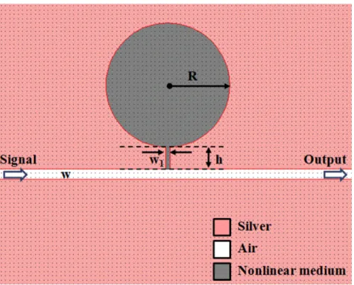
The proposed of single aperture-side-coupled dielectric nano-disk resonators is shown in Fig. 3.1, which is consisted of a waveguide coupled to aperture-side-coupled dielectric nano-disk cavity filling with a Kerr-type nonlinear material. The parameters of the structure are set to be w = 50nm, w1 = 20nm, h = 100nm, and R = 290nm. We
studied the influence of the radius of the nano-cavity on the resonance wavelengths by the FDTD method. The radius is set as variable while the other parameters are fixed as above. Figures 3.2 (a) and (b) show the transmission spectra with different radius R. The resonant peak-wavelengths have a red-shift with increasing of the radius. Fig. 3.2 (a) shows the different radius R=250nm to 370nm and the Fig. 3.2 (b) shows the relationship between the resonant trough-wavelength and the radius of nano-cavity is
approximately linear. And the coupled-aperture width is set as variable while the other parameters are fixed as above. Fig. 3.3 (a) and (b) show the transmission spectra with different width w1. The resonant trough-wavelengths have a red-shift with reducing of
the width. Fig 3.3 (a) shows the different width w1=10nm to 50nm and Fig. 3.3 (b)
shows the relationship between the resonant trough-wavelength and the coupled-aperture width w1 of the nano-disk resonators is approximately inversely. Then
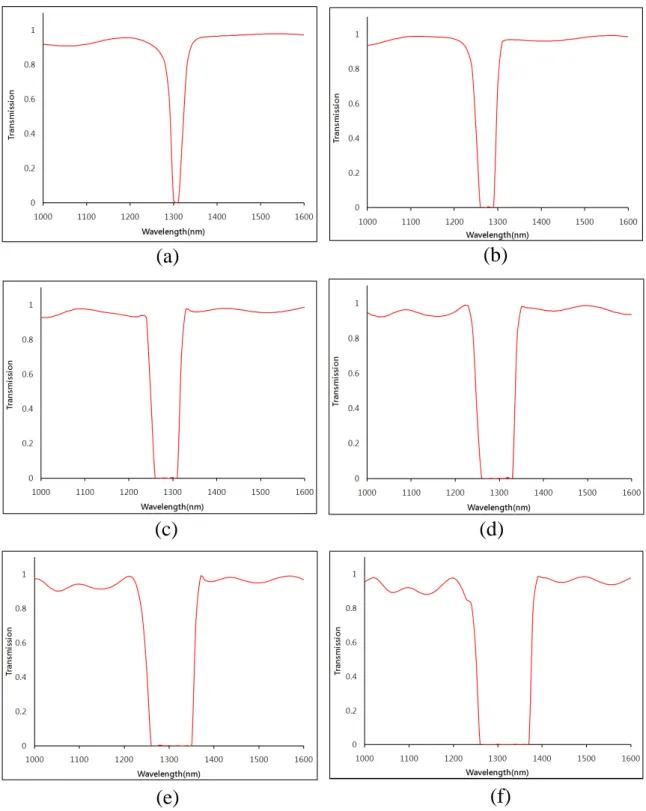
we use the same method to investigate the channel length h between the nano-disk resonators and the bus waveguide. In Figs. 3.4 (a)-(f), the length h is varying from 40nm to 140nm. As the numerical results shown above, the operating wavelength can be easily tuned by changing the radius and the coupled-aperture width of the nano-disk resonator.
Fig.3.5 (a) shows the proposed two nonlinear aperture-coupled dielectric nano-disk resonators. We use the same radii of the nano-disk resonators and two different coupled-aperture width of cavity to find out the influence. The parameters of the proposed structure are setting to be R = 290nm, h = 100nm, d = 240nm, w1 = 20nm, w2
= 30nm, and w = 50nm. According to the above results, the transmission spectra of the output nano-disks possess band-stop wavelengths of 1310nm and 1300nm, respectively. As shown in Fig. 3.5 (b) it is found that the resulting band-stop about 10nm, where the transmission waves through two mirrors generate the destructive interference around the transparency wavelength. Next, we investigate the distance d between the nano-disk cavities. In Figs. 3.6 (a)-(h), the distance d is varied from 0nm to 320nm. When d =240nm, we can get the better band-stop and band-pass results.
investigate the influence of the number of the nano-disk resonators. The number and the radii of the are set as variable while the other parameters are fixed as shown in Tab. 3.1. Figures 3.7(a)-(f) show the transmission spectra with different number of the cavity, the number of cavity are two to twelve. Numerical results of the number of the nano-disk cavity is eight. The best band-pass and the band-stop is eight nano-disk resonators. Next, we analyze AND, OR, NOR, XNOR, NAND and XOR logic gates by using the eight nano-disk resonators filled with a Kerr-type nonlinear material, as shown in Fig. 3.8. Before designing the logic gates, we suit investigate the parameters of the proposed structure to obtain the optimal values for designing the logic devices.
3.3. Simulation and Results
3.3.1. AND gate
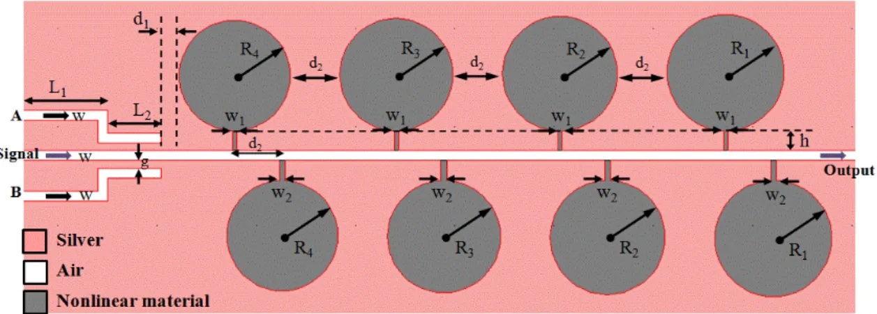
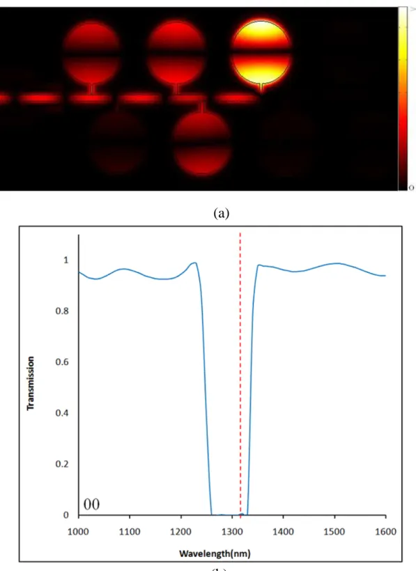
We use the proposed plasmonic waveguide structure with eight-disk resonators filled with a Kerr-type nonlinear material to design an AND logic gate, as shown in Fig. 3.8. Before design the logic gate, we must first investigate the two straight pumping waveguide L1 and L2 and coupling length g the influence. First, we are the proposed
plasmonic waveguide structure, as shown in Fig. 3.8, to design an all-optical AND logic gate. The parameters of the proposed structure are chosen R1 = 295 nm, R2 = 290nm, R3
= 285 nm, R4 = 280 nm, h = 100 nm, w = 50 nm, w1 = 20 nm, w2 = 30 nm, d1 = 20nm,
d2 = 240nm. In the Figure 3.9 and Tab 3.2 shows the band-stop efficiency in wavelength
of 1310nm for different length of pumping waveguide. Basis the simulation results, we found that the best length L1 is 400 nm. Next, we change L2 from 100nm to 500nm. In
wavelength at 1310nm minimum transmittance is 0.002%. Next, we investigate the distance d1 between the nano-disk cavities and waveguide. In Figs. 3.11, the distance d1
is varying from 0nm to 220nm. When d1 =20nm, we can get the better band-stop and
band-pass results. Then we use the same method to investigate the transmission spectra for different gap distance between the straight pumping waveguide and the bus waveguide. In Fig. 3.12 shows that when g = 50nm, we can obtain the best band-pass transmission efficiency. In this structure, the signal port is always ON with the input intensity I0=1x10⁶ V2/m2.
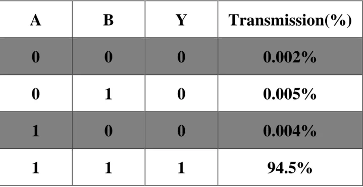
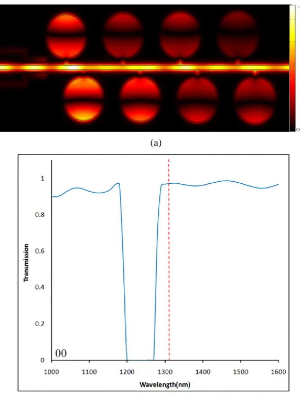
When the control ports A and B are both OFF, the output port is OFF. The magnetic field distribution is shown in Fig. 3.13 (a). The normalized transmission efficiency at the wavelength 1310nm is about 0.002% as shown in Fig. 3.13 (b). When the control port A is OFF, with the input light intensity I1=5x10⁷ V2/m2 and the control port B is ON,
the output port is OFF. The magnetic field distribution is shown in Fig.3.14 (a). The transmission efficiency at the wavelength 1310nm is about 0.005%, as shown in Fig. 3.14 (b). When the control port A is ON and the control port B is OFF, with the input light intensity I1=5x10⁷ V2/m2, the output port is OFF. The magnetic field distribution is
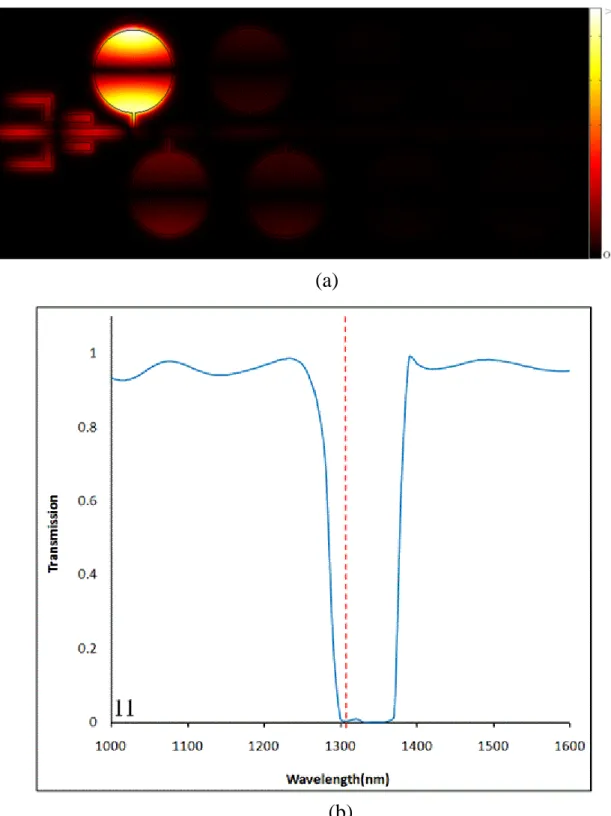
shown in Fig. 3.15 (a). The transmission efficiency at the wavelength 1310nm is about 0.004%, as shown in Fig. 3.15 (b). When both the control ports A and B are ON with the input light intensity I1=5x10⁷ V2/m2, the output port is ON. The magnetic field
distribution is shown in Fig. 3.16 (a). The normalized transmission efficiency at the wavelength 1310nm is about 94.5%, as shown in Fig.3.16 (b). The truth table and the transmission efficiency are shown in Tab. 3.4.
3.3.2. OR Logic gate
We use the proposed plasmonic waveguide structure with eight-disk resonators filled with a Kerr-type nonlinear material to design an OR logic gate, as shown in Fig. 3.8. The parameters of the proposed structure are chosen R1 = 295 nm, R2 = 290nm, R3 =
285 nm, R4 = 280 nm, h = 100 nm, w = 50 nm, w1 = 20 nm, w2 = 30 nm, d2 = 240nm,
L1 = 400nm, L2 = 300nm, g = 60nm. Next, we change the input intensity to achieve the
OR logic gate. In this stage, signal port is always ON with the input light intensity I0=1x10⁶ V2/m2. When the control ports A and B are both OFF, the output port is OFF.
The magnetic field distribution is shown in Fig. 3.17 (a). The transmission efficiency at the wavelength 1310nm is about 0.002%, as shown in Fig. 3.17 (b). When the control port A is OFF and the control port B is ON, with the input light intensity I1=1x10⁸
V2/m2, the output port is ON. The magnetic field distribution is shown in Fig. 3.18 (a). The transmission efficiency at the wavelength 1310nm is about 94.5%, as shown in Fig. 3.18 (b). When the control port A is ON, with the input light intensity I1=1x10⁸ V2/m2
and the control port B is OFF, the output port is ON. The magnetic field distribution is shown in Fig. 3.19 (a). The transmission efficiency at the wavelength 1310nm is about 94.3%, as shown in Fig. 3.19 (b). When both the control ports A and B are ON, with the input light intensity I1=1x10⁸ V2/m2, the output port is ON. The magnetic field
distribution is shown in Fig.3.20 (a). The transmission efficiency at the wavelength 1310nm is about 95.4%, as shown in Fig.3.20 (b). The truth table and the transmission efficiency are shown in Tab. 3.5.
3.3.3. NOR Logic gate
filled with a Kerr-type nonlinear material to design an NOR logic gate, as shown in Fig. 3.8. The parameters of the proposed structure are chosen R1 = 280 nm, R2 = 275nm, R3
= 270 nm, R4 = 265 nm, h = 100 nm, w = 50 nm, w1 = 20 nm, w2 = 30 nm, d2 = 240nm,
L1 = 400nm, L2 = 300nm, g = 60nm. In this stage, signal port is always ON with the
input light intensity I0=1x10⁶ V2/m2. When the control ports A and B are both OFF, the
output port is ON. The magnetic field distribution is shown in Fig. 3.21 (a). The transmission efficiency at the wavelength 1310nm is about 97.4%, as shown in Fig. 3.21 (b). When the control port A is OFF and the control port B is ON, with the input light intensity I1=5x10⁷ V2/m2, the output port is OFF. The magnetic field distribution is
shown in Fig. 3.22 (a). The transmission efficiency at the wavelength 1310nm is about0.005%, as shown in Fig. 3.22 (b). When the control port A is ON, with the input light intensity I1=5x10⁷ V2/m2 and the control port B is OFF, the output port is OFF. The
magnetic field distribution is shown in Fig. 3.23 (a). The transmission efficiency at the wavelength 1310nm is about 0.006%, as shown in Fig. 3.23 (b). When both the control ports A and B are ON, with the input light intensity I1=5x10⁷ V2/m2, the output port is
OFF. The magnetic field distribution is shown in Fig.3.24 (a). The transmission efficiency at the wavelength 1310nm is about 0.007%, as shown in Fig.3.24 (b). The truth table and the transmission efficiency are shown in Tab. 3.6.
3.3.4. XNOR Logic gate
We use the proposed plasmonic waveguide structure with eight-disk resonators filled with a Kerr-type nonlinear material to design an XNOR logic gate, as shown in Fig. 3.8. The parameters of the proposed structure are chosen R1 = 280 nm, R2 = 275nm,
240nm, L1 = 400nm, L2 = 300nm, g = 60nm. Next, we change the input intensity to
achieve the XNOR logic gate. In this stage, signal port is always ON with the input light intensity I0=1x10⁶ V2/m2. When the control ports A and B are both OFF, the output port
is ON. The magnetic field distribution is shown in Fig. 3.25 (a). The transmission efficiency at the wavelength 1310nm is about 97.4%, as shown in Fig. 3.25 (b). When the control port A is OFF and the control port B is ON, with the input light intensity I1=1x10⁸ V2/m2, the output port is OFF. The magnetic field distribution is shown in Fig.
3.26 (a). The transmission efficiency at the wavelength 1310nm is about0.004%, as shown in Fig. 3.26 (b). When the control port A is ON, with the input light intensity I1=1x10⁸ V2/m2 and the control port B is OFF, the output port is OFF. The magnetic
field distribution is shown in Fig. 3.27 (a). The transmission efficiency at the wavelength 1310nm is about 0.005%, as shown in Fig. 3.27 (b). When both the control ports A and B are ON, with the input light intensity I1=1x10⁸ V2/m2, the output port is
ON. The magnetic field distribution is shown in Fig.3.28 (a). The transmission efficiency at the wavelength 1310nm is about 94.6%, as shown in Fig.3.28 (b). The truth table and the transmission efficiency are shown in Tab. 3.7.
3.3.5. NAND Logic gate
We use the proposed plasmonic waveguide structure with eight-disk resonators filled with a Kerr-type nonlinear material to design an NAND logic gate, as shown in Fig. 3.8. The parameters of the proposed structure are chosen R1 = 270 nm, R2 = 265nm,
R3 = 260 nm, R4 = 255 nm, h = 100 nm, w = 50 nm, w1 = 20 nm, w2 = 30 nm, d2 =
240nm, L1 = 400nm, L2 = 300nm, g = 60nm. In this stage, signal port is always ON
OFF, the output port is ON. The magnetic field distribution is shown in Fig. 3.29 (a). The transmission efficiency at the wavelength 1310nm is about 97.3%, as shown in Fig. 3.29 (b). When the control port A is OFF and the control port B is ON, with the input light intensity I1=5x10⁷ V2/m2, the output port is ON. The magnetic field distribution is
shown in Fig. 3.30 (a). The transmission efficiency at the wavelength 1310nm is about 96.1%, as shown in Fig. 3.30 (b). When the control port A is ON, with the input light intensity I1=5x10⁷ V2/m2 and the control port B is OFF, the output port is ON. The
magnetic field distribution is shown in Fig. 3.31 (a). The transmission efficiency at the wavelength 1310nm is about 96.2 %, as shown in Fig. 3.31 (b). When both the control ports A and B are ON, with the input light intensity I1=5x10⁷ V2/m2, the output port is
OFF. The magnetic field distribution is shown in Fig.3.32 (a). The transmission efficiency at the wavelength 1310nm is about 0.002% as shown in Fig.3.32 (b). The truth table and the transmission efficiency are shown in Tab. 3.8.
3.3.6. XOR Logic gate
Finally, we use the proposed plasmonic waveguide structure with eight-disk resonators filled with a Kerr-type nonlinear material to design an XOR logic gate, as shown in Fig. 3.8. The parameters of the proposed structure are chosen R1 = 295 nm, R2
= 290nm, R3 = 265 nm, R4 = 260 nm, h = 100 nm, w = 50 nm, w1 = 20 nm, w2 = 30 nm,
d2 = 240nm, L1 = 400nm, L2 = 300nm, g = 60nm. In this stage, signal port is always ON
with the input light intensity I0=1x10⁶ V2/m2. When the control ports A and B are both
OFF, the output port is OFF. The magnetic field distribution is shown in Fig. 3.33 (a). The transmission efficiency at the wavelength 1310nm is about 0.002% as shown in Fig. 3.33 (b). When the control port A is OFF and the control port B is ON, with the input
light intensity I1=6x10⁷ V2/m2, the output port is ON. The magnetic field distribution is
shown in Fig. 3.34 (a). The transmission efficiency at the wavelength 1310nm is about97.3%, as shown in Fig. 3.34 (b). When the control port A is ON, with the input light intensity I1=6x10⁷ V2/m2 and the control port B is OFF, the output port is ON. The
magnetic field distribution is shown in Fig. 3.35 (a). The transmission efficiency at the wavelength 1310nm is about 96.8 %, as shown in Fig. 3.35 (b). When both the control ports A and B are ON, with the input light intensity I1=6x10⁷ V2/m2, the output port is
OFF. The magnetic field distribution is shown in Fig.3.36 (a). The transmission efficiency at the wavelength 1310nm is about 0.002%, as shown in Fig.3.36 (b). The truth table and the transmission efficiency are shown in Tab. 3.9.
3.4. Summary
In this chapter, we have numerically investigated the all-optical plasmonic logic gate based on the nano-disk cavity structures filled with optical nonlinear Kerr material. At first, we investigated the radius of the disk resonators. We find that the larger radius we set, the longer wavelength peak wavelength shifts. Conversely the resonant peak-wavelength and the coupled-aperture width of the nano-disk resonators are approximately inversely. We can easily filter out the desired wavelength by properly adjusting the radii and the coupled-aperture width of the nano-disk resonators. According to this result, we can choose the operating wavelength by adjusting the radii of the nano-disk resonators, coupled-aperture width or the pump light. For the proposed all-optical AND gates, the normalized transmission efficiencies of the high logic state and the low logic state are about 94.5% and 0.002%, respectively. Then, we increase the
pumping light intensity to achieve the OR logic gate. The proposed OR gate normalized transmission of high logic state is about 95.4% and low logic state is 0.002%. Next, we changed the radius of disk resonators to achieve the NOR logic gate. The proposed NOR gates normalized transmission efficiency of high logic state is about 97.4% and low logic state is 0.005%. Then, we increased the pumping light intensity to achieve the XNOR logic gate. The proposed XNOR gate normalized transmission of high logic state is about 97.4% and low logic state is 0.004%. Next, we changed the radius of disk resonators to achieve the NAND logic gate. The proposed NAND gates normalized transmission efficiency of high logic state is about 97.3% and low logic state is 0.002%. Finally, we use two groups the radius of disk resonators to achieve the XOR logic gate. The proposed XOR gates normalized transmission efficiency of high logic state is about 97.3% and low logic state is 0.002%. According to the numerical results, the proposed MIM plasmonic.
Fig. 3.2 Transmission spectra of the single disk cavity structure with different radius of R, (a) R=250nm~370nm and (b) Relationship between the resonance wavelength and radius of the nano-disk cavity.
(a)
Fig. 3.3 Transmission spectra of the coupled-aperture with different width of w1, (a)
R=10nm~50nm and (b) Relationship between the resonant trough-wavelength and the coupled-aperture width w1 of the nano-disk resonators
(a)
Fig. 3.4 The normalized transmission spectra for fixed R = 290nm, w1 = 20nm, w =
50nm with different h (a) 40nm, (b) 60nm, (c) 80nm, (d) 100nm, (e) 120nm, and (f) 140nm.
(a)
(b)
(c)
(d)
Fig. 3.5 (a)Two nonlinear aperture-side-coupled dielectric nano-disk resonators. (b) The normalized transmission spectrum of the filter.
(a)
Fig. 3.6 The normalized transmission spectra for fixed R = 290nm, h = 100nm, w1 =
20nm, w2 = 30nm and w = 50nm with different d (a) 0nm, (b) 20nm, (c) 40nm,
(d) 60nm, (e) 80nm, (f) 160nm, (g) 240nm, (h) 320nm.
(a)
(b)
(c)
(e)
(f)
(d)
(g)
(h)
Tab. 3.1 The number of the cavity and radius are set as variable while the other parameters are fixed h = 100nm, w1 = 20nm, w2 = 30nm, w = 50nm and d=
Fig. 3.7 The normalized transmission spectra for fixed h= 100nm, w1= 20nm, w2 =
30nm and d=240nm with different number of cavity(a) two-cavity, (b) four- cavity, (c) six-cavity, (d) eight-cavity, (e) ten-cavity, and (f) twelve-cavity.
(a)
(b)
(c)
(d)
Fig. 3.9 The transmission efficiencies of different L1: 200nm to 600nm.
Tab. 3.2 The band-stop efficiencies at wavelength 1310nm for different L1:200nm to
600nm.
L1(nm) 200nm 300nm 400nm 500nm 600nm
Fig. 3.10 The transmission efficiencies of different L2: 100nm to 500nm.
Tab. 3.3 The band-stop efficiencies at wavelength 1310nm for different L2:100nm to
500nm.
L2(nm) 100nm 200nm 300nm 400nm 500nm
Fig. 3.13 When A=0、B=0, (a) the magnetic field distribution and (b) the normalized transmissions of the proposed AND logic gate.
(a)
Fig. 3.14 When A=0、B=1, (a) the magnetic field distribution and (b) the normalized transmissions of the proposed AND logic gate.
(a)
Fig. 3.15 When A=1、B=0, (a) the magnetic field distribution and (b) the normalized transmissions of the proposed AND logic gate.
(a)
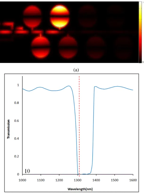
Fig. 3.16 When A=1、B=1, (a) the magnetic field distribution and (b) the normalized transmissions of the proposed AND logic gate.
(a)
Tab. 3.4 The truth table of the proposed AND logic gate.
A
B
Y
Transmission(%)
0
0
0
0.002%
0
1
0
0.005%
1
0
0
0.004%
1
1
1
94.5%
Fig. 3.17 When A=0、B=0, (a) the magnetic field distribution and (b) the normalized transmissions of the proposed OR logic gate.
(a)
Fig. 3.18 When A=0、B=1, (a) the magnetic field distribution and (b) the normalized transmissions of the proposed OR logic gate.
(a)
Fig. 3.19 When A=1、B=0, (a) the magnetic field distribution and (b) the normalized transmissions of the proposed OR logic gate.
(a)
Fig. 3.20 When A=1、B=1, (a) the magnetic field distribution and (b) the normalized transmissions of the proposed OR logic gate.
(b)
(a)
Tab. 3.5 The truth table of the proposed OR logic gate.