Electron emission properties of relaxation-induced traps in InAs/GaAs quantum dots
and the effect of electronic band structure
J. F. Chen and J. S. Wang
Citation: Journal of Applied Physics 102, 043705 (2007); doi: 10.1063/1.2770817
View online: http://dx.doi.org/10.1063/1.2770817
View Table of Contents: http://scitation.aip.org/content/aip/journal/jap/102/4?ver=pdfcov Published by the AIP Publishing
Articles you may be interested in
Characterization of electron emission from relaxed InAs quantum dots capped with InGaAs J. Appl. Phys. 98, 013716 (2005); 10.1063/1.1957124
Carrier distribution and relaxation-induced defects of InAs/GaAs quantum dots Appl. Phys. Lett. 77, 3027 (2000); 10.1063/1.1323735
Characterization of electron trap states due to InAs quantum dots in GaAs Appl. Phys. Lett. 76, 2916 (2000); 10.1063/1.126516
Observation of carrier depletion and emission effects on capacitance dispersion in relaxed In 0.2 Ga 0.8 As/GaAs quantum wells
Appl. Phys. Lett. 75, 2461 (1999); 10.1063/1.125048
Electrical characterization of partially relaxed In x Ga 1x As /GaAs multiple quantum well structures Appl. Phys. Lett. 70, 3284 (1997); 10.1063/1.118428
GaAs layer and a misfit-dislocation-related trap near the QD. The threading trap decreases its electron-emission energy from 0.63 to 0.36 eV from sample surface toward the QD, whereas the misfit trap gradually increases its electron-emission energy from 0.28 to 0.42 eV from near the QD toward the GaAs bottom layer, indicating that both traps near the QD have lower electron-emission energies. Hence, the emission-energy change is attributed to the related traps across the QD interface where a band offset exists. The C-V profiling at 300 K shows extended carrier depletion near the QD. As temperature is increased, an electron-emission peak emerges at the QD followed by a prominent peak, suggesting that the trap responsible for the prominent peak lies in energy below the QD electron ground state. From a simulation, this trap is identified to be the misfit trap located at the QD and at the observed emission energy below the GaAs conduction band. Based on the energy location of this trap, we deduce a possible mode of strain relaxation. © 2007 American Institute of
Physics.关DOI:10.1063/1.2770817兴
I. INTRODUCTION
InAs/GaAs self-assembled quantum dots1–9 共QDs兲 have recently attracted considerable attention for both theoretical and experimental studies due to promising technological applications.10–14 Many works have focused on experimen-tally determining the electronic band structure of the QD 共Refs. 15–20兲 by analyzing electron emission from the QD.
However, this emission time is very short and difficult to resolve probably due to the presence of significant tunneling.15,19,20 On the other hand, deep traps with their strongly localized wave functions have been proposed as lo-cal probes for characterizing electronic band structure.22–24 When InAs thickness is increased beyond the critical thick-ness共⬃3 ML兲,21strain is relaxed by the formation of misfit dislocations confined near relaxation interface. This trap was previously shown to be point-defect-like25 because its capacitance-time transience exhibits an exponential function. Hence, it would be worthwhile to explore the possibility of using this trap as a probe. Furthermore, understanding the electron-emission properties of this trap may also provide valuable information on strain relaxation. Therefore, in this work, the electron-emission properties of relaxation-induced traps in InAs QDs are investigated in detail by using capacitance-voltage共C-V兲 profiling and deep-level transient spectroscopy共DLTS兲 with small step voltages.
Among many electrical characterizations, DLTS is very convenient for evaluating the carrier-emission properties of defect traps. However, when the probed sample is not of a simple bulk structure, analyzing DLTS spectra is difficult because the emission parameters are affected by band
struc-ture, and thus bias dependent. This task is even more difficult when multiple traps are present. This work has demonstrated an important effect of electronic band structure. Selecting a small step voltage was necessary to resolve the DLTS spectra of relaxation-induced traps. Aided by C-V profiling at el-evated temperatures and a band structure simulation, we were able to obtain important information on the electron-emission parameters of two traps related to threading and misfit dislocations, respectively.
II. EXPERIMENTS
The InAs/GaAs QD samples studied here were grown on
n+-GaAs 共100兲 substrates by solid source molecular beam epitaxy in a Riber Epineat machine. The QDs were formed in Stranski–Krastanow growth mode by depositing the InAs layer at 490 ° C. The QDs structure is sandwiched between two 0.3 m-thick Si-doped GaAs 共⬃6⫻1016 cm−3兲 layers for electrical characterizations. Detailed growth of the QD samples can be found elsewhere.26A typical QD sheet den-sity about 3⫻1010 cm−2 was observed by atomic force mi-croscopy images. Schottky diodes were realized by evaporat-ing Al on sample surface with a dot diameter of 1500 m. Photoluminescence 共PL兲 measurements were carried out us-ing a double frequency yttrium-aluminum-garnet:Nd laser at 532 nm. A HP 4194A gain phase analyzer was used for C-V profiling.
III. MEASUREMENT AND RESULTS A. DLTS spectra of relaxed QDs
In the previous transmission electron microscopy studies,21 strain in InAs QDs was shown to relax by the induction of threading dislocations in the top GaAs layer and
a兲Electronic mail: [email protected]
0021-8979/2007/102共4兲/043705/6/$23.00 102, 043705-1 © 2007 American Institute of Physics [This article is copyrighted as indicated in the article. Reuse of AIP content is subject to the terms at: http://scitation.aip.org/termsconditions. Downloaded to ] IP:
misfit dislocations near the QDs. The threading dislocations which propagate from the QDs to the sample surface are likely generated by the gliding process of interfacial disloca-tions due to elastic strain acting as a shear stress.27,28 In contrast, the misfit dislocations do not propagate into the GaAs layers but are confined near the QD, suggesting a bending of the misfit dislocations toward the QD interface by strain. Similar confinement of misfit dislocations has been observed in relaxed InGaAs/GaAs heterostructures.28
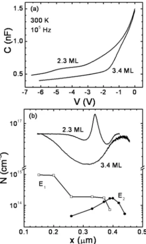
Figures1共a兲and1共b兲show the 300-K C-V and the con-verted concentration profiles of InAs QD samples with InAs thicknesses of 2.3 and 3.4 ML, respectively, measured at 105 Hz. The latter sample is relaxed because the InAs
thick-ness exceeds the critical thickthick-ness of ⬃3 ML.21 While the 2.3 ML sample shows strong electron accumulation, the re-laxed sample exhibits carrier depletion at the dots共0.3 m兲 and neighboring GaAs layers. Hence, strain relaxation must induce electron traps to deplete the QDs. DLTS measure-ments were used to reveal the traps. Figure 2 shows the obtained spectra of the 2.3 and 3.4 ML samples, along with a 1.1 ML InAs sample which is of a quantum-well structure because QD has not formed. The sweeping voltages are as indicated. While the 1.1 and 2.3 ML samples display no traps, the 3.4 ML sample exhibits a broad signal at low tem-perature superimposed upon a background signal, suggesting the presence of significant relaxation-induced traps. Figure3
shows that when step voltage is reduced to −0.5 V 共super-imposed upon a quiescent bias from 0 to −4 V兲, the
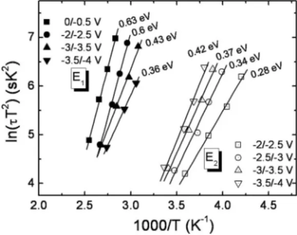
spec-trum can be well resolved into two prominent traps, E1 from 0 / −0.5 to −3.5/ −4 V and E2 from −1 / −1.5 to −4 / −4.5 V. The rate window is 8.6 ms and filling pulse time is set at 30 ms to ensure the peak-height saturation of the E2 trap. As guided by the dash lines, the peak temperature of E1 共E2兲 shifts toward a lower 共higher兲 temperature as reverse bias is increased. This strong bias dependence can explain the broad spectrum in Fig. 2. As shown in Fig. 3, the E2 traps for −1 / −1.5 and −1.5/ −2 V are rather asymmetric with a broad low-temperature tail, and thus their emission energies cannot be determined accurately. Figure4shows the corresponding Arrhenius plots of the traps, from which the activation ener-gies and capture cross sections are obtained.
Given the DLTS spectra in Fig.3 and the C-V curve in Fig.1共a兲, the concentrations and spatial locations of the traps
FIG. 1. 共a兲 300-K C-V and 共b兲 concentration profiles measured at 105 Hz
for the nonrelaxed 2.3 ML and relaxed 3.4 ML samples. Strain relaxation causes carrier depletion near the dot共0.3 m兲 and neighboring GaAs layers by the generation of two traps, E1 and E2, related to the threading and misfit dislocations, respectively. Their concentrations, determined from the DLTS spectra in Fig.3, show that the E1 trap is located in the top GaAs layer and the E2 trap is located near the QD.
FIG. 2. DLTS spectra of the 1.1 ML InAs quantum-well sample, nonrelaxed 2.3 ML, and relaxed 3.4 ML InAs QDs samples under various sweeping voltages as indicated. Strain relaxation causes a broad signal at low tem-peratures superimposed on a high-temperature background signal, which can be resolved into two major traps in Fig. 3when a small step voltage is selected.
FIG. 3. DLTS spectra of the relaxed 3.4 ML sample, showing two traps; the E1 trap is associated with the threading dislocations in the top GaAs layer and the E2 trap is associated with the misfit dislocations near the QD. With increasing reverse quiescent bias, the peak temperature of the E1共E2兲 trap shifts toward a lower 共higher兲 temperature, reflecting smaller electron-emission energies for both the traps near the QD. This effect is attributed to the related traps across the QD interface where a band offset locates. The E2 spectra from −1 / −1.5 to −2.5/ −3 V is asymmetric with a very broad low-temperature tail, suggesting the presence of continuous energy states below the GaAs CB edge, to which electrons are emitted from the E2 trap. The continuous states are attributed to the QD electron states.
043705-2 J. F. Chen and J. S. Wang J. Appl. Phys. 102, 043705共2007兲
are evaluated, as shown in Fig. 1共b兲. The concentration is determined from the expression共2⌬C/C兲N, where ⌬C is the peak intensity of the related trap and N is the background concentration 6⫻1016 cm−3. The spatial location is simply obtained from the edge of depletion region共EOD兲 from the
C-V curve. For example, for the E1 trap observed in 0 /
−0.5 V, a middle bias −0.25 V is used to find the EOD. A trap will donate carriers only when Fermi level crosses it. However, at this point, due to the energetic depth of the trap, the EOD is deeper than the crossing point, and thus the ob-tained location is deeper than the actual location of the trap. From a simple simulation共to be shown兲, a trap that is located at the QDs 共0.3 m兲 and at 0.35 eV below the GaAs conduction-band共CB兲 edge will show its emission signal at 0.39 m. Thus, the depth 0.39 m in Fig. 1共b兲 can be roughly treated as the location of the QDs. Hence, the E1 trap is located from the sample surface to a depth near the QDs. Its concentration gradually decreases from the surface toward the QD. This spatial distribution correlates with that of the threading dislocations, and thus the E1 trap is attrib-uted to the threading dislocations. The E2 trap is located in the vicinity of the QDs; its concentration gradually increases from the top GaAs layer near the QDs, reaches a maximum at the QD, and then rapidly decreases toward the lower GaAs layer. This spatial distribution leads us to attribute the E2 trap to the misfit dislocations.
B. Properties of the threading trap
As shown in Figs.3and4, the electron-emission energy of the E1 trap decreases from 0.63 eV 共␣= 3.9 ⫻10−15 cm−2兲 for 0/−0.5 V to 0.36 eV 共= 1.9
⫻10−16 cm−2兲 for −3.5/−4 V, suggesting a smaller
electron-emission energy near the QDs. The DLTS peak height of this trap shows no saturation even when filling pulse duration time is increased to 100 ms. This feature is consistent with the capacitance-time transience of the traps associated with threading dislocations, which exhibits a loga-rithmic function,27,28 characteristic of Coulombic repulsion of the carriers captured at the traps along with the linearly arrayed dislocation lines.27 This trap is believed to be the ED1 共0.68 eV兲, reported by Wosinski27 from studying
plas-tically deformed GaAs, and the trap at 0.58 eV observed in InGaAs/GaAs by Watson et al.29who assigned it to the cores of ␣-type dislocations. The electron-emission energy ob-tained by Watson et al.29 is smaller than that by the Wosinski27. Watson et al.29 explained this by the threading dislocations in the InGaAs side which has a smaller band gap, as relative to GaAs. He suggested that the trap was probably tied to the valence-band edge and thus the emission-energy difference might be the band gap difference between GaAs and InGaAs. This band structure effect can explain the decrease of the electron-emission energy of the E1 trap. A trap generally decreases its emission energy as the band gap of the host material is reduced. For example, Irvine and Palmer30 have shown an electron-emission-energy de-crease in EL2 from 0.84 to 0.62 as x inde-creases from 0 to 0.18 for an InxGa1−xAs layer grown on GaAs. Hence, the
electron-emission-energy change may reflect the energy band struc-ture of the host material. Further investigation is needed to make a quantitative argument.
C. C-V profiling at elevated temperatures
As Fig. 1共b兲 is shown, the QD in the relaxed 3.4 ML sample is depleted of electrons. This depletion is presumably caused by the E2 trap which must lie in energy below the QD electron ground state. Due to the long emission time, elec-trons trapped on the E2 trap cannot follow the alternating current 共ac兲 signal to be modulated. This depletion remains as frequency is lowered to 200 Hz. However, one may di-rectly activate the electron emission from the trap by increas-ing temperature to reduce the emission time. Figure5shows the C-V and the corresponding depth profiles共in the inset兲 at 370 K. The profile shows similar carrier depletion at 105 Hz;
however, at 200 Hz, a C plateau at around −3 V and a C protrusion at around −4.5 V emerge. The C plateau is con-verted to a carrier-accumulation peak centered at 0.33 m. This depth is close to the location共0.34 m兲 of the carrier-accumulation peak in the nonrelaxed 2.3 ML sample关in Fig.
1共b兲兴, and thus the peak is considered as electron emission from the QD electron states and is designated as quantum emission 共QE兲. The presence of the QD electron states can
FIG. 4. Arrhenius plots of the E1 and E2 traps at different sweeping volt-ages. The electron-emission energies are also indicated in the DLTS spectra in Fig.3.
FIG. 5. C-V spectra and the corresponding concentration profiles共in the inset兲 of the relaxed 3.4 ML sample, measured at 370 K. When frequency is reduced to 200 Hz, the C-V spectra show a C plateau, corresponding to an electron-emission peak at the QD, and a C protrusion, corresponding to electron emission from the E2 trap.
be justified from the 10-K PL spectra in Fig.6of the nonre-laxed 2.3 ML and the renonre-laxed 3.4 ML samples. The 2.3 ML sample shows a QD ground emission at 1.13 eV which is redshifted to 1.1 eV in the 3.4 ML sample presumably due to an increase in dot size. The peak of the 3.4 ML sample is only slightly broader than that of the 2.3 ML sample, sug-gesting that strain relaxation does not destroy the QD elec-tron ground state. Kapteyn et al.15 reported a value of 0.19 eV for the confinement energy of InAs QD electron ground state for an QD ground emission at 1.12 eV, a value close to the emission energy of the 3.4 ML sample. Thus, the QD electron ground state is placed at 0.19 eV below the GaAs CB edge, as shown in the simplified schematic CB diagram in Fig. 6. Neglecting the effect of band structure, the ener-getic locations of the E1 and E2 traps are also illustrated.
D. Depth-profile simulation of the misfit trap
As to the C protrusion at −4.5 V 共in Fig.5兲, it may be
due to the electron emission from the E2 trap. From the DLTS data, the emission rate of the E2 trap共at 0.37 eV for −3 / −3.5 V兲 can be extrapolated to 1.7⫻103 Hz at 370 K
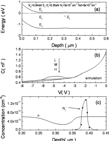
which is larger than the ac modulating frequency of 200 Hz, allowing for the E2 trap to be modulated. This C protrusion is seen after the QE peak, suggesting that the E2 trap lies below the QD electron ground state, consistent with the carrier-depletion effect. To see what energy level the electron-emission energy is relative to, we simulate C-V pro-file by solving the Poisson equation for a n-type GaAs Schottky diode 共a barrier height of 0.84 eV兲 with a back-ground doping of 6⫻1016 cm−3 and an acceptor trap of 3 ⫻1017 cm−3at the QD共0.3 m兲 with a thickness of 10 nm
共equivalent to a sheet concentration of 3⫻1011 cm−2兲 and at
0.35 eV below the GaAs CB edge, as shown in Fig. 7共a兲. Figure 7共b兲 shows the simulated C-V profiles under three conditions: the L curve represents a low ac frequency so that the trapped electron can be modulated, the M curve repre-sents a medium frequency so that the trapped electron cannot
follow the ac signal but can follow the direct current 共dc兲 sweeping rate, and the H curve represents that the trapped electron cannot even follow the dc sweeping rate 共this con-dition is not satisfied during the experiment兲. As shown, the
L and M curves are in general agreement with the
experi-mental curves in Fig. 5 under 200 共neglecting QE plateau兲 and 105 Hz, respectively. Figure 7共c兲 shows the simulated
depth profile in the M condition, illustrating carrier depletion at around 0.3 m which is in fair agreement with the experi-mental carrier depletion in Fig. 1共b兲. Figure7共c兲also shows the simulated concentration profile of the E2 trap using the same equation,共2⌬C/C兲N as used in Fig.1共b兲, except⌬C is taken from the difference between the L and M curves. The spatial location of the E2 trap is obtained from the M curve, which shows a nearly constant C 共0.55 nF兲 for the observa-tion of the C protrusion in the L curve. This constant C yields an EOD depth of 0.38 m which is in fair agreement with the maximum concentration 共0.39 m兲 of the E2 trap in Fig.1共b兲. Therefore, the carrier depletion is mainly due to the E2 trap that is located at the QDs and at 0.37 eV below the GaAs CB edge. Note that the simulated C protrusion starts at −3 V; however, the DLTS spectra show the E2 trap starting from −1 / −1.5 V. Thus, E2 trap probably spread into the top GaAs layer near the QDs.
FIG. 6. 10-K PL spectra of the nonrelaxed 2.3 and relaxed 3.4 ML QD samples, showing a redshift of the QD ground emission. Strain relaxation does not severely degrade the QD quality. Also included is a schematic CB diagram showing the QD electron ground state共at 0.19 eV below the GaAs CB edge兲 and energetic and spatial locations of the threading trap E1 and misfit trap E2. For simplicity, the effect of electronic band structure on the electron-emission energies of both traps is not shown.
FIG. 7.共a兲 Energy band diagram used for simulation, assuming the presence of a trap with a concentration of 3⫻1017 cm−3, located near the QD with a
thickness of 10 nm and at 0.35 eV below the GaAs CB edge.共b兲 Simulated
C-V spectra under three conditions depending upon ac frequency and dc
sweeping rate: the L curve represents that the trapped electron can follow ac signal, the M curve represents that the trapped electron cannot follow ac signal but can follow dc sweeping rate, and the H curve represents that the trapped electron cannot even follow dc sweeping rate.共c兲 Simulated con-centration profile without any trap emission共in the M condition兲 and con-centration profile of electron emission from the E2 trap.
043705-4 J. F. Chen and J. S. Wang J. Appl. Phys. 102, 043705共2007兲
al. claimed that this trap was a monolevel trap because its capture cross section was temperature independent. Recently, Yastrubchak et al.31 reported an exponential function for a misfit-related hole trap in InGaAs/GaAs heterostructures. This trap was claimed to have a higher regularity as com-pared with threading dislocations. Since the E2 trap is likely a point defect and is at 0.37 eV below the GaAs CB edge, we compare it with point defects in GaAs. In terms of its energy location, it is likely EL6共Ec− 0.35 eV兲 共Ref.32兲 observed in
low-temperature grown GaAs, commonly considered as
VGa-Asi complex. If it is indeed VGa-Asi, we can deduce a
likely mode of strain relaxation. Due to underlying GaAs layer, the deposited InAs QDs are compressed laterally. At the onset of relaxation, the compressive stress in the QDs is relieved probably by the displacement of As atoms from their lattice sites, leading to excess As in the form of Asinear the
QD. These Asimay react with the misfit dislocations to
pro-duce Ga vacancies 共VGa兲 by the interaction30: Asi
+ dislocation→dislocation climb +VGa. After that, the
in-duced VGamay interact with residual Asi and form Asi-VGa
complex, leading to the spatial correlation between the E2 trap and misfits.
As Fig.3shown, the electron-emission energy of the E2 trap increases from 0.28 to 0.42 eV as sweeping voltage increases from −2 / −2.5 to −3.5/ −4 V. Additionally, the E2 spectra from −1 / −1.5 to −2.5/ −3 V共corresponding to a re-gion near the QDs兲 contain a very broad low-temperature tail. The bias dependence of the electron-emission energy cannot be explained by a field-enhanced tunneling, since in-creasing the amplitude of bias would enhance emission rate and reduce electron-emission energy. This bias dependence seems to suggest a rather broad energy spectrum of the E2 trap. However, the E2 trap at 0.37 eV for −3 / −3.5 V, as well as for −3.5/ −4 V, is quite symmetric and narrow in line-width. Also, from the simulation, electrons are emitted to the GaAs CB for these sweeping voltages. Thus, we explained the lower electron-emission energy and the low-temperature tail共from −1/−1.5 to −2.5/−3 V兲 as an effect of band struc-ture. Continuous energy states may exist below the GaAs CB edge to which electrons trapped on the E2 traps are emitted. Since they are observed in a region near the QD, the con-tinuous states are considered as the QD electron states. Note that this trend is similar as the E1 trap; both traps show smaller electron-emission energies for a region near the QDs. Strain relaxation is expected to enhance fluctuation of the QD states, leading to a smearing of emission energies and formation of tails. The results of the present studies illustrate a significant effect of electronic band structure on the
its electron-emission energy from 0.63 to 0.36 eV from the sample surface toward the QD. This is explained by the trap across the QD interface where a band offset exists. By per-forming C-V profiling at elevated temperatures, we observe a
C plateau followed by a C protrusion; the plateau is
identi-fied as the electron emission from the QD and the protrusion as the electron emission from a defect trap. A simple simu-lation establishes that the defect trap is the misfit trap located at 0.37 eV below the GaAs conduction-band edge. In terms of its emission energy, this misfit trap is ascribed to EL6, commonly considered as VGa-Asi complex. As the E1 trap,
the emission energy of the E2 trap shows a smaller electron-emission energy and a broad low-temperature tail for a re-gion near the QD.
ACKNOWLEDGMENTS
The authors gratefully acknowledge the National Sci-ence Council of Taiwan for financially supporting this re-search under Contract No. NSC-95-2112-M-009-010 and MOE, ATU program.
1F. Heinrichsdorff, M.-H. Mao, N. Kirstaedter, A. Krost, and D. Bimberg,
Appl. Phys. Lett. 71, 22共1997兲.
2T. E. Nee, N. T. Yeh, P. W. Shiao, J. I. Chyi, and C. T. Lee, Jpn. J. Appl.
Phys., Part 1 38, 605共1999兲.
3D. J. Eaglesham and M. Cerullo, Phys. Rev. Lett. 64, 1943共1990兲. 4D. Leonard, K. Pond, and P. M. Petroff, Phys. Rev. B 50, 11687共1994兲. 5S. Guha, A. Madhukar, and K. C. Rajkumar, Appl. Phys. Lett. 57, 2110
共1990兲.
6J. M. Moison, F. Houzay, F. Barthe, and L. Leprince, Appl. Phys. Lett. 64,
196共1994兲.
7D. J. Bottomley, Appl. Phys. Lett. 72, 783共1998兲.
8C. W. Snyder, J. F. Mansfield, and B. G. Orr, Phys. Rev. B 46, 9551
共1992兲.
9D. Leonard, M. Krishnamurthy, C. M. Reaves, S. P. Denbaars, and P. M.
Petroff, Appl. Phys. Lett. 63, 3203共1993兲.
10H. Shoji, K. Mukai, N. Ohtsuka, M. Sugawara, T. Uchida, and H.
Ish-ikawa, IEEE Photonics Technol. Lett. 7, 1385共1995兲.
11G. Yusa and H. Sakaki, Electron. Lett. 32, 491共1996兲.
12N. Yokoyama, S. Muto, K. Imamura, M. Takatsu, T. Mori, Y. Sugiyama,
Y. Sakuma, H. Nakao, and T. Adachihara, Solid-State Electron. 40, 505 共1996兲.
13Y. Arakawa and H. Sakaki, Appl. Phys. Lett. 40, 939共1982兲.
14J. C. Campbell, D. L. Huffaker, H. Deng, and D. G. Deppe, Electron. Lett.
33, 1337共1997兲.
15C. M. A. Kapteyn, F. Heinrichsdorff, O. Stier, R. Heitz, M. Grundmann,
and P. Werner, Phys. Rev. B 60, 14265共1999兲.
16R. J. Luyken, A. Lorke, A. O. Govorov, J. P. Kotthaus, G.
Medeiros-Riberro, and P. M. Petroff, J. Appl. Phys. 74, 2486共1999兲.
17X. Letartre, D. Stievenard, and M. Lanoo, J. Appl. Phys. 69, 7336共1991兲. 18H. L. Wang, F. H. Yang, S. L. Feng, H. J. Zhu, D. Ning, H. Wang, and X.
D. Wang, Phys. Rev. B 61, 5530共2000兲.
19J. F. Chen, R. S. Hsiao, C. K. Wang, J. S. Wang, and J. Y. Chi, J. Appl.
Phys. 98, 013716共2005兲.
20W. H. Chang, W. Y. Chen, M. C. Cheng, C. Y. Lai, T. M. Hsu, N. T. Yeh,
and J. I. Chyi, Phys. Rev. B 64, 125315共2001兲.
21J. S. Wang, J. F. Chen, J. L. Huang, P. Y. Wang, and X. J. Guo, Appl. Phys.
Lett. 77, 3027共2000兲.
22J. M. Langer and H. Heinrich, Phys. Rev. Lett. 55, 1414共1985兲. 23D. Stievenard and S. L. Feng, Mater. Sci. Forum 38–41, 679共1989兲. 24P. Krispin, J.-L. Lazzari, and H. Kostial, J. Appl. Phys. 84, 6135共1998兲. 25J. F. Chen, R. S. Hsiao, W. D. Huang, Y. H. Wu, L. Chang, J. S. Wang, and
J. Y. Chi, Appl. Phys. Lett. 88, 233113共2006兲.
26J. F. Chen, R. S. Hsiao, S. H. Shih, P. Y. Wang, J. S. Wang, and J. Y. Chi,
Jpn. J. Appl. Phys., Part 1 43, L1150共2004兲.
27T. Wosinski, J. Appl. Phys. 65, 1566共1989兲.
28Y. Uchida, H. Kakibayashi, and S. Goto, J. Appl. Phys. 74, 6720共1993兲. 29G. P. Watson and D. G. Ast, J. Appl. Phys. 71, 3399共1992兲.
30A. C. Irvine and D. W. Palmer, Phys. Rev. Lett. 68, 2168共1992兲. 31O. Yastrubchak, T. Wosinski, A. Makosa, T. Figielski, and A. L. Toth,
Physica B共Amsterdam兲 308–310, 757 共2001兲.
32P. W. Yu, G. D. Robinson, J. R. Sizelove, and C. E. Stutz, Phys. Rev. B 49,
4689共1994兲.
043705-6 J. F. Chen and J. S. Wang J. Appl. Phys. 102, 043705共2007兲