國 立 交 通 大 學
光電工程研究所
碩士論文
高效率單接面非晶矽薄膜太陽能電池
High Efficiency Single-Junction Hydrogenated
Amorphous Silicon Thin-Film Solar Cells
研究生:鄭柏翔
指導教授:蔡娟娟 教授
高效率單接面非晶矽薄膜太陽能電池
High Efficiency Single-Junction Hydrogenated Amorphous Silicon
Thin-Film Solar Cells
研究生:鄭柏翔 Student:Po-Hsiang Cheng
指導教授:蔡娟娟 教授 Advisor:Prof. C.C. Tsai
國 立 交 通 大 學 光電工程研究所 碩士論文 A ThesisSubmitted to Department of Photonics Electro-Optics Institute
College of Electrical Engineering and Computer Science National Chiao Tung University
In partial Fulfillment of the Requirements For the Degree of Master
In Electro-Optical Engineering August 2010
Hsinchu, Taiwan, Republic of China
I
高效率單接面非晶矽薄膜太陽能電池
研究生:鄭柏翔 指導教授:蔡娟娟 教授
國立交通大學
光電工程研究所碩士班
摘要 本研究利用射頻電漿輔助化學氣相沉積系統,使用氫氣稀釋的矽甲烷,沉 積元件品質的氫化非晶矽薄膜,並作為太陽電池的吸收層。沉積薄膜時藉由改 變吸收層基板與電極的距離、改變 p 型及本徵氫化非晶碳矽薄膜、氫化非晶矽 薄膜、n 型非晶矽薄膜厚度,以選取各層最佳厚度來製作太陽電池。透過 p 型非 晶碳矽薄膜與本徵氫化非晶碳薄膜之間的能隙處理及在介面的氫電漿處理,來 進一步提升太陽電池的光電轉換效率。本研究最佳之非晶矽薄膜太陽能轉換效 率已提升至 9.46%。II
High Efficiency Single-Junction Hydrogenated Amorphous Silicon Thin-Film Solar Cells
Master Student: Po-Hsiang Cheng Advisor: Dr. Chuang-Chuang Tsai
Institute of Electro-Optical Engineering National Chiao Tung University
Abstract
In the thesis, device quality hydrogenated amorphous silicon thin film was deposited by plasma enhanced chemical vapor deposition (PECVD) with hydrogen diluted silane. This high quality intrinsic hydrogenated amorphous silicon film was served as the absorber layer in solar cells. When depositing the devices, the electrode spacing and thicknesses of p-type, intrinsic amorphous silicon carbide, intrinsic layer, and n-type amorphous silicon were optimized to be incorporated into the solar cells. Methods of bandgap profiling in the buffer layer between p-layer and i-layer as well as hydrogen plasma treatment at each interface, were applied to optimize the solar cells. As a result, a record solar cell conversion efficiency was enhanced to 9.46%.
III
Acknowledgement
光陰似箭、歲月如梭。一年多的碩士生涯已接近尾聲了,雖然時間短暫, 但是也有不少的收獲與成長。首先要先感謝我的指導教授蔡娟娟博士,在老師 的指導與教誨下,將我培養成具獨立思考和重視團隊合作的碩士生。也感謝老 師在待人處事和生涯規劃的啟發。此外要感謝冉曉雯博士擔任過我大學的專題 老師,帶領我初步認識半導體製程的技術。 特別感謝博士後研究員徐振航博士、畢業學長顏國錫博士在我遇到實驗與 機台的問題所給予的協助。讓我順利完成我的碩士研究。也感謝博士班黃 彥 棠 學長、梁辛瑋學長。感謝一起努力過的碩班學長姊們。達欣學長、建敏學長、 鈞銘學長、淑玲學姊、威豪學長、玉玫學姊、慶能學長、煥之學長、芳弘學長 教導過我實驗機台的操作和實作經驗。沒有學長姊們所打下的深厚基礎,我想 也不能順利的完成碩士論文。而我的好戰友們,宏榮、翼鵬、建亞,除了分享 作研究的心得外也為苦悶的研究生生活帶來不少歡笑。而其他實驗室同學,明 哲、琇文、庭毓、世益、怡萍、奕文、智凱、家新、雋正謝謝你們陪我聊天和 分享實驗室資訊。此外感謝工研院的陳俊亨先生協助我們量測太陽能電池的效 率。 感謝口試委員謝宗雍博士、劉柏村博士、李柏璁博士於百忙之中撥冗前來, 提供許多寶貴意 見 及建議,使得本論文更臻於完善。 最後感謝我的父母能讓我放心的研讀碩士班,以及在我對未來感到迷惘時 所給予的支持與鼓勵,讓我能完成我的碩士學程。IV
Content
摘要... I Abstract ... II Acknowledgement ... III Content ...IV List of Tables ...VI List of Figures ...VIIChapter 1 ... 1
1.1. Global Warming Crisis and Energy Resource Problem ... 1
1.2. Introduction to Photovoltaic (PV) Technology... 2
1.2.1 Current Development of PV Technology ... 2
1.2.2 Thin Film Solar Cell Technology ... 4
1.2.3 Si Thin-Film Solar Cell ... 5
1.3. Motivations ... 6
Chapter 2 ... 7
2.1. Introduction and Basic Theory of Solar Cells ... 7
2.2. Hydrogenated Amorphous Silicon (a-Si:H)... 9
2.3. Doping of Hydrogenated Amorphous Silicon ... 11
2.4. Staebler-Wronski Effect... 12
2.5. P-i-n Structure of Silicon Based Thin Film Solar Cells ... 12
2.6. Back Reflector ... 15
2.7. Deposition Mechanism of PECVD ... 15
Chapter 3 ... 17
3.1. Experimental Introduction ... 17
3.2. Photo Conductivity (σph) and Dark Conductivity (σd) ... 18
3.3. Fourier Transform Infrared Spectroscopy (FTIR) ... 19
3.4. Determination of Optical Bandgap ... 20
3.5. AM1.5 Light Source ... 21
3.6. Current-Voltage Characteristics of Solar cells ... 22
Chapter 4 ... 24
4.1. Effect of Methane to Silane Flow Rate Ratio on the Film Property of p- type a-Si ... 24
4.2. Effect of Electrode to Substrate Spacing on the Film Property of Intrinsic a-Si 26 4.3. Characterization of n-type a-Si Layer ... 30
V
4.4. Effect of the Addition of Back TCO on a-Si:H Solar Cells ... 32
4.5. Effect of p, b, i, n Thickness on the Performance of the a-Si:H Solar Cells 34 4.5.1. Effect of p-layer Thickness on the Performance of a-Si:H Solar Cells 34 4.5.2. Effect of Buffer Layer Thickness on a-Si:H Solar Cells... 37
4.5.3. Effect of i-layer Thickness on a-Si:H Solar Cells ... 39
4.5.4. Effect of n-layer Thickness on a-Si:H Solar Cells ... 42
4.6. Effect of Bandgap Grading at p/i Interface on a-Si:H Solar Cells ... 44
4.7. Effect of Hydrogen Plasma Treatment at Interface on a-Si:H Solar Cells 46 4.8. The Best Solar Cell in this Study ... 50
Conclusion ... 51
Future Work ... 52
VI
List of Tables
Tab le 2.1 The Function of Primary Reactions and Secondary Reactions. Table 3.1 Experimental Details of PECVD Deposition of a-Si:H.
Tab le 3.2 Vibration frequencies of SiHx(x=1~3) in a-Si:H.
Tab le 4.1 Comparison of the Performance of a-Si:H Single Junction Solar Cells
between Ag only Contact and TCO/Ag Back Contact.
Table 4.2 The Performance of Solar Cells with Different p-layer Thicknesses. Tab le 4.3 The Performance of a-Si:H Single Junction Solar Cells as a Function of
Different i-layer Thickness.
Tab le 4.4 The Performance of a-Si:H Single Junction Solar Cells between
Conventional and Graded Buffer Layer.
Tab le 4.5 The Performance of Single Junction Solar Cells with H2 Plasma Treatment at Different Interface.
VII
List of Figures
Figure 1.1 The change in the global energy composition until 2050/2100. Figure 1.2 The progress of the best research-cell conversion efficiencies.
Figure 1.3 Absorption coefficient α vs. energy for a-Si:H, μc-Si:H and crystalline
silicon.
Figure 2.1 The principle of operation of the solar cell.
Figure 2.2 Schematics representation of the atomic structure of (a) single crystal
silicon, (b) hydrogenated amorphous silicon.
Figure 2.3 Band diagram and sketch of (a)a p-n and (b)a p-i-n cells. Figure 2.4 (a) The superstrate cell configuration and (b) the substrate cell
configuration.
Figure 3.1 Schematic view of PECVD system.
Figure 3.2 Schematics of the conductivity measurement.
Figure 3.3 Photon energy ( ω) as function of the and the Tauc band gap
value.
Figure 3.4 Schematics of air mass.
Figure 4.1 The deposition rate of p-a-SiC:H as a function of CH4 to SiH4 flow rate ratio.
Figure 4.2 The optical bandgap and dark conductivity of p-a-SiC:H as a function of
CH4 to SiH4 flow rate ratio.
Figure 4.3 Infrared transmission spectra of a-S:H films deposited at different E/S
spacing.
Figure 4.4 The microstructure parameter as a function of E/S spacing. Figure 4.5 The deposition rate as a function of E/S spacing.
VIII
Figure 4.6 The dependence of dark conductivity (σd) and photo conductivity (σph) on the E/S distance.
Figure 4.7 The I-V curve of a-Si:H single junction solar cells depositing at different
E/S spacing.
Figure 4.8 The device performance of a-Si:H single junction solar cells depositing
at E/S spacing.
Figure 4.9 σd as function of PH3 to SiH4 ratio.
Figure 4.10 The band gap as function of PH3 to SiH4 ratio.
Figure 4.11 The I-V curves of a-Si:H single junction solar cells with only Ag
contact and TCO/Ag back contact.
Figure 4.12 The I-V curves of a-Si:H single junction solar cells with different
p-layer thicknesses.
Figure 4.13 The performance of a-Si:H single junction solar cells as a function of
p-layer thickness.
Figure 4.14 The I-V curve of a-Si:H single junction solar cells with different buffer
layer thickness.
Figure 4.15 The performance of a-Si:H single junction solar cells as a function of
buffer layer thickness.
Figure4.16 The I-V curves of a-Si:H single junction solar cells with different
intrinsic layer thickness.
Figure4.17 The performance of a-Si:H single junction solar cells as a function of
intrinsic layer thickness.
Figure4.18 The I-V curves of a-Si:H single junction solar cells with different n-type
layer thicknesses.
Figure 4.19 The performance of a-Si:H single junction solar cells as a function of
IX
Figure 4.20 The optical bandgap and photo conductivity of a-SiC:H as a function of
CH4 to SiH4 flow rate ratio.
Figure 4.21 The I-V curves of a-Si:H single junction solar cells between
conventional and grading buffer layer.
Figure 4.22 The I-V curves of a-Si:H single junction solar cells with H2 plasma treatment at different interfaces.
Figure 4.23 The I-V curves and external quantum efficiency (EQE)of the best
1
Chapter 1
Introduction
1.1. Global Warming Crisis and Energy Resource Problem
The global warming has already caused many worldwide disasters including floods, droughts, and the related problems like contagions and famine. Based on many research groups’ investigations, such as Intergovernmental Panel on Climate Change (IPCC), there is an apparent relationship between the carbon dioxide concentration and global temperature. The biggest source of carbon dioxide is the utilization of fossil fuel, especially in the energy field. Thus, in order to lower the damage to our environment, developing clean and renewable energy is one effective approach. Among various energy sources, photovoltaic (solar power) has the advantages of pollution-free during use and the lasting energy input from the sun, making photovoltaic one of the most promising clean energy method.
2
As shown in figure1.1, based on the prediction of German Advisory Council on Global Change (WBGU), solar power will be one of the highest-growing and the dominant energy resource in the future 100 years.
1.2. Introduction to Photovoltaic (PV) Technology
1.2.1 Current Development of PV Technology
There are three generations of solar cells. The first generation is silicon (Si) wafer-based solar cell, which is with higher conversion efficiency but higher costs. The second generation is thin film solar cell, which is with lower costs as well as lower conversion efficiency. The third generation is solar cell with new materials such as organic solar cell or dye-sensitized solar cell, which are still during the laboratory stage.
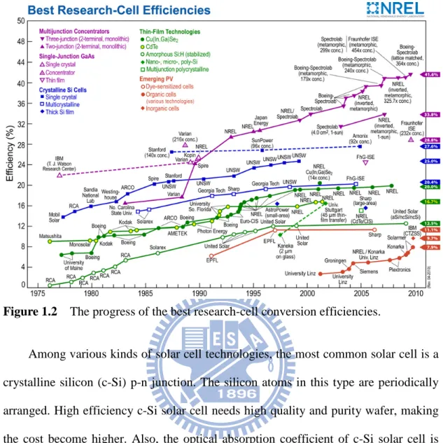
As shown in figure 2.1, the historical efficiency record released by Nation Renewable Energy Laboratory (NREL) demonstrates that the efficiency of the research-cell is still being improved in various kinds of solar cell. Generally speaking, the higher conversion efficiency often accompanies with higher cost or complicated fabrication process. The goal of grid-parity can only be achieved when the cost per watt is low enough compared to current fossil fuel.
3
Figure 1.2 The progress of the best research-cell conversion efficiencies.
Among various kinds of solar cell technologies, the most common solar cell is a crystalline silicon (c-Si) p-n junction. The silicon atoms in this type are periodically arranged. High efficiency c-Si solar cell needs high quality and purity wafer, making the cost become higher. Also, the optical absorption coefficient of c-Si solar cell is low since Si is in-direct band-gap material, which means the thickness should be thick to absorb enough photons. Once the price of c-Si rises, this high material consumption must increase the total cost of solar cell fabrication.
Compared to c-Si solar cell, thin film solar cell technology currently is developed to reduce the amount of light absorbing material. Also, it is carried out at lower temperature, making it possible to deposit on cheaper or flexible substrates such as glass or plastic substrate. In addition to low cost and flexibility, thin film solar cell technology has advantages including lighter weight and ease of integration compared to wafer silicon. Due the above benefits, thin film solar cell is promising in the energy field.
4
1.2.2 Thin Film Solar Cell Technology
There are several categories in thin film solar cell technology including Si thin film, Cadmium Telluride (CdTe), Copper Indium (Gallium) Selenide (CIS/CIGS), and Organic/polymer solar cell. The following are some introduction and characteristics about these thin film solar cells:
CdTe solar cell: With an optimal band-gap of 1.44 eV, CdTe is an efficient
light-absorbing material for thin film cells. The cell thickness only need to be around 1 μm, significantly reducing the material costs. Efficiencies close to 10% have been achieved in commercial modules by Solar Cells Inc. However, the toxicity of CdTe-based solar cell on health and the environment is still a concern.
CIS/CIGS solar cell: These semiconductors are attractive for their high optical
absorption coefficient and versatile optical and electrical characteristics can be manipulated to fit the needs for device. The best efficiency of CIGS solar cell has achieved 19.9% in 2008 [2]. By using optical concentrator or multi-junction tandem solar cell, higher efficiencies (>30%) can be obtained. But the manufacturing costs of CIGS solar cells are high when compared to amorphous silicon (a-Si) solar cells.
Organic/polymer solar cell: These devices don’t rely on built-in electric field
like inorganic solar cells. The active layer consists of two materials, one acts as an electron donor and the other as an acceptor. The efficiencies of organic/polymer solar cell has quickly improved in recent years and the best one has achieved 6.77% [3]. But the stability and excitation diffusion length should be enhanced in the future.
5
after oxygen, making up 25.7% of the crust by mass. That is the reason for hydrogenated amorphous silicon (a-Si:H) p-i-n solar cells is the most studied alternative energy method. Furthermore, the multi-junction technology can be also applied combining a-Si:H with hydrogenated microcrystalline silicon (μc-Si:H) solar cells. Triple stack a-Si:H/μc-Si:H/μc-Si:H achieved module efficiency up to 12% with much less photo-degradation [4]. Our group also focuses on this Si thin film solar cells.
1.2.3 Si Thin-Film Solar Cell
Si thin film solar cell consists of a-Si or μc-Si materials. Compared to c-Si solar cell, the light absorption coefficient of Si thin film solar cell is much higher, as shown in figure 1.3. Thus, the thickness (~1 μm) and Si material consumption can be effectively reduced, which can lower the solar cell cost.
6
Figure 1.3 Absorption coefficient α vs. energy for a-Si:H, μc-Si:H and crystalline
silicon[5].
1.3. Motivations
a-Si:H based thin-film solar cells are easier to large scale production and at low cost. a-Si:H solar cells can be deposited on flexible substrate, namely, a-Si:H solar cells can be a power source of 3C products.
However, the low conversion efficiency of a-Si:H solar cells is the main drawback. In this study we used Plasma Enhanced Chemical Vapor Deposition (PECVD) to fabricate a-Si:H solar cells. Several measures were taken to enhanced the conversion efficiency of a-Si:H solar cells.
7
Chapter 2
Literature Review
2.1. Introduction and Basic Theory of Solar Cells
In 1905, the photoelectric effect was explained by Elbert Einstein. The explanation relies on the ideas from quantum theory. Light is made up of a pack of photons, the photon energy depends only on the frequency (or wavelength) of light. When the wavelength of light is smaller than a threshold value (usually blue or ultraviolet light) then radiating on the surface of a metal, the electrons will absorb enough energy and escape completely. The escaping electrons are called photoelectrons. Because the work function of a metal is as high as 3 to 5 eV, so the maximum conversion efficiency of bounded electrons to photoelectrons is lower than 1%. This phenomenon is called as photoelectric effect and cannot be explained by wave theory, that is, the escape capability of bounded electrons depends on the energy of light, not on the intensity of light.
Generally speaking, the energy of photons in visible spectrum is sufficient to excite electrons to higher energy levels where they are easier to move, but the excited electrons will quickly relax back to their ground states.
In photovoltaic devices, there is a built-in electric field which can separate photo-generated carriers away and extract them to external circuit. The extra energy of excited electrons generates a potential difference which drives these electrons to external load and does electrical work. This phenomenon is the photovoltaic effect.
Figure 2.1 shows the simplified schematic diagram of a typical solar cell. The typical solar cell is a simple p-n junction device without applied voltage across the junction.
8
Figure 2.1 The principle of operation of the solar cell[6].
lp、ln: the width of p-region and n-region
Lh、Le: the minority carrier diffusion length to the depletion region W: the width of depletion region
Eo: the built-in field in the depletion region
Consider this p-n junction with thin and heavy-doped n-region, the illumination is through the n-region. The n-region is very narrow most of photons are absorbered in the depletion region and neutral p-region. The photo-generated holes in n-region and photo-generated electrons in p-region diffuse to the depletion region and these free carrier are immediately drifted by built-in field in the depletion region. The electrons drift and reach the neutral n-region that makes this region negative by an amount of charge –e. Similarly, holes drift and reach the neutral p-region that makes this region positive. If an external load is connected then the excess electrons in n-region can travel around the external circuit, reach to p-region to recombine with excess holes and do electric work.
9
2.2. Hydrogenated Amorphous Silicon (a-Si:H)
Figure 2.2a shows the structure of single crystal silicon schematically. Si is a four-fold coordinated atom that is normally tetrahedral bonded to four neighboring Si atoms. The unit cell and its duplicates next to each other, the regular atomic arrangement is described as a structure with long range order. Figure 2.2b illustrates that a-Si:H without long-range order. Though a-Si:H lacks of long range order, it has short ranger order same as single crystal silicon. Due to the short range order the concept of the energy bands, represented by the conduction and valence bands can be adapted to a-Si:H. Unlike single crystal Si epitaxial growth should be taken at high temperature around several hundred Celsius and grows on silicon wafer, the a-Si:H can be deposited at low temperature and on flexible or glass substrates. With this advantage a-Si:H is suitable option for roll to roll mass production. However, as shown in figure 2.2b the deviation in bond angles and bond lengths between a-Si bonds result in weak and strained bonds which are easier to be broken if they absorb enough energy, for example in the form of heat or radiation. The process is a leading cause of defect formation in the atomic network. Those defects in a-Si:H random network are noted as coordination defects [7]. That is the reason why a-Si is a defect-abundant material. The defect density of pure a-Si is about 1021 cm-3. Such material with so high defect density cannot be applied to electronic devices. a-Si can be deposited by PECVD from silane (SiH4). The hydrogen (H2) from SiH4 can be incorporated into amorphous silicon network and form stronger Si-H bonds. Therefore, in a-Si:H structure, the defect density decreases dramatically to 1015-1016 cm-3 due to dangling bond passivated by H2 radical. This material can be a candidate for electronic application.
10
Figure 2.2 Schematics representation of the atomic structure of (a) single crystal
silicon, (b) hydrogenated amorphous silicon [8].
Since the first report of depositing high quality hydrogenated amorphous silicon with hydrogen dilution [9] , the hydrogen dilution method is widely used to improve the quality of hydrogenated amorphous silicon. The mechanisms in hydrogen dilution silane plasma are concluded by S. Sriraman, et al [10]:
1. Hydrogen provides improved surface coverage that results in the impinging molecules diffusing further to find more favorable sites [11-12]
2. Hydrogen etches away the disordered regions, leaving behind the ordered structure [13-15]
3. Hydrogen atoms can be inserted into strained Si-Si bonds in the sub-surface region through the formation of a SiHn complex—structural relaxation (more ordered phase)[16-19]
Using hydrogen dilution can improve open-circuit-voltage (Voc) of solar cells due to the increase of hydrogen concentration in a-Si:H. The etching mechanism can remove the weak structure in a-Si:H bonding network and leave the solid structure, effectively enhancing the quality of a-Si:H film.
11
2.3. Doping of Hydrogenated Amorphous Silicon
Doping by thermal process is widely used for the doping of c-Si. Si wafers are put into the furnace and the dopants are introduced in the furnace at the same time. The dopants evaporate at such high temperature (900~950℃) and diffuse into silicon wafers. From W. Spear’s report[20], the conductivity of n and p-type a-Si:H as a function fraction of doping gases in the gas mixture with SiH4 is shown in figure 2.3.
Figure 2.3 Room temperature conductivity,σRT,of n and p-type a-Si:H plotted as a
function fraction of doping gases in the gas mixture with silane [20].
Unlike c-Sil, the chemical reaction in PECVD is a gas phase reaction, the doping of a-Si can be achieved by the introduction of doping source gases like B2H6、TMB、 PH3 as the deposition of a-Si in PECVD system.
12
2.4. Staebler-Wronski Effect
Electrical properties of a-Si would be changed under long time exposure to light. This phenomenon is well-known as Staebler-Wronski Effect discovered by D. L. Staebler and C. R. Wronski in 1977[21]. Weak bonds in a-Si like dihydride、trihydride bonds and cluster of Si-H may be broken and result in the formation of dangling bonds by long time illumination of light. When the defect density of dangling bonds increases, the lifetime of photo-generated carriers reduces. Due to the strong recombination loss through the localized states formed by the dangling bonds in a-Si network, the conversion efficiency degraded severely in a-Si:H based solar cells[22-23].
However, an essential feature of light-induced effects on a-Si:H film and solar cell can be recovered by annealing above 150℃. The performance of stabilized a-Si:H solar cells is 70 to 85% of their initial efficiency depends on the quality of a-Si:H film. This light-induced degradation is the major disadvantage of a-Si as a photovoltaic material.
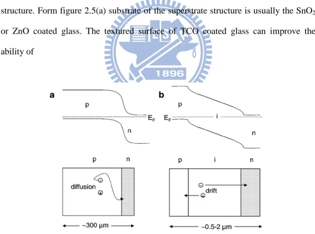
2.5. P-i-n Structure of Silicon Based Thin Film Solar Cells
There are three major mechanisms responsible to the collection of photo-generated carriers in p-n diode photovoltaic:
1. The drift current of holes and electrons in depletion region. 2. The diffusion current of minority carriers in n-type neutral region 3. The diffusion current of minority carriers in p-type neutral region
In typical mono-crystalline and poly-crystalline Si p-n diode photovoltaic, the contribution of photo-generated carriers in depletion region is trivial due to the width of this region is too thin compared to the diffusion length of minority carriers. The
13
main current of mono-crystalline and poly-crystalline solar cells is the diffusion current in the neutral region. The absorption coefficient of a-Si is about two orders higher than c-Si, the material needed in a-Si thin film solar cells is 1% of c-Si solar cells needed. However, a-Si is a defective material. The diffusion lengths are so short in doped a-Si, the undoped region is needed to extend the thickness which photons can be absorbed effectively. The thin p-layer and n-layer create the built-in field which drives the charges to separate. In the p-i-n structure photocarriers are collected primarily by drift rather than by diffusion. Figure 2.4 shows the band diagrams and sketches of p-n and p-i-n structures, respectively.
Figure 2.5 shows two typical configurations of a-Si:H solar cells with p-i-n structure. Form figure 2.5(a) substrate of the superstrate structure is usually the SnO2 or ZnO coated glass. The textured surface of TCO coated glass can improve the ability of
14
(a) (b)
Figure 2.5 (a) The superstrate cell configuration and (b) the substrate cell configuration.
light-trapping to the absorption of solar cells. From figure 2.5(b), the substrate of substrate structure can be flexible materials like stainless steel or plastic. Both configurations are usually illuminated through a TCO/p-layer interface. The short-wavelength light is mainly absorbed at the surface of solar cells, due to the short depth of penetration. The mobility of hole is much smaller than electron. For more efficient collection of photo-generated carriers and avoiding the recombination of holes, plane of incidence of light is usually p-layer which is also called as window layer in solar cells.
i-layer
n-type
Metal Electrode
p-type
TCO
Glass
L
L
i
i
g
g
h
h
t
t
i-layer
n-type
Metal Electrode
p-type
TCO
Substrate
L
L
i
i
g
g
h
h
t
t
15
2.6. Back Reflector
Back reflector is usually composed of a TCO layer and a metal layer like silver (Ag). The use of back reflector can enhance the absorption of light in the absorber layer especially in long-wavelength region. The Ag contact, with high reflectance, can serve as back reflector. However, the optical property of Ag back electrode next to n-type a-Si:H in superstrate structure is similar to that of Al [25] , indicating the reflection at the n-type a-Si:H/Ag interface is smaller to the expectation of bulk optical properties. The insertion of ZnO layer between n-layer and Ag significantly enhance the Jsc of solar cell by 15% to 20% compared to that without ZnO.[26]
2.7. Deposition Mechanism of PECVD
Many growth methods have been proposed to fabricate a-Si:H and μc-Si:H, e.g. hot-wire CVD, photo CVD, PECVD. Among these growth methods, plasma enhanced chemical vapor deposition (PECVD) system is widely used because its low substrate temperature during deposition (less than 300℃), good uniformity, and large scale productions.
PECVD is a deposition method where the reactive species are produced by an electrical discharge leading to plasma. The gas-phase reactions in glow discharges reduce the substrate temperature required for film deposition compared to thermal CVD, so various substrates can be used in this deposition process (like glass, stainless steel, or plastic substrate).
In order to yield a high quality Si thin film, electron impact dissociation of source gas, gas-phase reaction, radical diffusion and surface reaction have to be considered [27]. In this study, SiH4 and H2 are the source gas which is dissociated into reactive neutral and ions species by electron impact excitation in plasma. And these
16
reactive neutral and ions species have the secondary reactions with parent SiH4 and H2 molecules while they diffuse to the substrate [28] as shown in Table 2.1 . All the possible reactive neutral and ions species in plasma is given in [29]. Then, their reactive products interact with the surface of growing film, such as radical diffusion, chemical bonding, and hydrogen sticking to the growing film or re-emitted from the surface to gas phase.
Tab le 2.1 The Function of Primary Reactions and Secondary Reactions[29]
Primary reactions e + SiH4 → SiH2 + H2 + e SiH3 + H + e SiH + H2 + H + e SiH2 + H2 + 2e SiH3+ + H + 2e SiH3- + H Secondary reactions SiH4 + H → SiH3 +H2 SiH4 + SiH2→ Si2H6 SiH3 + SiH4→ SiH4 +SiH3
17
Chapter 3
Experimental Details
3.1. Experimental Introduction
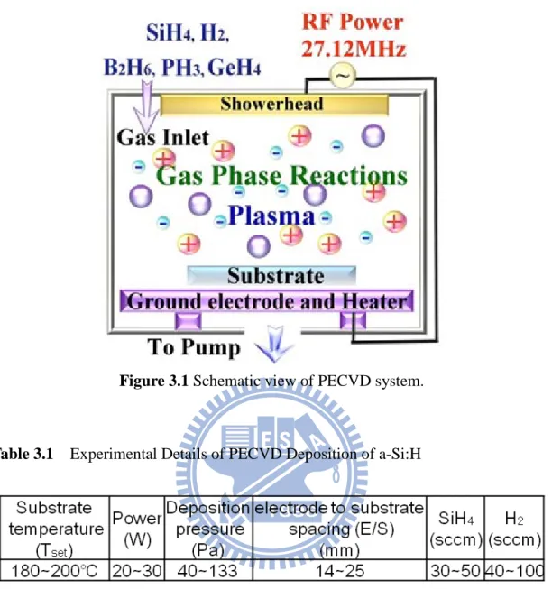
In this study, a-Si:H was prepared by radio frequency (27.12 MHz) plasma- enhanced chemical vapor deposition (PECVD) system. Substrates for a-Si:H single film are Corning Eagle 2000 glass and c-Si wafer which were cleaned by KG Cleaner diluted DI water and RCA standard cleaning process, respectively.
In figure 3.1, the substrate was transferred onto the heater. A showerhead electrode was used in this system, and source gas was fed in at the upper electrode. This electrode design improves the homogenous gas distribution and so does the uniformity of Si thin film. The area of the showerhead electrode is 26 x 26 cm2 and the volume of reaction chamber is 33.6 liter. All the samples were deposited until the background pressure reach to 5 x 10⁻⁴ Pa. Doping layers were prepared by using CH4, B2H6 or PH3 with SiH4 and H2. The complete range of a-Si:H deposition conditions was listed in table 3.1
In solar cell fabrication process, the reaction chamber is cleaned by Ar and NF3 plasma between intrinsic layer and doping layer to avoid cross contamination.
18
Figure 3.1 Schematic view of PECVD system.
Table 3.1 Experimental Details of PECVD Deposition of a-Si:H
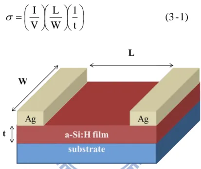
3.2. Photo Conductivity (σph) and Dark Conductivity (σd)
Photo conductivity (σph) and dark conductivity (σd) of intrinsic films were investigated by coplanar conductivity measurements at room temperature, and σph is measured under AM1.5 illumination. This is one way to obtain the information about material characteristic of a-Si:H. Besides, the photosensitive, σph / σd, is an useful parameter to determine the property of a-Si:H.[27]. The σd of a-Si:H used in devices should be lower than 10-10 (S/cm), and the σph should be higher than 10-5 (S/cm). Therefore, the σph / σd for a good quality a-Si:H thin film should be higher than 105.
19
In order to investigate the conductivity of the a-Si:H thin film, metal contacts were deposited onto the Si thin film by thermal evaporation. Conductivity is calculated by equation ( 3-1 ), where V and I are the bias voltage and measured current, respectively. The other relative parameters in equation ( 3-1 ) are shown in figure 3.2.
Figure 3.2 Schematics of the conductivity measurement.
3.3. Fourier Transform Infrared Spectroscopy (FTIR)
The incorporation of H2 in the a-Si is beneficial because of the defect passivation. Infrared absorption spectroscopy is widely used to investigate the Si-Hx bonding configurations [7]. A peak around 2000 cm-1 is defined as the stretching mode of the isolated Si-H bonds, and a peak around 2010 cm-1 is correlated with SiH2 and clustered (SiH2)n groups at internal surfaces of voids or grain boundries [30-31] . Different vibration frequencies for SiHx (x=1~3) in a-Si:H have been identified as shown in Table 3.2
1)
-(3
t
1
W
L
V
I
=
σ
20
The microstructure parameter (R) is defined as: R = I I2010
2000+ I2010
where I2000 and I2010 are the integrated absorption strength of the peaks at 2000 cm-1 and 2010 cm-1 respectively. The R ratio is widely used to characterize the microstructure in the a-Si:H network. As the 2100 cm-1 contribution increases, the ratio R increases which is the sign of poor quality material.
Tab le 3.2 Vibration frequencies of SiHx(x=1~3) in a-Si:H[32]
Group Stretching Bending Rocking / Wagging
SiH 2000 630
SiH2 2090 880 630
(SiH2)n 2090~2010 890,945 630
SiH3 2014 950,860 630
3.4. Determination of Optical Bandgap
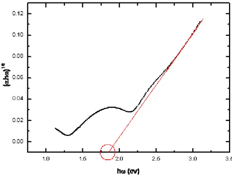
The optical bandgap of thin film use UV/VIS/NIR spectrometers to measure transmission (T) spectra were carried out between 200 nm and 1.3 μm in the step of 2 nm. Calculating optical bandgap (Eg) has to use transmission spectra and thickness of thin film in equation (3-2).
Figure 3.3 shows the photo energy ( ω) as function of the . The band gap value can be determined from the extrapolating of linear region to the intercept of a-axis.
(
αω)
12)
c
(
-
E
opt)
(3-2)
2 1ω
ω
α
=
(
21
Figure 3.3 Photon energy ( ω) as function of the and the Tauc band gap
value.
3.5. AM1.5 Light Source
The conversion efficiency of solar cells is closely related to the intensity and spectrum of incident solar radiation. However, as the sunlight travels though the atmosphere, chemicals react with the sunlight and absorb certain wavelengths. For the well-known example is the stripping of ultraviolet light by ozone in the upper atmosphere, which drastically reduces the amount of short wavelength light reaching the Earth's surface. Additionally, water vapor, nitrogen, oxygen and carbon dioxide in atmosphere results in a wide variety of absorption bands at many wavelengths
Generally, we use the air mass (A.M.) conception to define the absorption, scattering and reflection in the atmosphere and the location and angle of solar cells
Air mass= 1 / cos θ (3-3)
θ means the included angle between the incident angle of sunlight and ground.As
shown in figure 3.4, the spectrum outside the atmosphere, the 5,800 K black body, is
(
αω)
1222
referred to as "AM0", meaning "zero atmospheres". Cells used for space power applications, like those on communications satellites are generally characterized using AM0.
The spectrum after traveling through the atmosphere to sea level with the sun directly overhead is referred to as "AM1". This means "one atmosphere". Conveniently, Si solar cells are not very sensitive to the portions of the spectrum lost in the atmosphere. Since solar cell development is concentrated in the United States, Europe and Japan, an AM number representing the spectrum at mid-latitudes is much more common. "AM1.5", 1.5 atmosphere thicknesses, corresponds to a solar zenith angle of 48.2°, and is almost universally used to characterize solar panels.
Figure 3.4 Schematics of air mass.
3.6. Current-Voltage Characteristics of Solar cells
The measurement of I-V characteristics is the primary method to evaluate solar cells. It is measured under AM 1.5 light source.
23
• The efficiency (η) is defined as the ratio of the maximum power generated by the device and the radiation power incident in the area of cell.
• The short-circuit current density (Jsc)is the maximum current density generated by the device under light illumination.
• The open-circuit voltage (Voc) is the maximum voltage generated by the device under light illumination.
• The fill factor (F.F.) is defined as a ratio of maximum power generated by the cell and the ideal power generated which is equal to Isc× Voc. This factor relate to the shunt resistance, series resistance and material quality in the device.
24
Chapter 4
Results and Discussions
4.1. Effect of Methane to Silane Flow Rate Ratio on the Film
Property of p- type a-Si
Figure 4.1 illustrates the deposition rate of p-a-SiC:H as a function of CH4 to SiH4 flow rate ratio. Besides, the hydrogen to silane ratio was 2.5, the deposition pressure was controlled at 80 Pa. From figure 4.1, the deposition rate decreased with the increase of CH4 to SiH4 flow rate ratio. The main reason for this result can be attributed to the main source gas of p-type amorphous silicon carbide deposition. The reduced concentration of silane in plasma reasonably lowered the deposition rate.
1.0 1.5 2.0 0.00 0.05 0.10 0.15 0.20
D
e
pos
it
ion
ra
te
(nm
/s
)
CH
4/SiH
4Figure 4.1 The deposition rate of p-a-SiC:H as a function of CH4 to SiH4 flow rate ratio.
25 1.0 1.5 2.0 1E-7 1E-6 1E-5 1E-4
CH
4/SiH
4D
a
rk
C
o
n
d
u
c
ti
v
iy
(S
cm
-1 ) 1.9 2.0 2.1E
opt
(e
V)
Figure 4.2 The optical bandgap and dark conductivity of p-a-SiC:H as a function of
CH4 to SiH4 flow rate ratio.
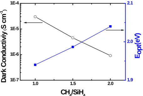
The optical bandgap and dark conductivity of p-a-SiC:H as a function of CH4 to SiH4 flow rate ratio can be observed figure 4.2. The optical bandgap apparently enlarged and dark conductivity drastically decreased with the increasing ratio of CH4 to SiH4.
More carbon was incorporated into amorphous silicon film with increasing the concentration of CH4 in source gases. The binding energy of Si-C is larger than Si-Si, consequently, the introduction of CH4 when depositing p-layer can enlarge the optical bandgap. However, the conductivity decreased as increasing the content of carbon in amorphous silicon network. P-type amorphous silicon carbide was served as a window layer and emitter layer in our cells. The values of electric conductivity and optical bandgap of p-layer should be a trade-off issue. The optical bandgap and dark conductivity should be larger than 2.0 e.V and 1*10-5S cm-1, respectively of optimal p-layer[27].
26
4.2. Effect of Electrode to Substrate Spacing on the Film
Property of Intrinsic a-Si
a-Si films were prepared with various electrode-to-substrate (E/S) distances. The distances were increased from 14 to 25 mm. The thickness of the films was fixed at around 400 nm. Deposition pressure and H2-to-SiH4 ratio for all samples were fixed at 1 torr and 2.5, respectively. The infrared transmission spectra of a-S:H films was plotted in figure 4.3. It can be seen in figure 4.4 that R decreases with the decrease of E/S spacing. When the E/S spacings were below 20 mm, only small variations of R were observed. When increasing the E/S spacing to 25mm, the R drastically increased to 0.285. This can be explained by the longer E/S spacing which induces more gas phase reaction. 1600 1800 2000 2200 2400 0.0 0.1 0.2 0.3 E/S:25mm E/S:20mm E/S:17mm
Int
e
ns
it
y
(
a
rb.
uni
ts
)
Wavenumber(cm
-1)
E/S:14mmFigure 4.3 Infrared transmission spectra of a-S:H films deposited at different E/S
spacing. .
These frequent collisions between reactive radicals when depositing a-Si:H film introduce the formation of the weak bonds like SiH2,(SiH2)n、SiH3. Those unstable
27
bonds may induce defects and micro-voids in a-Si:H network. The concentration of these bonds in high quality a-Si:H should be lower than 10% [27].
15 18 21 24 0.0 0.1 0.2 0.3
R
E/S distance (mm)
Figure 4.4 The microstructure parameter as a function of E/S spacing.
12 16 20 24 28 0.0 0.1 0.2 0.3 0.4
D
e
pos
it
ion
ra
te
(
nm
/s
)
E/S(mm)
Figure 4.5 The deposition rate as a function of E/S spacing.
The deposition rate with different electrode distance is shown in Figure 4.5. The deposition rate slightly increases with the increasing E/S distance. The relationship
28
between deposition rate and electrode distance can be attributed to more intense gas phase reaction[33] . The silane ionizes by non-elastic collision of high energy electron before arriving at the surface of substrate. Larger electrode distance enhances the probability of the ionization silane. The higher reactive radical concentration in plasma raises the deposition rate of a-Si:H thin flim.
15 18 21 24 1E-12 1E-11 1E-10 1E-9 1E-8 1E-7 1E-6 1E-5 1E-4
σ
d
σ
ph
C
onduc
ti
v
iy
(S
cm
-1)
E/S(mm)
Figure 4.6 The dependence of dark conductivity (σd) and photo conductivity (σph) on the E/S distance.
The open and closed symbols correspond to σph and σd, respectively. It can be seen in figure 4.6 that there is no significant difference in σdand σph with the increase of E/S distance. Therefore, the R in this region of 0 to 0.3 has no obvious influence on conductivity. This result is similar to the report by S. Okamoto, et al [34]. On the other hand, although the damage of the ion bombardment on a-Si:H films can be alleviated by applying larger electrode spacing, the deposition rate and microstructure parameter may more critically impact the performance of solar cells.
29
distances of 14, 20 and 25 mm were chose to deposit the intrinsic layer of the solar cell.
The solar cells have the following structure: glass/SnO2:F/p-type a-SiC:H/buffer layer /intrinsic a-Si:H (300nm)/n-type a-Si:H/Ag. The I-V curves of a-Si:H solar cells are shown in figure 4.7. We measured five devices on the same sample to verify the stability and repeatability. The performance of a-Si:H single junction solar cells versus different E/S spacing are plotted in figure 4.8. The solar cell deposited at E/S spacing of 14 mm has the best performance in this set of experiments, while others decrease their performance with increasing E/S spacing.
0 200 400 600 800 1000 0 2 4 6 8 10 12 14 16
C
u
rr
en
t D
en
si
ty
(mA
/c
m
2)
Voltage (mV)
E/S:14mm E/S:20mm E/S:25mmFigure 4.7 The I-V curve of a-Si:H single junction solar cells depositing at different
E/S spacing.
Figure 4.8 presents no significant variation in Voc and F.F. when altering the electrode spacing. The major improvement is the value of Jsc. This probably due to the
30
larger E/S distance leads to more collision between the radicals (ex:SiH3) ,which deposits defective intrinsic layer. Therefore, the photo-generated carriers quickly recombine before extracting from the absorber layer.
12 16 20 24 850 900 950 11 12 13 70 75 7.0 7.5 8.0 8.5 oc
E/S distance(mm)
V o c (mv ) J s c ( mA /c m 2 ) F F (% ) E ff ici ency (% )Figure 4.8 The device performance of a-Si:H single junction solar cells depositing
at E/S spacing.
4.3. Characterization of n-type a-Si Layer
The purpose of doping is to change electrical conductivity and its magnitude by adding a controlled amount of special impurity atoms. The principal doping elements used in a-Si:H are the same as in c-Si : boron (B) for p-type and phosphorus (P) for n-type material. We achieved a change in conductivity of a-Si:H the silicon source gas, SiH4, with PH3 during deposition using the glow discharge method [31]. The n-type
31
a-Si is mixing SiH4 and PH3 to change conductivity. Figure 4.9 shows the σd as function of SiH4 and PH3 flow rate ratio.
Figure 4.10 shows the band gap as function of PH3 to SiH4 ratio. The band gap and σd didn’t change too much. From figure 4.10, the trivial differences in σd of n-type a-Si can be attributed to the experimental deviation.
2 3 4 5 10-3 10-2 10-1
σ d
(S
cm
-1
)PH3/SiH4 ratio
(x10-3
)32 2 3 4 5 1.0 1.5 2.0 2.5
E
opt
(e
V)
PH3/SiH4 ratio
(x10-3
)Figure 4.10 The band gap as function of PH3 to SiH4 ratio.
4.4. Effect of the Addition of Back TCO on a-Si:H Solar
Cells
The addition of back TCO at the interface of n-type layer and Ag can surprising enhance the performance of a-Si:H p-i-n structure solar cells. The TCO we used is gallium-doped zinc oxide (GZO). Other substitutions could be zinc oxide (ZnO) or indium-doped tin oxide (ITO). The I-V curves of a-Si:H single junction solar cells with only Ag or TCO/Ag back contact are shown in figure 4.11. A significant improvement in Jsc can be observed from figure 4.11. Table 4.1 lists the performance of both cells. Compared to Ag, the introduction of higher resistant TCO leads to additional series resistance of solar cells. From Table 4.1, the slightly decrease in F.F. when applying TCO in solar cells could be attributed to the addition resistance.
33 0 200 400 600 800 1000 0 2 4 6 8 10 12 14 16
C
u
rr
en
t D
en
si
ty
(mA
/c
m
2)
Voltage (mV)
Ag onlyTCO/Ag back contact
Figure 4.11 The I-V curves of a-Si:H single junction solar cells with only Ag
contact and TCO/Ag back contact.
Tab le 4.1 Comparison of the Performance of a-Si:H Single Junction Solar Cells
between Ag only Contact and TCO/Ag Back Contact.
Because of the high optical reflectance of the combination of TCO/Ag, the optical path inside the solar cell was increased. The significant enhancement in Jsc results from the improved spectral response at the long wavelength range(~600 nm) [35].Although the F.F. slightly decreased from 74.88% to 72.98%, the Jsc significantly improved from 12.38 mA/cm2 to 13.94 mA/cm2 with the application of TCO/Ag back
34
contact. As a result, the efficiency significantly improved from 8.39% to 9.23%.
4.5. Effect of p, b, i, n Thickness on the Performance of the
a-Si:H Solar Cells
4.5.1. Effect of p-layer Thickness on the Performance of a-Si:H Solar
Cells
In a-Si:H solar cells, the p-layer not only establishes the built-in field but also served as a window layer. Concerning wide bandgap and high conductivity of p-layer, we chose B-doped a-SiC as the p-layer for photovoltaic device. The p-type a-SiC layer was deposited with a mixture of SiH4, CH4, H2, %and B2H6 by PECVD. The substrate temperature of the devices was set at 190℃. The deposition pressure of n-type layer was 80 Pa and hydrogen dilution ratio was 2.5. The flow rate ratio of 2% B2H6 in H2 to SiH4 was 0.125 and the flow rate ratio of CH4 to SiH4 was 1.25. The thicknesses of the p-layers were in the range of 5 to 12nm.
The optical bandgap calculated from the measured Tauc’s plot is 1.94 eV and the σd is around 1.2x 10⁻⁵S/cm. The structure of the solar cells is illustrated in figure 2.5(b), the back contact of cells are TCO/Ag. The illuminated area of the solar cell was defined by the Ag pattern. The resulting I-V curves of solar cells are shown in figure 4.12. It can be seen from figure 4.13 that the Voc seems to be saturated when the thickness of p-layer is above 8nm. The Jsc increases when the thickness increases from 5 to 8 nm, however, a drop was observed as the thickness increases to 12 nm. The change of p-layer thickness in this range has no significant influence on F.F.
35 0 200 400 600 800 1000 0 2 4 6 8 10 12 14 16 18 p-layer thickness: 8nm
C
u
rr
en
t D
en
si
ty
(mA
/c
m
2)
Voltage (mV)
p-layer thickness: 5nm p-layer thickness: 12nmFigure 4.12 The I-V curves of a-Si:H single junction solar cells with different
p-layer thicknesses.
Table 4.2 The Performance of Solar Cells with Different p-layer Thicknesses.
The results shown in figure 4.13 suggest a optimal thickness of p-layer around 8 nm. Too thin the p-layer may not be able to cover all the surface of SnO2:F, resulting in lack of build-in field microscopically. As a result, the generated current cannot be extracted and the Jsc decreased. Additionally, the SnO2:F coated glass substrate we applied is a kind of degenerate n-type transparent conductive oxide (TCO) [36]. To compensate the electron carrier at the front TCO/p and p/i interface, sufficient holes
36
quantity is required. Too thin the p-layer forms incomplete depletion region, resulting in the decrease of magnitude of the built-in potential in the intrinsic layer which weakens the ability of photo-generated current collection. Furthermore, the contact barrier height caused by TCO/p heterojunction influences the value of built-in voltage of devices. The Voc seems to saturate as the p-layer thickness increases. This result can be attributed to the sufficiently thick p layers, the TCO front contact is largely screened from the rest of the device [37-38]; hence, built-in voltage is mainly determined by the p layer properties and the contact barrier height has a smaller effect. The saturation happens with p-layer thicker than 10 nm were also presented in J. Arch’s report [37].
The above assumption can be verified from the degradation in Voc and Jsc in figure 4.13. However, p-layer is served as a window layer in this structure. The optical absorption in p-layer should be controlled as low as possible. It can be seen in figure 4.13 that the Jsc reduces sharply as the p-layer thickness increase to 12nm. This result can be concluded that the redundant p-layer either absorbs incident light or leads to a strong recombination of photo-generated carriers.
37 4 6 8 10 12 800 850 900 950 13 14 15 70 75 80 8.0 8.5 9.0 9.5 10.0 V o c (mv ) Thickiness of p layer (nm) Jsc ( mA /c m 2 ) FF ( % ) E ff ici en cy (% )
Figure 4.13 The performance of a-Si:H single junction solar cells as a function of
p-layer thickness.
4.5.2. Effect of Buffer Layer Thickness on a-Si:H Solar Cells
The bandgap of the p-type layer is around 2 eV while the bandgap of the intrinsic a-Si:H is about 1.75eV. The band offsets between the energy bands forms a heterojunction at p/i interface. A well-known solution to overcome the carrier transportation barrier is the addition of a buffer layer between the p-type layer and the intrinsic layer. The application of buffer layer can improve the conversion efficiency of a-Si:H solar cell. To investigate the effect of buffer layer thickness on the performance of a-Si:H photovoltaic device, three solar cells with different buffer layer thickness were fabricated to investigate this issue. The deposition pressure of the buffer layer was 60 Pa and H2 to SiH4 ratio was 2.5. The flow rate ratio of CH4 to SiH4 was 1. Devices were prepared at 190℃. The buffer layer thickness was 5、10、
38
15nm, respectively. The gases for the deposition of buffer layer (a-SiC) were SiH4, CH4 and H2. The p-type layer, intrinsic layer and n-type layer were fixed at 8 nm、300 nm、30 nm, respectively. No TCO/Ag back reflector was applied in the structure of solar cells in this section. The I-V curves and performance of a-Si:H single junction solar cells with different buffer layer thickness were shown in figure 4.14. and figure 4.15, respectively. From figure 4.14, the value of Voc slightly enhanced from 887 mV to 913 mV when enlarging the buffer layer thickness from 5 to 15 nm. When the buffer layer thickness exceeded 10 nm, the F.F. dropped to 69.59%.
0 200 400 600 800 1000 0 2 4 6 8 10 12 14 16 10 nm 15 nm 5 nm
C
u
rr
en
t D
en
si
ty
(mA
/c
m
2)
Voltage (mV)
Figure 4.14 The I-V curve of a-Si:H single junction solar cells with different buffer
layer thickness.
In addition to improve the bandgap differences of the p/i interface, a buffer layer can also be served as a film to prevent B diffusion from p-layer. The optimal thickness of buffer layer in our devices was around 10 nm. From figure 4.15, the enhancement in Voc as a function of buffer layer thickness may be ascribed to the contribution of
39
wide bandgap of intrinsic SiC. Since the conductivity of intrinsic SiC is low, too thick the buffer layer leads to the addition of series resistance in photovoltaic device.
5 10 15 880 900 920 11 12 13 65 70 75 7.5 8.0 8.5 Voc [mV ]
Thickiness of buffer layer (nm)
Jsc [ mA /c m 2 ] F F [% ] E ff ici en cy [% ]
Figure 4.15 The performance of a-Si:H single junction solar cells as a function of
buffer layer thickness.
4.5.3. Effect of i-layer Thickness on a-Si:H Solar Cells
The thickness of the intrinsic layer is a trade-off between optical absorption and photo-generated carriers collection. The thicker the intrinsic layer, the higher the absorption. However, the collection of photo current is more efficient in thinner layer. The current transportation mechainsm in a-Si:H thin film solar cell is mainly the drift current. The built-in potential across the device is determind by the Fermi level position of the doped layer and the i-layer thickness. Moreover, thicker absorber layer
40
may reach higher initial efficiency, but the stable conversion efficiency may be sharply deteriorated due to the Stabler Wronski effect . To verify the optimal thickness of intrinsic layer, experiments of the performance of solar cells as a function of intrinsic layer thickness was conducted. The intrinsic layer was deposited with SiH4 and H2 by PECVD. The flow rate of SiH4 was set from 30 to 60 sccm, the H2 dilurion ratio (H2/ SiH4) was fixed at 2.5. All devices were prepared at a pressure of 1 torr and temperaure of 190℃. The thickness of the intrinsic layers were varied from 250 nm to 600 nm.
Figures 4.16 and 4.17 illustrate the I-V curves and the performance of a-Si:H solar cells as a function of intrinsic layer thickness. According to figures 4.16 and 4.17, the highest open circuit voltage can be obtained as the intrinsic thickness is 250 nm. Because the photons in the long wavelength region are totally absorbed by thick intrinsic layer, the Jsc increases with the increasing intrinsic layer. The scattered results of 300 nm and 400 nm i-layer should be the cause of experimental error.
The F.F. degraded with the increase of intrinsic layer thickness. As mentioned in previous paragraph, too thick the i-layer deteriorates the electric field which leads to the weak collection of photocurrent. The record conversion efficiency of 9.45% was achieved as the i-layer exceeded 300 nm. The Jsc increased from 12.9 mA/cm2 to 15.17 mA/cm2as the thickness of the intrinsic layer increased from 250 nm to 600 nm. The improvement in Jsc should be due to the further absorption in a thicker layer.
41 0 200 400 600 800 1000 0 2 4 6 8 10 12 14 16 250 nm 400 nm 300 nm
C
u
rr
en
t D
en
si
ty
(mA
/c
m
2)
Voltage (mV)
600 nmFigure 4.16 The I-V curves of a-Si:H single junction solar cells with different
intrinsic layer thickness.
Tab le 4.3 The Performance of a-Si:H Single Junction Solar Cells as a Function of
42 200 300 400 500 600 880 900 920 13 14 15 16 68 70 72 74 8.5 9.0 9.5 V oc (mV ) Thickiness of i layer (nm) J sc ( mA /c m 2 ) F F (% ) E ff ici ency (% )
Figure 4.17 The performance of a-Si:H single junction solar cells as a function of
intrinsic layer thickness.
4.5.4. Effect of n-layer Thickness on a-Si:H Solar Cells
The deposition pressure of n-type layer was 60 Pa and H2 to SiH4 ratio was 2. The flow rate ratio of 1%PH3 in H2 to SiH4 was0.25. Devices were prepared at 190℃. Figures 4.18 and 4.19 illustrates the I-V curves and the performance of a-Si:H solar cells as a function of n-type layer thickness. There is no significant difference observed as the n-type layer thickness increased from 20 nm to 30 nm. However, poor performance of solar cell appeared as the n-type thickness decreased to 15 nm. The Voc, F.F. and conversion efficiency drastically decreased. One possible reason for this result can be ascribed to the lack of surface coverage on the i-layer which is similar to the effect of p-layer thickness in the previous section.
43 0 200 400 600 800 1000 0 5 10 15 15 nm 20 nm 30 nm
C
u
rr
en
t D
en
si
ty
(mA
/c
m
2)
Voltage (mV)
Figure 4.18 The I-V curves of a-Si:H single junction solar cells with different
n-type layer thicknesses.
15 20 25 30 860 880 900 920 13 14 15 65 70 75 8 9 10 Voc (mV ) Thickiness of n layer (nm) Jsc ( mA /c m 2 ) F F (% ) E ff ici en cy (% )
Figure 4.19 The performance of a-Si:H single junction solar cells as a function of
44
4.6. Effect of Bandgap Grading at p/i Interface on a-Si:H Solar Cells
The band offset caused by the heterojunction between p-type SiC window layer and a-Si absorber layer induces defect at p/i interface. This defective heterojunction acts as a recombination center which limits the performance of a-Si:H solar cells due to recombination losses [39-40]. In conventional p-i-n structure, the presence of large defect densities at the interfaces results in a strong electric field at this region [41]. The electric filed is relatively low in the i-layer. Although the introduction of wide bandgap buffer layer at the p/i interface can obtain high initial conversion efficiency, the stable efficiency degrades sharply after long time exposure of light [40, 42-44].
One solution to this inevitable problem was inserting a SiC between p-i layers as a buffer layer with bandgap engineering. In this experiment we altered the flow rate of CH4 to manipulate the bandgap of buffer layer. The intrinsic layer thickness of both devices was fixed at 300nm. The doped layers in a-Si:H solar cells were deposited under the same condition as mentioned in the previous section. No addition of back TCO was applied in the p-i-n structure a-Si:H solar cells.
Figure 4.20 illustrates the optical bandgap and photoconductivity of a-SiC as a function of CH4 to SiH4 flow rate ratio. The optical bandgap increased with increasing CH4 to SiH4 flow ratio due to the higher carbon concentration in the film. On the contrary, the photo conductivity decreased with CH4 to SiH4 flow ratio attributed to the increase defect density induced by the incorporation of carbon into amorphous silicon network.
45 0.0 0.5 1.0 1.5 1E-9 1E-8 1E-7 1E-6 1E-5
CH
4/SiH
4P
h
o
to
C
o
n
d
u
c
ti
v
iy
(S
cm
-1 ) 1.6 1.8 2.0 2.2E
opt
(e
V)
Figure 4.20 The optical bandgap and photo conductivity of a-SiC:H as a function of
CH4 to SiH4 flow rate ratio.
0 200 400 600 800 1000 0 2 4 6 8 10 12 14 16
C
u
rr
en
t D
en
si
ty
(mA
/c
m
2)
Voltage (mV)
conventional buffer layer bandgap profiling buffer layerFigure 4.21 The I-V curves of a-Si:H single junction solar cells between
conventional and grading buffer layer.
Figure 4.21 illustrates the I-V curves of both cells with conventional and grading buffer layer. The significant increase in Jsc can be observed from figure 4.21. Table 4.4
46
lists the performance parameters of both cells. The application of bandgap graded buffer layer in solar cells improved the Jsc from 11.84 mA/cm2 to 12.44 mA/cm2 and enhanced conversion efficiency from 7.95% to 8.31%, compared to the use of conventional buffer layer.
Tab le 4.4 The Performance of a-Si:H Single Junction Solar Cells between
Conventional and Graded Buffer Layer.
The value of Voc and F.F. didn’t deviate obviously with the addition of the graded buffer layer. The improvement in the performance of the solar cells is the contribution of the decreasing interface state with the incorporation of bandgap profiling at the p/i interface.
4.7. Effect of Hydrogen Plasma Treatment at Interface on a-Si:H
Solar Cells
During the fabrication of our cells, the robot arm took the sample away from the PECVD chamber after the deposition of the p-layer. An in-situ cleaning was carried out to prevent the boron contamination when depositing the next layer. We applied H2 plasma treatment between the cleaning process and the next layer deposition. To verify the etching effect and chemical annealing of H2 plasma on the performance of a-Si:H thin solar cells, H2 plasma treatment at the interface of each layer of solar cells
47
was employed. The H2 flow rate was 270 sccm, the processing pressure was controlled at 200 Pa and the input power was 200 W. The treatment time at each interface was 5 sec. The solar cells were prepared at the optimum condition concluded in previous sections. The thickness of main absorber layer was controlled at around 300nm.
Figure 4.22 illustrates the I-V curves of a-Si:H single junction solar cells with H2 plasma treatment at different interface. The square symbol represents the baseline cell without any treatment which shows the lowest Jsc. The first H2 plasma treatment was applied at p/b interface, The Jsc significantly improved from 13.30 mA/cm2 to 14.02 mA/cm2 and the conversion efficiency from 8.87% to 9.33%. The impurity such as water vapor、oxygen、organic gas may incorporate onto the surface of p-type layer. The p/i interface is one of the most critical spots that influence the performance of p-i-n solar cell greatly. The etching from H2 plasma can remove those impurities, providing a new and clean surface for the next layer deposition. Furthermore, the H2 plasma can passivate dangling bonds, and reduce the p/i interface induced defects.
![Figure 1.1 The change in the global energy composition until 2050/2100 [1].](https://thumb-ap.123doks.com/thumbv2/9libinfo/8761418.208277/12.892.155.742.776.1080/figure-change-global-energy-composition.webp)
![Figure 1.3 Absorption coefficient α vs. energy for a-Si:H, μc-Si:H and crystalline silicon[5]](https://thumb-ap.123doks.com/thumbv2/9libinfo/8761418.208277/17.892.138.725.121.739/figure-absorption-coefficient-energy-μc-and-crystalline-silicon.webp)
![Figure 2.3 Room temperature conductivity,σ RT ,of n and p-type a-Si:H plotted as a function fraction of doping gases in the gas mixture with silane [20]](https://thumb-ap.123doks.com/thumbv2/9libinfo/8761418.208277/22.892.258.670.416.844/figure-temperature-conductivity-plotted-function-fraction-mixture-silane.webp)