ECS Solid State Letters, 2 (2) P15-P18 (2013) P15 2162-8742/2013/2(2)/P15/4/$28.00©The Electrochemical Society
Concentration Gradient of Ni in Reduced SnAg Thickness
in Ni/SnAg/Cu Microbumps during Solid-State Aging
Tao-Chi Liu, Yi-Sa Huang, and Chih Chenz
Department of Materials Science & Engineering, National Chiao Tung University, Hsin-chu 30010, Taiwan We investigate the cross-interaction in Cu/SnAg/Ni microbumps with a reduced solder thickness of 30 and 10μm. The concentration of Ni atoms at the opposite site increased with the decrease in solder-height. A considerable concentration gradient of Ni was detected in 10-μm microbumps sample, which strongly triggers the diffusion of Ni atoms to the Cu side. The diffused Ni atoms at Cu side form the ternary intermetallic compounds of (Cu,Ni)6Sn5, which possesses a lower free energy than Cu6Sn5does. Eventually, the growth of the Cu3Sn was inhibited due to the formation of the thermodynamically stable (Cu,Ni)6Sn5.
© 2012 The Electrochemical Society. [DOI:10.1149/2.009302ssl] All rights reserved.
Manuscript submitted July 16, 2012; revised manuscript received November 7, 2012. Published November 28, 2012.
Three-dimension (3D) integrated circuits (ICs) packaging offers a high system integration by connecting multiple ICs chips which have different functions. To minimize the vertical packaging size, microbumps are adopted for connecting the I/O pads on between chips.1–4The bump height of the microbump is typical between 5 to 20μm and the solder volume is smaller than traditional solder bumps. The distance between the two metallization pads across the solder is very close as well.
During the reflow processes, solder reacts with the metallization materials, to form the intermetallic compounds (IMCs). Two chips are joined together through the IMCs in the microbumps. When two different metallization materials are adopted across the solder joints, interdiffusion can occur inside the solder joints during reflow process or solid-state aging.5–7 For example, it is quite common that Cu is adopted as one of the metallization material, and Ni serves the other one on the opposite side. Cu atoms may diffuse to the Ni side to affect the growth of the interfacial IMCs. Ni atoms can also migrate to the Cu end to influence the IMCs there.8–12Furthermore, the minor species in solder can also affect the growth of interfacial IMCs.13–21 For instance, a small amount of Ni in solder is able to influence the growth of microstructure in the Cu6Sn5IMCs.22–25It is reported that the addition of Ni atoms will ease the formation of Cu3Sn.26,27
During solid-state aging, Chang et al.9found that the atomic flux of Ni is about 25-40 times lower than that of Cu in ball grid array (BGA) and flip chip packaging. Nevertheless, Ni atoms still diffused through 400μm solder and affected the interfacial reaction on the other side after several hundred hours of thermal aging. As the bump height continuous to shrink in 3D IC packaging, the interdiffusion between the two metallization materials become more significant, but only few studies discussed the issue. Huang et al.28reported a Ni concentra-tion gradient in reflowed microbumps dominated the IMCs thickness during reflow process. However, whether there exists a Ni concentra-tion gradient during solid-state aging and the Ni distribuconcentra-tion in the Cu-Ni-Sn ternary IMCs are not clear. However, the concentration of Ni across the low-bump-height solder joint and its effect on the IMCs growth have not been reported. In this study, we investigate the cross-interaction across the solder joints with two different bump heights. A detailed focused ion beam (FIB) study including cross-sectional polishing and morphologies observation of (Cu,Ni)6Sn5 and Cu3Sn IMCs has been performed. Compositional analysis by electron probe X-ray microanalyzer (EPMA) was performed to map the distribution of Cu and Ni atoms in the microbumps.
Experimental
To prepare the microbumps, materials for under bump metallurgy (UBM) were firstly deposited on a Si substrate by electroplating a metal layer of 3-μm Ni or 10-μm Cu, and then followed by the elec-troplating of Sn2.3Ag lead-free solder on the Ni or Cu UBM. A chip
zE-mail:[email protected]
with Cu/Sn2.3Ag microbumps was flipped over and joined to an-other chip with Ni/Sn2.3Ag microbumps at 260◦C for 3 min on a hot plate. Thus, Cu/Sn2.3Ag/Ni sandwich samples can be fabricated. Sim-ilarly, controlled samples of Cu/Sn2.3Ag/Cu structure were prepared by bonding two chips with Cu/Sn microbumps. The solder height was controlled to a thickness of approximately 10μm and 30 μm in the bonded microbumps. Then solid-state aging was performed at 150◦C for 0, 100, 500 and 1000 h in a nitrogen-filled oven. To clearly observe the morphologies of IMCs, the aged samples were cross-sectioned and were polished utilizing a dual-beam FIB. The details for the polishing procedure is reported in our previous publication.29 Therefore, the microstructure of the thin Cu3Sn and (Cu,Ni)6Sn5can be observed without suffering mechanical destruction. Elemental dis-tributions were analyzed by FE-EPMA (JXA-8800M, JEOL).
Results and Discussion
With the FIB polishing, different layers exhibit clear contrasts in FIB images, as shown in Figures1. Figure1ashows the cross-sectional FIB image for an as-fabricated microbump. The (Cu,Ni)6Sn5IMCs form in both the solder/Ni and solder/Cu interfaces with 10-μm-thick solder. The IMCs 10-μm-thickness on the Cu side was 10-μm-thicker than that on the Ni side, which has been reported by Huang et al.28A thin Cu3Sn layer formed between the (Cu,Ni)6Sn5and Cu UBM, as labeled in the Figure. Compositional analysis by EPMA indicates that the Ni concentration is 0.7 at.% in the solder close to the (Cu,Ni)6Sn5 IMC on the Cu side. Yet, it is 1.3 at.% in the solder near to the
Figure 1. Cross-sectional FIB image for (a) the as-fabricated Cu/Sn2.3Ag/Ni microbump reflowed at 240◦C after 3 min; and solid-state aged at 150◦C for (b)100 h; (c) 500 h; (d) 1000 h.
) unless CC License in place (see abstract).
ecsdl.org/site/terms_use
address. Redistribution subject to ECS terms of use (see
140.113.38.11
P16 ECS Solid State Letters, 2 (2) P15-P18 (2013)
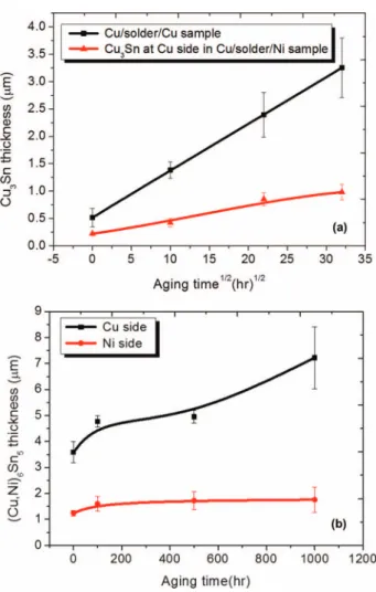
Figure 2. (a) The measured thickness of Cu3Sn IMCs at 150◦C against the square root of the aging time for Cu/Sn2.3Ag/Ni and Cu/Sn2.3Ag/Cu mi-crobumps. (b) The average thickness of (Cu, Ni)6Sn5on the Cu and Ni sides as a function of the aging time for Cu/Sn2.3Ag/Ni microbumps.
(Cu,Ni)6Sn5IMCs on the Ni side. Thus, there exists a Ni concentration gradient across the solder joint during solids-state aging at 150◦C, which provides the driving force for the Ni to diffuse to the Cu side. In addition, it is reported that the formation of ternary Cu-Ni-Sn IMCs will lower the free energy of the system.30,31Thus, the change of the free energy also drives the diffusion of the Ni atoms to the Cu side.
The Ni UBM can effectively inhibit the growth of the Cu3Sn IMCs at the Cu side. Figure1bto1dpresent the cross-sectional FIB images for the Cu/Sn2.3Ag/Ni sample after aging at 150◦C for 100,500, and 1000 h, respectively. The IMCs on the both interfaces grew thicker when the aging time increased. In particular, the (Cu,Ni)6Sn5 IMCs on the Cu side grew from 3.8μm to 7.2 μm after the aging for 1000 h. However, it is interesting that the Cu3Sn layer did not grow much. The thickness of the Cu3Sn was only 1.0μm after 1000 h aging. For comparison, the controlled sample of Cu/Sn2.3Ag/Cu was also aged at 150◦C for 1000 h. Figure2ashows the measured Cu3Sn thickness as the square root of the aging time for both samples. It is apparent that the Cu3Sn IMCs in the Cu/Sn2.3Ag/Cu grew faster than that in the Cu side of the Cu/Sn2.3Ag/Ni sample. The Cu3Sn layer can grow to 3.2μm after aging for 1000 h in Cu/SnAg/Cu sample. Figure2b illustrates the thickness of (Cu,Ni)6Sn5 IMCs against the aging time in the Cu/Sn2.3Ag/Ni sample. The IMCs on the Cu side grew much faster than that on the Ni side. Yet, the Cu3Sn layer grew to only 1.0μm after 1000 h aging. Therefore, it is evident that the Ni UBM can ease the growth of the Cu3Sn layer on the Cu side, although the (Cu,Ni)6Sn5on the Cu side has grown to 7.2μm.
Figure 3. EPMA color mapping of Cu/Sn2.3Ag/Ni microbumps aged at 150◦C showing Ni distributions for (a) 0 h; (b) 100 h; (c)500 h and (d) 1000 h.
To examine how the Ni atoms can ease the growth of the Cu3Sn, elemental mapping of Cu and Ni atoms was carried out by EPMA. Figure3athrough3dshows the evolution of Ni distributions in the microbumps after aging for 0, 100, 500, and 1000 h. In addition, quantitative analysis was also performed to measure the concentration of Cu, Ni, Ag and Sn in the samples at various locations. TableIlists the measured concentrations for the four elements. The results show that Ni atoms diffused to the Cu side to form (Cu,Ni)6Sn5 IMCs. The Ni atoms dissolved in the IMCs relatively uniformly. In addition, as the aging time increased, not only the IMCs on Cu side became thicker, but also the Ni concentration in the IMCs increased. The Ni concentration was 2.0 at.% in the (Cu,Ni)6Sn5close to the solder. It increased to 2.4 at.% after the aging for 500 h and 1000 h. The trend behaves the same in the (Cu,Ni)6Sn5IMCs close to the Cu3Sn layer. Therefore, a lot of Ni atoms diffused to the Cu side during the solid state aging. The formation of the (Cu,Ni)6Sn5 IMCs may inhibit the growth of Cu3Sn layer on the Cu side due to the (Cu,Ni)6Sn5IMCs possess a lower free energy than Cu6Sn5does.28,29During solid-state aging, Cu3Sn IMCs grows at the expense of Cu6Sn5.32 Therefore, the Cu3Sn layer grow slowly when the Cu6Sn5IMCs transform into (Cu,Ni)6Sn5IMCs, which has a lower free energy than Cu6Sn5.
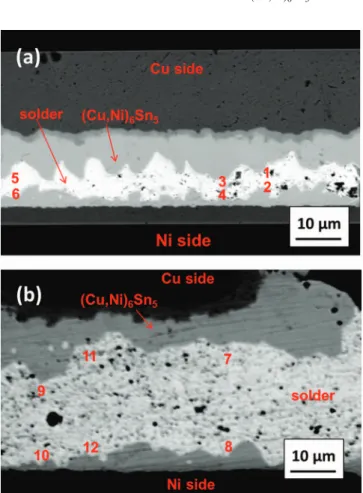
The EPMA results indicate that a Ni concentration gradient across the solder joints is increased with the decrease in solder-height. Figure4aand4bshow the cross-sectional SEM image of the 10-μm and 30-μm solder, respectively. The numbers labeled on the figures represent the locations for EPMA compositional analysis. Table II lists the Ni concentrations of the three locations and the correspond-ing concentration gradient of Ni across the solder joint. The average Ni concentration is 2.3± 0.3 at.% and 0.9 ± 0.2 at.% in (Cu,Ni)6Sn5 IMCs on the Cu side of the 10-μm and 30-μm solder, respectively. Furthermore, in 10-μm solder sample, both the concentration of Ni in solder and the concentration gradient of Ni are higher than those in the 30-μm solder sample. For 30-μm solder sample, the Cu side (Cu,Ni)6Sn5 IMCs and Cu3Sn grew to 7.4μm and 2.8 μm, respec-tively. It is evident that the Ni flux to the Cu side in the 10-μm solder sample is higher than that in the 30-μm solder sample, which may be mainly attributed to the higher Ni concentration gradient in the 10-μm solder sample. As mention earlier, the thickness of Cu3Sn IMCs in 10-μm solder sample is only 1.0 μm. The higher Ni flux eliminates the Cu3Sn effectively.
) unless CC License in place (see abstract).
ecsdl.org/site/terms_use
address. Redistribution subject to ECS terms of use (see
140.113.38.11
ECS Solid State Letters, 2 (2) P15-P18 (2013) P17
Table I. Result of compositional analysis by EPMA (beam size 0.5μm) at different locations in the Cu/Sn2.3Ag/Ni microbumps. Atomic percentage (%)
Aging Point Location Sn Ag Cu Ni
0 h 1 (Cu,Ni)6Sn5close to Cu3Sn on Cu side 25.0 < 0.1 74.5 0.4
2 (Cu,Ni)6Sn5close to solder on Cu side 44.5 0.2 53.3 2.0
3 Solder near Cu side 95.5 < 0.1 3.8 0.7
4 Solder near Ni side 95.7 < 0.1 2.9 1.3
5 (Cu,Ni)6Sn5at Ni side 45.0 0.1 50.6 4.3
500 h 6 (Cu,Ni)6Sn5close to Cu3Sn on Cu side 25.0 < 0.1 74.4 0.6
7 (Cu,Ni)6Sn5close to solder on Cu side 46.8 < 0.1 50.7 2.4
8 Solder near Cu side 96.2 < 0.1 3.2 0.6
9 Solder near Ni side 95.5 < 0.1 2.4 2.1
10 (Cu,Ni)6Sn5at Ni side 45.1 < 0.1 30.5 24.4
1000 h 11 (Cu,Ni)6Sn5close to Cu3Sn on Cu side 26.2 < 0.1 72.6 1.1
12 (Cu,Ni)6Sn5close to solder on Cu side 45.8 < 0.1 51.6 2.4
13 Solder near Cu side 95.8 < 0.1 3.8 0.5
14 Solder near Ni side 95.8 < 0.1 2.6 1.7
15 (Cu,Ni)6Sn5at Ni side 40.8 < 0.1 26.9 32.3
Figure 4. Cross-sectional SEM image showing the locations of EPMA quan-titative analysis for the Cu/Sn2.3Ag/Ni microbumps with a bump-height of (a) 10μm and (b) 30 μm, aged at 150◦C for 1000 h.
Conclusions
In summary, we have examined the cross-interactions in the Ni/ Sn2.3Ag/Cu in the 10-μm and 30-μm solder-height microbumps. When the solder-height reduce to 10 μm, it is found that the (Cu,Ni)6Sn5IMCs on the Ni side grew slowly during solid state aging at 150◦C. However, the (Cu,Ni)6Sn5IMCs on the Cu side grew faster than those on the Ni side. The formation of the ternary (Cu,Ni)6Sn5 on the Cu side suppress the growth of Cu3Sn IMCs due to the lower free energy of the ternary IMCs. EPMA quantitative analysis
demon-Table II. Result of compositional analysis by EPMA at different locations in the Cu/Sn2.3Ag/Ni microbumps in Figure4.
Bump Ni Solder length between Concentration gradient
height Point at.% the measured points(μm) (at.% perμm)
1 0.3 5.1 0.24 2 1.5 3 0.5 2.9 0.31 10μm 4 1.4 5 0.9 10.0 0.04 6 1.3 7 0.7 27.8 0.01 8 0.9 30μm 9 0.8 17.8 0.01 10 0.7 11 0.8 24.4 0.00 12 0.7
strated that the Ni concentration gradient of the microbumps plays an important role to the Ni diffusion during solid-state aging.
Acknowledgment
The authors gratefully acknowledge the financial support by the National Science Council of the Republic of China (Grant No. NSC 98-2221-E-009-036-MY3).
References 1. Robert S. Patti,Proceedings of the IEEE, 94(6), 1215 (2006).
2. H. Y. You, Y. S. Lee, S. K. Lee, and J. S. Kang, in 61th Electronic Components & Technology Conference, 608 (2011).
3. T. H. Lin, R. D. Wang, M. F. Chen, C. C. Chiu, S. Y. Chen, T. C. Yeh, Larry C. Lin, S. Y. Hou, J. C. Lin, K. H. Chen, S. P Jeng, and Douglas C. H. Yu, in 61th Electronic Components & Technology Conference, 346 (2011).
4. C. C. Wei, C. H. Yu, C. H. Tung, R. Y. Huang, C. C. Hsieh, C. C. Chiu, H. Y. Hsiao, Y. W. Chang, C. K. Lin, Y. C. Liang, C. Chen, T. C. Yeh, Larry C. Lin, and Doug C. H. Yu, in 61th Electronic Components & Technology Conference, 706 (2011).
5. C. H. Yu and K. L. Lin,J. Mater. Res., 20(3), 666 (2005). 6. T. Sasaki, M. Tanaka, and Y. Ohno,Mater. Lett., 61, 2093 (2007). 7. H. W. Tseng and C. Y. Liu,Mater. Lett., 2, 3887 (2008). 8. S. J. Wang and C. Y. Liu,Scripta. Mater., 55, 347 (2006).
9. C. W. Chang, S. C. Yang, C. T. Tu, and C. R. Kao,J. Electron. Mater., 36, 1455 (2007).
10. K. K. Hong, J. B. Ryu, C. Y. Park, and J. Y. Huh,J. Electron. Mater., 37(1), 61 (2008). 11. W. H. Wu, H. L. Chung, C. N. Chen, and C. E. Ho,J. Electron. Mater., 38(12), 2563
(2009).
12. T. L. Shao, T. S. Chen, Y. M. Huang, and C. Chen,J. Mater. Res., 19(12), 3654 (2004).
) unless CC License in place (see abstract).
ecsdl.org/site/terms_use
address. Redistribution subject to ECS terms of use (see
140.113.38.11
P18 ECS Solid State Letters, 2 (2) P15-P18 (2013)
13. C. Y. Yu and J. G. Duh,Scripta Mater., 65, 783 (2011). 14. J. Y. Kim, J. Yu, and S. H. Kim,Acta Mater., 57, 5001 (2009). 15. K. Zeng and K. N. Tu,Mater. Sci. Eng., 38, 55 (2002). 16. J. Y. Kim and J. Yu,Appl. Phys. Lett., 92, 092109 (2008). 17. C. H. Wang and H. T Shen,Intermetallics, 18, 616 (2010).
18. P. J. Shang, Z. Q. Liu, D. X. Lia, and J. K. Shang,Scripta Mater., 58, 409 (2008). 19. Y. Lee and M. Li,Metall. Trans. A, 32A, 2666 (2001).
20. P. T. Vianco, J. J Martin, R. D. Wright, and P. F. Hlava,Metall. Trans. A, 38A, 2488 (2007).
21. T. C. Chang, M. H. Hon, and M. C. Wang,Electrochemical and Solid-State Letters, 7(2), J4 (2004).
22. C. Y. Yu, T. K. Lee, M. Tsai, K. C. Liu, and J. G Duh,J. Electron Mater., 39, 2544 (2010).
23. J. Y. Tsai, Y. C. Hu, C. M. Tsai, and C. R. Kao,J. Electron Mater., 32, 1203 (2003).
24. T. Ventura, S. Terzi, M. Rappaz, and A. K. Dahle,Acta Mater., 59, 4197 (2001). 25. C. Y. Liu, H. W. Tseng, and J. M. Song,Electrochemical and Solid-State Letters,
13(9), H298 (2010).
26. Y. W. Wang, Y. W. Lin, and C. R. Kao,Microelectron. Reliab., 49, 248 (2009). 27. Y. W. Wang, C. C. Chang, W. M. Chen, and C. R. Kao,J. Electron Mater., 39(12),
2636 (2010).
28. Y. S. Huang, H. Y. Hsiao, C. Chen, and K. N. Tu, Scripta Mater., 66, 741 (2012).
29. Tao-Chi Liu, Chih Chen, Kuo-Jung Chiu, Han-Wen Lin, and Jui-Chao Kuo,Materials Characterization, 74, 42 (2012).
30. C. Yu, J. Liu, H. Lu, P. Li, and J. Chen,Intermetallics, 15, 1471 (2007). 31. K. Nogita and T. Nishimura,Scripta Mater., 59, 191 (2008).
32. K. N. Tu, Solder Joint technology materials, properties, and reliability, p. 58, Springer Science, New York (2007).
) unless CC License in place (see abstract).
ecsdl.org/site/terms_use
address. Redistribution subject to ECS terms of use (see
140.113.38.11