3098
J. Electrochem. Soc., Vol.
21. T. Aoyama, T. Yamazaki, a n d T. Ito,
Appl. Phys. Lett.,
61, 102 (1992).
22. Y. Kobayashi, Y. Shinoda, a n d K. Sugii,
Jpn. J. Appl.
Phys.,
29, 1004 (1990).23. S. I. Raider,
The Physics and Chemistry of St02 and the
St-St02 Interface,
C. R. Helms a n d B. E. Deal, Edi- tors, p. 35, P l e n u m Press, New York (1988).24. Y. Kobayashi a n d K. Sugii,
J. Vac. Sci. Technol.,
B9, 748 (1991).25. Y. Kobayashi a n d K. Sugii,
J. Vac. Sci. Technol.,/110,
2308 (1992).
142, No. 9, September 1995 9 The Electrochemical Society, Inc.
26. R. Tromp, G. W. Rubloff, P. Balk, a n d E K. LeGoues,Phys. Rev. Lett.,
55, 2332 (1985).27. M. Liehr, J. E. Lewis, and G. W. Rubloff,
J. Vac. Sci.
Technol.,
t15, 1559 (1987).28. E. G. Alexander a n d R. R. Runyan,
Trans. Metall. Soc.,
236, 284 (1966).
29. M. Futagami a n d M. Hamazaki,
Jpn. J. Appl. Phys.,
21, 1782 (1982).30. J. A. Friedrich a n d G. W. Neudeck,
Appl. Phys. Lett.,
53, 2543 (1988).
Characterization of the Chemical-Mechanical Polishing Process
Based on Nanoindentation Measurement of Dielectric Films
Chi-Wen Liu, a Bau-Tong Dai, b Ching-Fa Yeh a
aDepartment of Electronics Engineering and Institute of Electronics and bNational Nano Device Laboratory,
National Chiao Tung University, Hsinchu, Taiwan
ABSTRACT
T o better u n d e r s t a n d variations in the rate at w h i c h material is r e m o v e d f r o m a w a f e r during c h e m i c a l - m e c h a n i c a l polishing ( C M P ) , k n o w l e d g e of the m e c h a n i c a l properties of the w a f e r surface is required. T h e nanoscale m e c h a n i c a l properties of u n d o p e d dielectric films w e r e investigated using the n a n o i n d e n t a t i o n technique. C r a c k resistance e x a m i n e d f r o m the loading curve suggested that precursor cracks for S i H 4 - a t m o s p h e r i c pressure chemical deposition films w i t h a tensile stress, as c o m p a r e d w i t h other dielectric films w i t h compressive stresses, a p p e a r e d in the earlier stage of indenta- tion. T h e hardness of dielectric films d e t e r m i n e d f r o m the u n l o a d i n g curve could be considerably d e p e n d e n t o n the film's preparation m e t h o d s . Correlation b e t w e e n the S i - O b o n d densities a n d hardness w e r e also studied. E x p e r i m e n t a l results s h o w e d that there w a s a linear relationship b e t w e e n the surface hardness a n d the r e m o v a l rates of the u n d o p e d dielectric films u n d e r a well-controlled C M P process.
Introduction
As device dimensions are scaled down to subhalf-micron levels, local a n d global p l a n a r i z a t i o n assumes increasing importance for device fabrication a n d interconnection. 1-6 If p l a n a r i z a t i o n is not performed, metal circuit lines be- come coated with an intermetal insulative layer such that the upper surface of the interlayer dielectric comes to ex- hibit n o n p l a n a r "steps." These step variations are undesir- able for several reasons: they limited the depth of focus (<1 ~m) of the high numerical aperture lenses used in the latest generation of wafer steppers, 1'2 a n d metal can thin over steep topographies. 1 Therefore, to decrease these ef- fects, it is necessary to planarize the top surface of the deposited dielectric. Processes used for surface smoothing include spin-on glasses, resists, or other polymers with etchback, a n d new dielectric-deposition techniques such as tetraethylorthosilicate (TEOS)-ozone at (sub)atmos- pheric pressures, electron-cyclotron resonance chemical vapor deposition (CVD), a n d deposition-etch-deposition sequences. However, s p i n - o n coatings a n d etchback only planarize over distances in the tens-of-microns range, and global planarization cannot presently be achieved with a n y of the CVD technologies3 '3 Today, only chemical-mechani- cal polishing (CMP) technology has the ability to planarize dielectrics both locally and globally from the micron range up to 20 m m across the step-image field.
CMP has been a part of silicon technology for m a n y years, since it was introduced as a necessary step for ob- t a i n i n g a smooth damage-free silicon wafer surface. 7 How- ever, it was difficult to transfer directly CMP-process re- sults from development laboratories to m a n u f a c t u r i n g sites. The major drawbacks for adopting CMP in manufac- t u r i n g are lack of knowledge about process variations re- lated to the material properties of polished film, slurry dis- tribution, slurry chemistry, physical characterization of the pad a n d good end-point technology to avoid over or u n d e r polishing3 Because the material removal rate varies on dielectric thin films that are polished, there is a need for an
analysis of the surface m e c h a n i c a l properties of these films. H o w e v e r , so far, information a b o u t the surface m e c h a n i c a l properties of the dielectric films u s e d for microelectronics is still lacking.
T h e simplest a n d fastest w a y to m e a s u r e the m e c h a n i c a l properties of a thin film o n a substrate is to d e f o r m it in a very shallow subsurface region. B e c a u s e indentation test- ing w i t h a sharp indenter is o n e convenient w a y to a c c o m - plish this, n a n o i n d e n t a t i o n has b e c o m e o n e of the m o s t w i d e l y u s e d techniques for m e a s u r i n g the m e c h a n i c a l properties of thin films. O t h e r reasons for the acceptance of n a n o i n d e n t a t i o n s t e m f r o m the ease w i t h w h i c h a w i d e va- riety of m e c h a n i c a l properties c a n be m e a s u r e d w i t h o u t r e m o v i n g the film f r o m its substrate, a n d the ability to p r o b e a surface at n u m e r o u s points a n d spatially m a p its m e c h a n i c a l properties. ~
N a n o i n d e n t a t i o n systems m e a s u r e m e c h a n i c a l proper- ties in m u c h the s a m e w a y as conventional m e c h a n i c a l test- ing systems; properties c a n be obtained f r o m simple m e a s - u r e m e n t s of load, displacement, a n d time. T h e load-dis- p l a c e m e n t data derived are very similar to a n d contain m u c h the s a m e information as those obtained f r o m a con- ventional c o m p r e s s i o n test. H o w e v e r , the classic h a r d n e s s m e a s u r e m e n t m e t h o d is often insufficient for estimating elastic modulus a n d plastic properties in near-surface re- gions, where the mass volume available for experimental investigation is very small
(e.g.,
materials with surfaces modified by energetic ion implantation, small volume crys- tals for microelectronics, etc.). 9 The reason for the difficulty is that in order to affirm that the substrate does not influ- ence the measurement, the size of the contact impression must be kept small relative to the film thickness. The hard- ness impressions for films with micron dimensions must be so small that their areas cannot be accurately determined due to the limitations on resolution a n d efficiency of the optical system attached to the hardness tester2These difficulties are overcome i n n a n o i n d e n t a t i o n test- ing by obtaining the properties from analyses of the i n -
) unless CC License in place (see abstract). ecsdl.org/site/terms_use
address. Redistribution subject to ECS terms of use (see 140.113.38.11
J. Electrochem. Soc., Vol. 142, No. 9, September 1995 9 The Electrochemical Society, Inc.
Table I. Process conditions and film characterization for various dielectric films.
3099
Deposition Film Residual
temperature thickness Reh'active stress Hardness
Dielectric film System Gas used (~ (Fxm) index (MPa) (GPa)
Thermal oxide ASM/LB45 H~, O2 980 0.62 1.46
SRO-PECVD Novellus SiH~, N~, N20 400 1.10 1.53
SiH4-APCVD WJ999 Sill4, 02 400 1.10 1.46
TEOS-PECVD AMT/P5000 TEOS, % 390 0.99 1.46
SiH4-PECVD AMT/P5000 Sill4, O2 400 1.03 1.46
-22.8 35.9
-28.5 32.2
+150 27.2
-112 29.0
-46.9 24.2
dentation load-displacement data, thus, no i m a g i n g is re- quired. N a n o i n d e n t a t i o n loads are typically applied through a coil a n d m a g n e t assembly, in w h i c h the load is d e t e r m i n e d f r o m the current flowing to the coil, or b y the use of piezoelectric drives, for w h i c h a load cell is n e e d e d in the load train. D i s p l a c e m e n t is almost always m e a s u r e d b y capacitive sensors. L o a d a n d displacement resolutions of better than 0.01 ~ N a n d 0.i n m h a v e b e e n achieved in s o m e of the better instruments. Tests are m o s t c o m m o n l y con- ducted at constant rates of load or displacement, creep tests
(i.e.,
constant ]oad), stress relaxation tests(i.e.,
con- stant displacement), and a host of others are possible. 8Some recent studies include research into the properties of i o n - i m p l a n t e d iayers on metals such as nickel a n d gold, TM direct observations a n d analyses of the propagation of in- dentation cracks i n glasses a n d ceramics, n studies of the electrical resistance of metallic contacts on semiconductors during i n d e n t a t i o n involving phase transformation, ~a ob- servation of structural changes i n n a n o i n d e n t e d sapphire b y means of high resolution electron microscopy, la determi- n a t i o n of the Young's modulus, hardness of i o n - b e a m - s p u t - tered TiNx 1~ a n d ultrahigh strength carbon nitride ~5 thin films, a n d observations of the fracture patterns w i t h i n a n d around the i n d e n t a t i o n s in carbide-on-silicon systems. ~
Dielectric t h i n - f i l m polishing has much in common with traditional glass polishing. From a thermodynamic point of view, energy is applied to the system both mechanically and chemically. This results in deformation, chemical change, a n d heat generation. The slurry particles add a chemical "tooth" to the polishing process, and the b o n d strength between the slurry particle and wafer surface determines the effective kinetic coefficient of friction during polish- ing. 2 This indicates that the strength and hardness of the polished films have a great influence on the wear mechan- ism in the CMP process. The purpose of the present study is to investigate the mechanical properties of the dielectric films by means of n a n o i n d e n t a t i o n measurement a n d to explore quantitatively the relationships between hardness of dielectric films a n d removal rate. The hardness of u n - doped dielectric films is closely related to their microstrue- ture, which is in t u r n significantly dependent on the film's fabrication techniques. Hence, Fourier transform infrared (FTIR) absorption spectroscopy was used to characterize the oxide films prepared by different methods. The relation between hardness and the Si-O bond density of undoped oxide films has also been determined.
Experimental
Sample preparation and film characterization.--All
test samples in the present study were prepared on p-type (100), 150 m m silicon wafers. Process conditions are reported in Table I. Thermally grown films of silicon dioxide were ac- complished by wet oxidation (ASM/LB45 furnace system), in which the silicon was exposed to the oxidizing a m b i e n t H2, O~ at 980~ Films of atmospheric pressure chemical vapor deposition (APCVD) a n d p l a s m a - e n h a n c e d chemical vapor deposition (PECVD) oxide were deposited by react- ing SiH~ .and O~ at a temperature of 400~ SiH~-APCVD oxides were deposited in the WJ999 system, SiH4-PECVD oxide films by the AMT/P5000 system. TEOS and 02 at 390~ were used as a reactant gas for TEOS-PECVD films; Silicon-rich oxide (SRO-PECVD) films were obtained in a m b i e n t Sill4, N2, a n d N20 with Novellus reactor.The refractive index of the dielectric films, as measured by ellipsometer, is given in Table I. Previous work ~7 re-
ported that the deviation of the C V D silicon dioxide film's refractive index, n, f r o m that of the thermal SiO2 value of 1.46 is often used as an indicator of film quality. A value of n greater than 1.46 indicates a silicon-rich film, while smaller values indicate low-density, porous films. M o s t m a - jor u n d o p e d silica films h a v e refractive indices in the range of 1.45 to 1.47. S R O - P E C V D film, with an index of 1.52, is an exception, a n d is the only silicon-rich film. 17
Residual stress m e a s u r e m e n t s of dielectric films w e r e p e r f o r m e d using the F S M 8800 system a n d the stress values are listed in Table I. T h e residual stress of u n d o p e d P E C V D films a n d thermal oxide films is compressive, while the u n d o p e d S i H ~ - A P C V D is tensile. All specimens w e r e de- posited to a thickness of about 1 ~m, except thermal oxide, which was 0.62 ~m.
Polisher setup.--CMP
was carried out on a Westech Model 372M wafer polisher using a n IC 1000/Suba IV pad. During the polishing experiment, the wafer was m o u n t e d on a template assembly for a single 6 in. diam wafer. The Teflon retaining ring is recessed from the wafer surface by 7 mils. Pressure at the wafer slurry pad interface is con- trolled via an overhead mechanism which allows pressure to be applied to the wafer holder. Both the carrier a n d table (with the IC 1000/Suba VI pad fixed to the table) were rotated independently. The thickness of dielectric film was measured with Nanometrics 2100XP by tracing the surface from the location at a distance of 10 mm away from the edge toward wafer center, and was averaged over n i n e dif- ferent locations on the wafer to determine the polish rate. The cross-wafer n o n u n i f o r m i t y of the dielectric polish rate was less t h a n 10%. The polish slurry (SC-1 slurry available from Rippey Corporation) was a suspension of fumed silica dispersed in aqueous potassium hydroxide.Pad conditioning.--New
polish pads were used for each experiment; however, m a i n t a i n i n g a stable removal rate a n d uniformity over time is still an issue of polishing be- cause the pad surface tends to glaze with use. 2 Pad condi- tioning techniques were used to refurbish the surface to m a i n t a i n the removal rate without sacrificing the unifor- mity. In our experiment, the pad conditioning with Rotat- ing Pad Conditioner II was performed between each wafer to clean the pad of old slurry a n d lift the pad fibers for further processing. Without this procedure, the polish rate decreased substantially after only several wafers.Nanoindentation
test.--Nanoindentation experiments on the undoped dielectric thin films were performed using a commercially available ultralow load i n d e n t a t i o n system, the NANOTEST 500 from Micro Materials, Ltd., UK. This highly sensitive mechanical properties testing i n s t r u m e n t is capable of sensing both load and displacement continu- ously as indents are being made i n a sample. The following loading/unloading sequence was used in this work: (i) Gen- tle, elastic contact with the surface to preclude initial sur- face damage.(if)
Acquisition of loadvs.
depth data at the initial load, as the load was increased, reversed, and de- creased back to zero, then at the final load. Data may also be collected d u r i n g a dwell period at m a x i m u m load.(iii)
Identification of the starting point of the load ramp and hence the zero of depth.
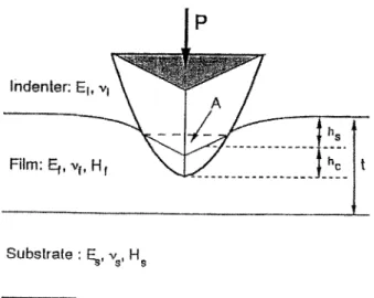
(iv)
Extraction of the hysteresis curve. (v) Correction for elastic recovery to determine the plastic depth, and then the hardness could be calculated. The physical processes involved are shown schematically in Fig. 1. ~ As the indenter is first driven into the film, both) unless CC License in place (see abstract). ecsdl.org/site/terms_use
address. Redistribution subject to ECS terms of use (see 140.113.38.11
3100
J. Electrochem. Soc.,
Vol. 142, No. 9, September 1995 9 The Electrochemical Society, Inc.elastic and plastic deformation occur. The plastic deforma- tion results in the formation of a permanent hardness im- pression t h a t conforms to the shape of the indenter to some contact depth, h~. The elastic processes result in an addi- tional component of displacement, one manifestation being that the surface displaces d o w n w a r d at the edge of the contact by an amount, h~. The key to the analysis procedure is that as the indenter is withdrawn, the elastic displace- ments are recovered, and an analysis of the elastic unload- ing data can then be used to relate experimentally m e a - sured quantities to the projected contact area and an effective elastic modulus. TM
Samples were mounted on a fixture which permits shift- ing them about the vertical axis to any desired position. All tests were carried out at ambient temperature (22.7~ and humidity with the instrument inside a thermally lagged enclosure in an air-conditioned room. The resultant ther- mal was better than 0.1~ over periods of several hours. All tests were performed at a nominal constant loading rate of 1.18 mN/s of the m a x i m u m set displacement. For each sam- ple, ten separated indents, spaced 15 i~m from each other, were made on the investigated surface.
The hardness, H, is given by
H = L~/A~ [1]
where Lm~ is the load corresponding to the total displace- ment, A~ is the projected contact area determinated by the geometry of the indenter. P h a r r and Oliver 8 proposed that the area function of a Berkovich indenter w i t h a perfect triangular p y r a m i d geometry is given by
Af = 24.5d 2 [2]
where d is the distance from the tip of the indenter, but for real indenters, Af must be corrected due to rounding at the tip. The projected contact area of a Berkovich indenter we used is proposed by the m a n u f a c t u r e ~9
A~ = 23.897d 2 [3]
Fourier transform infrared (FTIR) anaIysis.--Room tem- perature IR transmission measurements were performed in the wave number range from 4400 to 400 cm -1 using a Bio- rad QS300 FTIR spectrometer w i t h a CsI beam splitter. 256 scans were performed for every sample and the obtained spectra were averaged to increase the signal-to-noise ratio. Instrumental resolution was 4 cm -~. A prime, unprocessed substrate was used as the background to ensure that the spectra obtained was solely due to S i Q films.
Results
Nanoindentation measurement of undoped dielectric films.-- The nanoindentation technique is a powerful tool for examining both the deformation response and deforma-
I n d e n t e r : El, vt
Film: El, ~,~, Hf
I
tSubstra~e : Es, ~, H s
Fig. 1. The physical processes involved in the indentation of a thin film on a substrate. 8
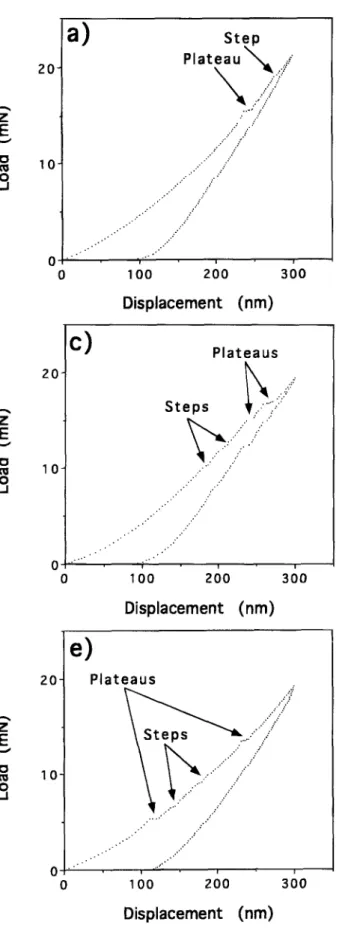
tion mechanism transition exhibited by ceramic materials in response to fine-scale surface contacts.13 The remarkable change of mechanical properties due to different film depo- sition processes is best illustrated by examples like Fig. 2. The same m a x i m a l displacement (300 nm) was applied in all cases, but the final loads for harder coatings were larger than those for softer coatings.
Crack resistance estimation from the loading curve.--For
the brittle coatings on silicon, the deformation of the coat- ing often has a large elastic component. Indeed, for inden- t e r displacements up to about 50 nm the deformation can be purely elastic and therefore totally reversible. 16 In Fig. 2 t h e loading curve exhibits small steps and plateaus. These are not thought to be related to difference in elastic rood- ulus between the coating and the substrate as they are too sudden. T h e m o s t likely interpretation of these events is that they represent the propagation of various types of cracks, either t h r o u g h the coating ("through-thickness cracks," caused b y flexure of the coating) or along the coat- ing-substrate interface (caused b y shear stresses across the interface), a w a y f r o m the i m m e d i a t e contact zone w h e r e the coating is flexed into conformity with the surface of the indenter.16
T h e precursor cracks for S i H 4 - A P C V D films, as c o m - p a r e d with other dielectric films, a p p e a r e d at an earlier stage of indentation, a n d this event d e m o n s t r a t e d that a discontinuous increase in penetration depth clearly oc- curred as the plastic flow w a s initiated. In order to inter- pret observations in crack initiation of studied dielectric films, a crack resistance ( C R ) p r o p o s e d b y A. K. S i n h a et
al. 19 w a s used as a criteria. A dielectric film with a lower C R value tends to crack at lower applied stress. T h e C R is defined as 19
CR = ~p ~u - ~ [4]
Po
where p and po are structurely "imperfect" and "perfect" dielectric film density, respectively, au is the ultimate ten- sile stress of a structurely "perfect" dielectric film, and ~m is the measured residual stress of the studied film.
Calculation of relative CR of various dielectric films could be made for S i Q . Since the density of various SiO2 films are all around 2.2 g/cm ~ which is assumed as a refer- ence density value for amorphous SiO2, the CR of SiO2 films is determined solely by the residual stress term. The resid- ual compression stress suppresses cracks initiating during the loading cycle ~1 and vice versa. Therefore the occurrence of cracks was seen during low-load indentation as Sill4- APCVD film (Fig. 2e) had a residual tensile stress. As shown in Fig. 2a-d, the SiO2 films w i t h compressive resid- ual stress do have a higher load at the initiation of cracks than a film w i t h tensile stress.
Hardness calculation from the unloading curve.--The
hardness values were determined from the slopes of the first 20 % of the unloading sections. It was clearly observed from Table I that the hardness of thermal oxide film was higher than that of the CVD films. This demonstrates t h a t the hardness of dielectric films is closely related to the film's preparation m e t h o d s . A l t h o u g h SiO~ films, whether grown by the oxidation of silicon or deposited by CVD pro- cesses, have an amorphous structure with a random net- w o r k of polyhedral, 17 CVD silicon dioxide, depending on the deposition conditions, may have a lower density and slightly different stoichiometry from thermal oxide, caus- ing changes in mechanical and electrical films properties (such as hardness, stress index of refraction, etch rate, dielectric constant, and high electric-field breakdown strength).17 The direct p a r a m e t e r affecting those properties to be considered is then the Si-O bond density (Ns~_o), as discussed in the following section.
Relationship between hardness and Si-O bond density of undoped oxide films.--In order to correlate the studied un- doped SiO2 films' mechanical properties to their micro- structures, FTIR was used to analyze oxide films prepared by different methods, including t h e r m a l oxidation, SiH~-
) unless CC License in place (see abstract). ecsdl.org/site/terms_use
address. Redistribution subject to ECS terms of use (see 140.113.38.11
J. Electrochem. Soc.,
Vol. 142, No. 9, September 1995 9 The Electrochemical Society, Inc.
3101
z
E
"O O ..J20"
1 0
0
0
!a)
Step
P l a t e a u ~
. c\ /
J"i/
/ Y .,:" / ./" /" ., .."" / : it.."100
200
z
E
Displacement (nm)
"Oo
J2 0
1 0
0
i300
0
b)
P l a t e a u
~
yl;S/?~
.-"" ..:"S t e p
. . ' , - ,' ," .' .'" .'" ," "" ,- . . / f " : .,.: F : .... ." . . .,'" ,.. ... . , . ' " i" i i100
200
300
Displacement (nm)
z
E
V " 0 O ..Jc)
20-
10-
0 "" ""0
100
P l a t e a u s
S t e p s~."~:,,?:/
,.,' ..." . ' .: i i200
300
Displacement (rim)
Z
E
V "O 0= O . d20
d)
10
. . . ' .,.."0
S t e p s
P l a t e a U ( / f
./,'" i i100
200
300
Displacement (nm)
z
E
"O (I= O ..J20
10
e)
P l a t e a u s
.." .Y . , .. i I0
100
200
300
Fig. 2. Load-displacement curve for dielectric films on silicon sub-
strate (a) thermal oxide; (b) SRO-PECVD film; (c} TEOS-PECVD film; (d)
SiH4-PECVD film; (e) SiH4-APCVD film.
Displacement (nm)
P E C V D , T E O S - P E C V D , a n d S i H 4 - A P C V D . Figure 3 is a stacked plot of the transmission spectra obtained for the various u n d o p e d S i Q films. T h e b a n d s d u e to the a s y m - metric St-O-St a n d S t - O H stretching vibration are nor- m a l l y in the r a n g e ii00 to i000 c m i a n d 3200 to 3700 c m -I, respectively. 2~ T h e p e a k position of these t w o b a n d s w e r e influenced b y b o n d i n g environment, stoichiometry, density a n d porosity of the SiOx films. T h e O - H b o n d stretching in S t - O H structures giving rise to absorption b a n d s at a b o u t 3600 c m -I is observed for C V D fihns, but it is absent in t h e r m a l oxide films. O n the other hand, the S i - O absorp- tion p e a k of the t h e r m a l oxide film is located at
1091.9 c m -I, w h i l e the S i - O a b s o r p t i o n p e a k for T E O S - P E C V D a n d S i H 4 - A P C V D films a p p e a r at l o w e r w a v e n u m b e r s , 1076.6 a n d 1078.4 c m -i, respectively, a n d that of S ~ H 4 - P E C V D films a p p e a r s in a n e v e n l o w e r w a v e n u m b e r , 1059.5 c m i. E s t i m a t e s of the density of o x y g e n b o n d e d to silicon h a v e b e e n o b t a i n e d f r o m the integrated a b s o r b e n - cies of the S i - O stretching m o d e s 9 A c c o r d i n g to Ref. 22 a n d 23, the concentration values w e r e e s t i m a t e d as follows
2.303Bs
Nsi_o - $ A ( v ) d v
<v>t J [5"
) unless CC License in place (see abstract). ecsdl.org/site/terms_use
address. Redistribution subject to ECS terms of use (see 140.113.38.11
3102
J. Electrochem. Soc., Vol. t42, No. 9, September 1995 9
The ElectrochemicalSociety, Inc.
200 u e-. .i.JE lOO
r- Si-OH ' ' Si O"
.cvo
_TEOS-PECVD~
Thermal Oxide ~ 4000 3000 2000 1000Wavenumber (cm-1)
Fig. 3. Stacked plot of the transmission spectra for thermal oxide, SiH4-PECVD, TEOS-PECVD, and SiH4-APCVD films.
where Ns~-o is the n u m b e r of Si-O bonds per cubic centime- ter, B s (the inverse cross section) used for Si-O(s) mode is 1.5 • 10 ~9 cm -2, v is the wave n u m b e r of the incident radia- tion, <v> is the wave n u m b e r at which the Si-O stretch is at a maximum, A (v) is the absorbance, a n d t is the thickness of the films. The Ns~_o of PECVD films made from silane is about 2.92 • 102~ bonds/cm 3, a n d PECVD films obtained from TEOS is about 4.42 • 1022 bonds/cm 3. For thermal oxide and SiH%APCVD films, the Nsi_ o is 8.82 • 1022 a n d 4.38 • 1022 bonds/cm 3, respectively.
The higher Ns~-o value of thermal oxide films compared to CVD films can be explained by the hydrogen incorporation in the CVD films. Indeed, hydrogen atom impurities incor- porated into CVD films form Si-OH hydrogenated bonds, as evidenced by FTIR analysis, and consequently reduce the total Si-O bond density. In addition to the hydrogen incorporation, the presence of defects, microvoids, cluster- ing, a n d d a n g l i n g b o n d s could affect the Si-O b o n d density. Furthermore, Fig. 3 shows changes of the m a x i m u m Si-O absorption peak for CVD films. The possible contributor to the shift in the Si-O asymmetric stretching frequency is related to a continuous shift in the Si-O-Si b o n d angle. 24 The Si-O-Si b o n d angle is influenced by ~ b o n d i n g interac- tions between n o n b o n d i n g oxygen p states a n d empty Si d states. The Si-O-Si b o n d angle increases as the average n u m b e r of oxygen atoms bonded to a given silicon atom is increased, a n d this contributes to the observed shifts in the frequency of the asymmetry stretching vibration for the CVD S i Q films. 40 A 3 6 a.
O
32r
e- "O 28 "1" 24 209
Thermal Oxide
_ . ~
9
TEOS-PECVD
~ / / / I
o S ! H , - A P C V D / ~ I I v , 2 4 6 8 1 0B o n d i n g d e n s i t y (10 zz bonds/cm 3)
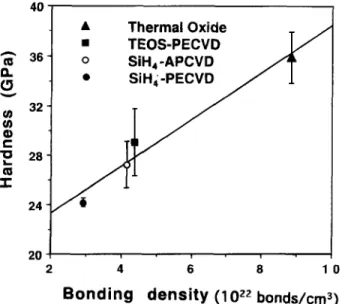
Fig. 4. Linear relationship of the hardness on the Si-O bond density for oxide films.
Figure 4 indicates that the hardness scale up with the Si-O bond density of the various undoped SiO2 films. By fitting the various undoped SiO2 film data, the hardness, H, could be expressed as a linear function of the Si-O b o n d density in the studied range, as follows
H = 19.518 + 1.8886 X Nsi_ o [6] where H a n d Nsi-o are with units in GPa a n d 1022 bonds/cm 3, respectively. This linear dependence of hardness on b o n d - ing density correlates well with the results of the study by E1 K h a k a n i e t al. 24 who found the same trend for a-SiC thin films. An increase of the Si-O bond density will lead to an enhancement of the cross-linkage of Si a n d O atoms, result- ing in a strengthened amorphous SiO2 material frame a n d ultimately a n improved hardness. It is worth noting that the upper limit of the Si-O b o n d density is reached in crys- talline (ordered form) S i Q films, which consequently pre- sent the highest hardness. I n amorphous SiO2 films that are structurally disordered, the f u n d a m e n t a l cell ("elemen- tal spring") in the amorphous network, from a mechanical viewpoint, is the Si-O bonds. Thus, the hardness of the amorphous network is directly related to the density of the Si-O bonds.
T h e r e l a t i o n b e t w e e n h a r d n e s s a n d r e m o v a l r a t e o f v a r i - o u s d i e l e c t r i c f i I m s . - - A more complete removal model, proposed by Runnels and Eyman, ~ would be of the form removal rate ( R . R . ) R . R . = f(~, ~), where a a n d 9 are the magnitudes of the normal and shear stresses, respectively, on the wafer surface. They considered this model be an analogy to Preston's equation 25
R . R . = tc X (r X ~ [7] The development a n d use of such models requires the determination of stress distributions. Although the com- plex change in stress distribution is not realized, it can be inferred that both normal and shear stress dominate abra- sion of the wafer surface. Because the variation in pad wear conditions a n d slurry distribution during polishing at dif- ferent runs causes the abrasive contact change, the removal rate of the dielectric material therefore fluctuates during different runs regardless of whether the same polishing conditions are present. Consequently, i n order to eliminate removal rate variation from r u n to run, the removal rate ratio ( R . R . ratio) is defined as
Removal rate of dielectric film
R . R . ratio =
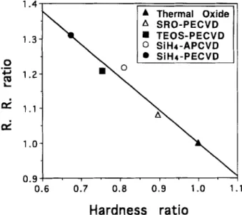
Removal rate of thermal oxide The role of the slurry particles is to add a chemical "tooth" to the polishing process, 2 a n d the bond strength between the slurry particle a n d wafer surface will deter- mine the mechanical cutting efficiency of the dielectric film surface. Thus, the strength a n d hardness of the polished films have a great influence on the wear mechanism in the CMP process. Since the surface mechanical properties of the various dielectric films are different, it is obvious that different dielectric films will exhibit different material re- moval behavior at the same run. This suggests a potentially important relationship between the removal rate a n d the surface mechanical properties of the wafer. Figure 5 clearly shows that the polishing rate of the various dielectric films is inversely proportional to its hardness
R . R . ratio = 1.94 - 0.94 • hardness ratio [8] where
hardness of dielectric film Hardness ratio =
hardness of thermal oxide The above relation indicates that high hardness results in a low removal rate for the undoped oxide film. Similar relationships were observed for removal rates vs. the mi- crohardness of the leached surface in Izumitani's study. ~7 Furthermore, Cook 26 has reviewed the mechanics and chemical process of glass polishing. He proposed that re- moval rate is inversely proportional to the modulus, E, of
) unless CC License in place (see abstract). ecsdl.org/site/terms_use
address. Redistribution subject to ECS terms of use (see 140.113.38.11
J. Electrochem. Soc.,
Vol. 142, No. 9, September 1995 9 The Electrochemical Society, Inc. 3103 O . m I = - -,4
,4
1:]
1. 1.2 1.1 1.0 0.9 0.6 \ 9 Thermal Oxide A S R O - P E C V D " ( K 9 T E O S - P E C V D O S i H 4 - A P C V D @ S i H 4 - P E C V D 0.7 0,8 0.9 1.0 .1Hardness ratio
Fig. 5. Linear relationship of the normalized removal rate (R.R.) on the normalized hardness for various dielectric films.
glass a n d the w a t e r in the slurry chemically reacts with silicon dioxide. T h e reaction proceeds as follows
-= St-O-St -= + H20 ~ 2 -= St-OH
However, the diffusion coefficient of water in silica, which is believed to be the rate-controlling factor of this reaction, is quite low. Hence, the chemical process may not play as much of a role as the surface mechanical factors in deter- m i n i n g CMP polish rate for undoped oxide films. Modulus as well as hardness could be the determining factor of re- moval rate i n this case. G i l m a n 27 has shown that the micro- hardness of structural materials usually increases linearly with an increase in modulus, a n d the H/E ratio is about 1/10 for most covalently bonded materials. These two sce- narios together with our experimental findings seem to suggest that the hardness d e p e n d e n c e of r e m o v a l rate is actually justified through the h a r d n e s s - t o - m o d u l u s ratio
H / E . D e v e l o p m e n t of a n e w m o d e l that provides linkage
b e t w e e n C M P r e m o v a l rate a n d m e c h a n i c a l factor (e.g.,
H / E ratio) is currently underway. ~8
It m u s t be e m p h a s i z e d that this linear relationship is ef- fective only in the well-controlled polishing region. T h e linear relationship w o u l d disappear because glazing of p a d surface a n d inadequate p a d conditioning lead to a different degree of decrease in r e m o v a l rate.
A s Eq. 6 a n d 8 predict, an increase in the n u m b e r of Si-O b o n d s (and b o n d density a s s u m i n g constant volume) strengthens the oxide film, leading to higher hardness value a n d hence lower r e m o v a l rate. Desai et al. 89 reported that increasing the 02 content in the reaction gas mixture led to a significant increase in the r e m o v a l rate of their SiO= films deposited b y the E C R p l a s m a C V D m e t h o d . It w a s a s s u m e d that as the O2 partial pressure in the c h a m b e r w a s increased, the reaction, 2 O2 + Sill4 --> SiO~ + 2 H 2 0 , w a s favored. T h e presence of excess O8 w o u l d result in the for- m a t i o n of H20. Consequently, it w a s possible that the H 2 0 f o r m e d during the deposition process tended to be incorpo- rated in the film as H20, S t - O H , or S i - H resulting in the decrease of the Si-O b o n d i n g density a n d the increase in the r e m o v a l rate of their SiOx films.
Conclusions
The n a n o i n d e n t a t i o n technique is a powerful tool for ex- a m i n i n g the deformation exhibited by various t h i n - f i l m materials in response to fine-scale surface contacts. The surface mechanical properties of the undoped dielectric films presented here were determined by n a n o i n d e n t a t i o n . Crack resistance of the various dielectric films were exam- ined from the loading curve. E x p e r i m e n t a l results show that crack initiation for SiH4-APCVD films with a tensile stress, as compared with other dielectric films with c o r n -
pressive stresses, occurs during the l o w - l o a d indentation. T h e hardness of dielectric films w a s d e t e r m i n e d f r o m the unloading section. It is p r o p o s e d that the C V D oxide films with a m o r e o p e n structure w o u l d h a v e lower hardness. Moreover, F T I R mierostructure analysis s h o w e d that the estimated Si-O b o n d densities of the u n d o p e d oxide films prepared b y different m e t h o d s exhibited a linear variation with the film hardness. T h e different material r e m o v a l be- havior could be attributed to the varied surface m e c h a n i c a l properties of the u n d o p e d films. T h e C M P r e m o v a l rate for the various S i Q films w a s f o u n d to exhibit a linear depen- dence on their hardness. A simple perspective whichrelates r e m o v a l rate to the m e c h a n i c a l factor H I E is p r o p o s e d to account for this observation. B a s e d on this perspective, it is suggested that a linear relationship is reasonable b e t w e e n the surface hardness a n d the r e m o v a l rate of the u n d o p e d dielectric films in the well-controlled C M P process. This linear relationship m a y disappear d u e to p a d glazing a n d inadequate p a d conditioning w h i c h lead to a different de- gree of decrease in r e m o v a l rate.
Acknowledgment
T h e authors express appreciation for helpful discussions with Dr. T. Y. Y e n in the Institute of M e c h a n i c a l Engineer- ing, National Chiao T u n g University. This w o r k is sup- ported b y U M C , T S M C , a n d National Science Council ( N S C 8 3 - 0 4 2 5 - E 0 0 9 - 0 0 1 - 3 ) , R.O.C. W e t h a n k the Precision Instrument D e v e l o p m e n t Center for providing the N A N - O T E S T 500 used for these experiments.
M a n u s c r i p t submitted Oct. 6, 1994; revised m a n u s c r i p t M a y i0, 1995.
The National Nano Device Laboratory assisted in meet- ing the publication costs of this article.
REFERENCES 1. P. Singer, Semicond. Int., 17, 48 (1994).
2. S. Sivaram, H. Bath, R. Leggett, A. Maury, K. Monnig, a n d R. Tol]es, Solid State TechnoI., 35, 87 (1992). 3. P. H. Singer, Semicond. Int., 15, 44 (1992).
4. J. Warnock, This Journal, 138, 2398 (1991).
5. R. Kolenkow and R. Nagahara, Solid State Technol.,
35, 112 (1992).
6. S.R. Runnels and L. M. Eyman, This Journal, 141, 1698 (1994).
7. C. W. Pearce, i n VLS[ Technology, S. M. Sze, Editol, Chap. 1, pp. 9-54, McGraw Hill Book Co., New York (1988).
8. G. M. Pharr a n d W. C. Oliver, M R S Bull., 8, 28 (1992). 9. R. Nowak a n d M. Sakai, J. Mater. Res., 8, 1068 (1993). 10. J. B. Pethica, R. Hutchings, a n d W. C. Oliver, Philos.
Mag., 48, 593 (1983).
11. R. Tandon, D. J. Green, a n d R. E Cook, J. Am. Ceram. Soc., 73, 2619 (1990).
12. G.M. Pharr, W. C. Oliver, R. F. Cook, P. D. Kirchnel, M. C. Kroll, T. R. Dinger, a n d D. R. Clarke, J. Mater. Res.,
7, 961 (1992).
13. T. E Page, W. C. Oliver, a n d C. J. McHargue, ibid., 7,450 (1992).
14. X. Jiang, M. Wang, K. Schmidt, E. Dunlop, J. Haupt, a n d W. Gissler, J. Appl. Phys., 69, 3053 (1991). 15. D. Li, Y. W. Chung, M. S. Wong, a n d W. D. Sproul, ibid.,
74, 219 (1993).
16. A. J. Whitehead a n d T. E Page, Thin Solid Film, 220, 277 (1992).
17. S. Wolf a n d R. N. Tauber, Silicon Processing for the VLSI Era, Lattice Press, Sunset Beach, CA (1986). 18. M. F. Doerner a n d W. D. Nix, J. Mater. Res., 1, 601
(1986).
19. A. K. Sinha, H. J. Levinstein, a n d T. E. Smith, J. Appl. Phys., 49, 2423 (1978).
20. G. Socrates, Infrared Characteristic Group Frequen- cies, John Wiley & Sons, Inc., New York (1980). 21. D. K. Basa a n d E W. Smith, Thin Solid Films, 192, 121
(1990).
22. S. Rojas, L. Zanotti, A. Borghesi, A. Sassella, a n d G. U. Pignatel, J. Vac. Sci. Technol., Bll, 2081 (1993). 23. G. Lucovsky, S. Y. Lin, P. D. Richard, S. S. Chao, Y.
Takagi, P. Pat, J. E. Keen, a n d J. E. Tyler, J. N o n -
Cryst. Solids, 75, 429 (1985).
24. M. A. E1 Khakani, M. Chaker, A. Jean, S. Boily, J. C. ) unless CC License in place (see abstract). ecsdl.org/site/terms_use
address. Redistribution subject to ECS terms of use (see 140.113.38.11
3104
J. Electrochem. Soc.,
Vol. 142, No. 9, September 1995 9 The Electrochemical Society, Inc.Kieffer, M. E. O'Hern, M. F. Ravet, and F. Rousseaux,
J. Mater. Res.,
9, 96 (1994).25. F. Preston,
J. Soc. Glass Technol.,
11 (1927). 26. L. M. Cook,J. Non-Cryst. Solids,
120, 152 (1990). 27. J. J. Gilman,Mechanical Behavior of Crystalline
Solids,
National Bureau of Standards Monograph,59, 79, Washington, DC (1963).
28. C.W. Liu, W. T. Tseng, B. T. Dai, and C. F. Yeh, In prepa- ration.
29. M. Desai, R. Carpio, R. Jairath, M. Stell, and R. Tolles, Paper presented at Materials Research Society Sym- posium, Boston, MA, Nov. 29-Dec. 2, 1993.
Adsorption Species of Transition Metal Ions on
Silicon Wafer in SC-1 Solution
Yoshihiro Mort, Kenichi Uemura, and Kengo Shimanoe
Nippon Steel Corporation, Electronics Research Laboratories, 3434 Shimata, Hikari, Yamaguchi 743, Japan
ladashi Sakon
Nippon Steel Corporation, Advanced Materials and Technology Research Laboratories,
1618 Ida, Nakahara-ku, Kawasaki, Kanagawa 211, Japan
ABSTRACT
Adsorption of t r a n s i t i o n metal ions such as Fe(III), Ni(II), a n d Zn(II) on silicon wafers in ammoniac hydrogen peroxide solution (SC-1 solution) has been studied. It was found by comparing the experimental results with the equilibrium calculations that the m a i n adsorption species is the dissolved n e u t r a l hydroxide complex. This was supported by t h e calculated free energy change of adsorption of hydroxide complexes.
Introduction
It is well k n o w n that surface c o n t a m i n a t i o n of silicon wafers, from metal ions and particles, deteriorates electri- cal properties of large scale integrated circuit (LSI) prod- ucts. In order to reduce such c o n t a m i n a t i o n introduced from the environment a n d equipment, m a n y kinds of clean- ing solutions have been developed a n d used. SC-1 solution (29% NH4OH:31% It202:H20 = 1:1:5 volume ratio) 1 is one of the widely used cleaning solutions i n semiconductor m a n u - facturing. It offers very high particle removability relative to other cleaning solutions like SC-2 (35% HCl:31% H202:H20 = 1:1:5 volume ratio) a n d DHF (50% HF:H20 = 1:99 volume ratio). 1 At the same time, however, surface metal c o n t a m i n a t i o n is caused by some metal impurities in the solution. 2 Metal impurities, especially transition metals, cause electrical deterioration such as gate oxide b r e a k d o w n ? Some improvements such as the addition of chelating agents 4 have been made to reduce the metal ion adsorption on a silicon wafer surface. There have also been several efforts to explain the metal adsorption mecha- nisms. Ryuta
et al.
investigated the kinetics of metal ion adsorption a n d estimated adsorption a n d desorption coef- ficients for some transition metals. 5 But they did not m e n - tion the adsorption species. Hiratsukaet al.
investigated metal ion adsorption as a function of pH and proposed that the adsorption species of A1 is the hydroxide complexes. 6 But they did not discuss the adsorption species of t r a n s i - tion metals. To clarify the adsorption species of transition metal ions in SC-1 solution is of importance for the under- standing of the cleaning mechanism a n d the development of new cleaning solutions.When a silicon wafer is immersed in an SC-1 solution, the wafer is etched continuously. Though the etching seems to affect the adsorption behavior of metal ions as well as ad- sorption equilibria, we do not take it into account in this study. The reason is as follows: although the etching rates of bare a n d thermally oxidized silicon wafers are quite dif- ferent, the adsorption behavior of transition metal ions onto the wafers is almost the same. 7 In the present study, we have investigated the adsorption behavior by means of e q u i l i b r i u m analyses. The analyses have been used to assign the adsorption species. Free energy calculation of
adsorption has also been performed to know the adsorp- tion species a n d to support the results of equilibrium a n - alysis. The metal ions examined in this work are Fe(III), Ni(II), a n d Zn(II) as typical c o n t a m i n a n t s in semiconductor manufacturing.
Experimental
Sample preparation.--The
wafers used in the present work were polished silicon single crystals with a (100) face. Both p- a n d n-type wafers with a conductivity range of 8 to 12 Ft cm were used. The wafer diameter was 125 mm a n d the thickness was 500 to 600 ~m.The schematic of the sample preparation process is shown in Fig. 1. The wafers were dipped in an HF-H202- H20 cleaning solution 8 for i0 m i n to remove initial metal contamination. Then they were rinsed in deionized water a n d dried with a spindrier. They were subsequently im- mersed in the testing SC-1 solution (29% NH4OH:31% H~O2:H20 = 1:1:5 volume ratio) for 10 m i n at 80~ rinsed in deionized water, a n d dried with a spindrier. A certain a m o u n t of standard solution which contains t r a n s i t i o n metal ions of Fe(III), Ni (II), or Zn(II) was added to make the c o n t a m i n a n t level of the SC-1 solution 10-9-10 -4 mol 1-1. Tetramethylammonium hydroxide was used to raise the pH of the SC-1 solution if necessary.
The following chemicals used in this work were EL grade which contain t r a n s i t i o n metal impurities below 0.5 ppb: 50% HF, 29% NH4OH, 31% H202, 20% tetramethylammo- n i u m hydroxide. Metal standard solutions (1000 ppm) for atomic absorption spectrophotometry (AAS) were used for the i n t e n t i o n a l contamination. The deionized water used in this work contains t r a n s i t i o n metal impurities below 10 ppt.
All the processes were carried out in a class 100 clean room, a n d wet chemicals were treated inside a clean draft in the room.
A A S and TXRF measurements.--Surface
metal concen- tration on a standard sample for total reflection x-ray fluo- rescence spectrometry (TXRF) was assigned b y determin- ing the a m o u n t of metals on another wafer treated in the same batch, using a graphite furnace (GF) AAS (Perkin- Elmer Z-5100). In the GF-AAS measurement, surface) unless CC License in place (see abstract). ecsdl.org/site/terms_use
address. Redistribution subject to ECS terms of use (see 140.113.38.11