國
立
交
通
大
學
電機學院 電機與控制學程
碩
士
論
文
0.5 微米 500 伏特 99.65% 高感應精準度傳感預測器
之電氣隔離充電器應用
Open-Loop Trans-Predictor with 99.65% Battery Voltage Accuracy
for Electrical Isolation AC Charger System in 0.5µm 500V BCD
Process
研 究 生:林浩元
指導教授:陳科宏 博士
0.5 微米 500 伏特 99.65% 高感應精準度傳感預測器之電氣隔離充電器應用
Open-Loop Trans-Predictor with 99.65% Battery Voltage Accuracy for Electrical Isolation AC Charger
System in 0.5µm 500V BCD Process
研 究 生:林浩元 Student:Hao-Yuan Lin
指導教授:陳科宏 Advisor:Ke-Horng Chen
國 立 交 通 大 學
電機學院 電機與控制學程
碩 士 論 文
A ThesisSubmitted to College of Electrical and Computer Engineering National Chiao Tung University
in partial Fulfillment of the Requirements for the Degree of
in
Electrical and Control Engineering November 2013
Hsinchu, Taiwan, Republic of China
中 華 民 國 一零二 年 十一 月 十一 日
0.5 微米 500 伏特 99.65% 高感應精準度傳感預測器之電氣隔離充
電器應用
學生: 林浩元 指導教授: 陳科宏 博士
國 立 交 通 大 學 電 機 學 院 電 機 與 控 制 學 程 碩 士 班
摘要,
在現今社會,可攜式產品已經成為人人不可或缺的必備工具。隨著電子產品的蓬勃發 展,可充電電池也成為目前最適合可攜式產品使用的行動電源。因此,如何以最理想且 安全的方式將能量傳遞到電池,對電池進行最快速也最有效率的充電是一個重要的課 題。在電池到充電器之間所產生寄生電阻等非理想效應會對充電器判斷輸出電壓大小造 成不小的影響,進而影響充電器的效能。本文所提出之開迴路控制器是一種高效率而且 低成本的充電器,同時也是一種能容忍市電的高輸入電壓隔離式充電器。但是此控制器 與一般控制器最大的分別就是它並沒有直接的迴授路徑來獲取輸出電壓資訊,因此如何 準確從輔助繞組中去取得輸出電壓資訊同時排除上述非理想效應所造成的影響,進而準 確控制整個系統變成一個重要問題。此外,為了確保充電器在定電流充電模式與定電壓 充電模式皆能保持穩定且平穩切換,本切換式充電器將定電流充電迴路與定電壓充電迴 路並聯,且同時達到兩者的穩定性。 本篇論文完成一具有排除非理想效應的電池電壓精準偵測電路。不同於以往的方 式,這次提出的偵測電路不僅能準確的偵測電池電壓,並不需要外部原件來做修正,同 時也使所有的控制路徑在定電流充電模式與定電壓充電模式皆能保持穩定且平穩切 換。為了使效率更進一步提升,波谷切換以及動態頻率切換被應用在定電壓充電模式。Open-Loop Trans-Predictor with 99.65% Battery Voltage Accuracy for
Electrical Isolation AC Charger System in 0.5µm 500V BCD Process
Student: Hao-Yuan Lin Advisor: Dr. Ke-Horng Chen
Degree Program of Electrical and Computer Engineering
National Chiao Tung University
ABSTRACT
Electronic devices in all kinds of fields have been requested to run after perfection in terms of every aspect in recently. Nowadays, most of household appliances and portable devices in use are directly connected to the supply via plugs and sockets to get activated or to charge its built-in battery. With the rapid growth in the consumer electronics, rechargeable mobile battery bank has proved to be the most compatible for portable devices. The proposed open-loop regulator is a high efficiency and low cost solution for power applications, and it is also a high input voltage isolated charger compatible with AC supply. However, the biggest difference between the proposed and general regulators is that the proposed has no direct feedback loop to obtain output information. Hence, it’s a major challenge to precisely detect the battery voltage from auxiliary winding, and thus to accurately control the entire system.
This proposed open-loop regulator charger excludes non-ideal effects from the practical battery. Besides, the proposed technique detects battery voltage precisely without any feedback network and has all control paths stabilized and switched smoothly under constant voltage and constant current modes. Valley switching and dynamic frequency switching are both set and applied in the constant voltage mode in order to pursue high efficiency and performance.
誌謝
誌謝
誌謝
誌謝
時間過得好快,兩年的碩士班生涯,轉眼間就要告一段落了,衷心感謝在碩士班期 間曾經幫助過我的大家,在此,要一一表達我對您們的感謝。首先要感謝我的指導教授 陳科宏博士,我一直都覺得能當老師的指導學生,真的是一件很幸運也很榮幸的事,謝 謝老師在研究上對我的指導,您開明的指導方式,讓我能盡情發揮我的想法,謝謝您總 是會抽出時間與我討論研究上的問題,即使是很初淺的問題,您也會很仔細的回答,讓 我能夠很紮實的奠定基礎,謝謝您日常生活上的照顧,老師的關心雖然有時並不直接, 但我總能感受到,並且都會使我的心都會暖暖的,真的真的非常謝謝老師。 感謝912 實驗室的全體夥伴們在研究生活中的互相扶持。感謝學長姐輝哥、斤哥、 期哥、中中、契哥、昭彰、蘇蘇、雅萍、夸克、GM、大龍、之璞、。感謝有你們在學業 上與生活上的照顧與指導。 感謝同儕下巴消失的 PONY、BONBON、祖為、亞當、紹祥,與你們一起 meeting、畫 layout、一起討論問題、一起瘋狂,一起唱歌、一起運動,這些都是我的碩士班期間的 珍貴回憶。感謝學弟們孟狗、D 狗、狗杰、多狗、狗屁、油狗、宅男柚弛,你們的垃圾 嘴是最棒的,實驗室有了你們的加入後,也創造了實驗室有史以來最大經濟成長! 在此,特別要感謝昭彰與中中兩位博班學長,點點滴滴難以逐字勾勒出你們對我的 照顧,不僅在課業上,在日常生活上,也能感受到對我的照顧。在碩士班能遇到像你這 樣的學長們,真的是我的福氣。 最後感謝我的父母與家人,有你們的鼓勵與幫助,才能讓我能無憂無慮順利的完成 碩士學業。雖然我不擅表達,但我真的感謝你們。 僅以此論文獻給我愛的人及愛我的人,家人們、同學們、朋友們和所有關心我的人。 因為有你們,使本論文豐富不少,謝謝你們。Contents
CHAPTER 1 ... 1
INTRODUCTION ... 1
1.1 THE BASIC CONCEPT OF THE ISOLATED CONVERTER ... 2
1.1.1 Architecture of Asymmetrical Isolated Converters ... 4
1.1.2 Architecture of Symmetrical Isolated Converters... 7
1.2MOTIVATION ... 11
1.3THESIS ORGANIZATION ... 13
CHAPTER 2 ... 14
THE CHARGER SYSTEM WITH THE PROPOSED TRANS-PREDICTOR ... 14
2.1THE NON-IDEAL EFFECT OF PRACTICAL BATTERY ... 15
2.2THE PRINCIPLES OF THE PROPOSED CHARGER SYSTEM WITH TRAN-PRECDICTOR ... 18
2.3THE BASIC OPERATION OF FLY-BACK BASED CONTROLLER IN CHARGER SYSTEM ... 19
2.3.1 The Operation of the Flyback System ... 21
2.3.2 The Output Current Calculation ... 24
2.3.3The Constant Current Loop, Constant Voltage Loop and Siwtching Frequency ... 25
CHAPTER 3 ... 27
THE CIRCUIT IMPLEMENTATIONS ... 27
3.1THE TRANS-PREDICTOR ... 27
3.2THE CURRENT TRANS-RUNNER ... 30
3.2THE LOOP SELECTOR ... 32
3.3PROTECTION MECHANISMS ... 33
3.4THE POWER COMPENSATINO ... 34
CHAPTER 4 ... 36
SYSTEM STABILITY ANALYSIS ... 36
CHAPTER 5 ... 43
EXPERIMENTAL RESULTS ... 43
5.2EXPERIMENTAL RESULTS ... 46
CHAPTER 6 ... 52
CONCLUSIONS AND FUTURE WORK ... 52
6.1CONCLUSIONS ... 52
6.2FUTURE WORKS... 52
FIGURE CAPTIONS
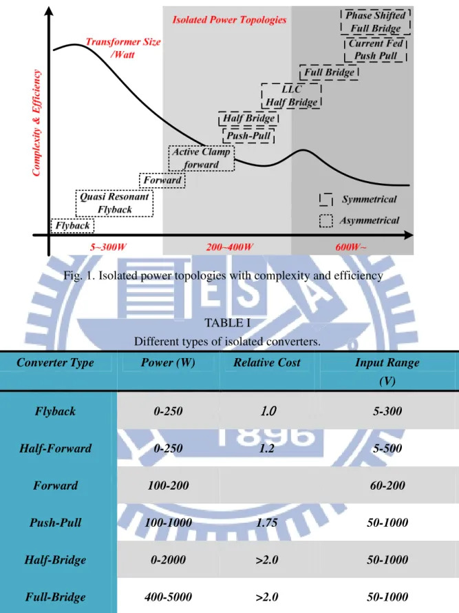
Fig. 1. Isolated power topologies with complexity and efficiency ... 3
Fig. 2. Flyback converter. ... 5
Fig. 3. Forward converter. ... 6
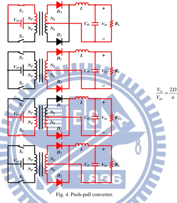
Fig. 4. Push-pull converter. ... 8
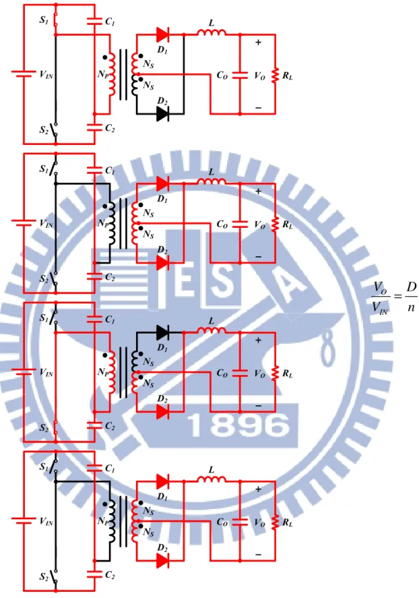
Fig. 5. Half-bridge converter. ... 9
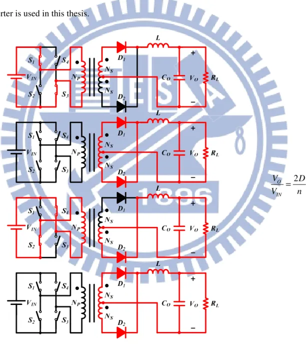
Fig. 6. Full-bridge converter. ... 10
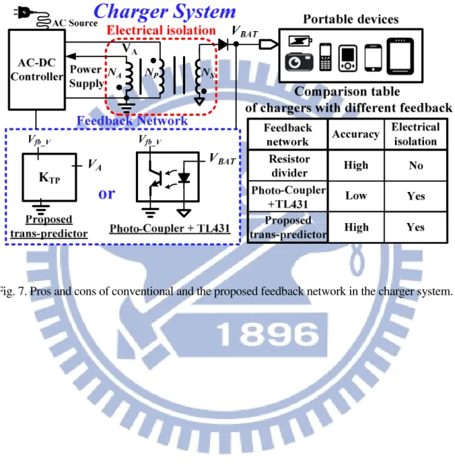
Fig. 7. Pros and cons of conventional and the proposed feedback network in charger system. .... 12
Fig. 8. (a) The real battery compositions and the BIR effect along with the charging path. (b) The causal relationship between drop effect and state of charge (SOC)... 17
Fig. 9. The architecture of flyback-based electrical isolation charger system with ... 19
Fig. 10. (a) Charging period. (b) Discharging period. (c) Resonant period. (d) The drop effect and the resonant effect.. ... 23
Fig. 11. An overview of the charger system in terms of operating mode and switching frequency from battery low to battery high. ... 26
Fig. 12. (a) the proposed trans-predictor technique and (b) the timing diagram of its operation.. 29
Fig. 13. (a) the circuit implementation of current trans-runner and (b) the timing diagram of its operation.. ... 31
Fig. 14. Loop selector for transitions between CC mode and CV mode………...32
Fig. 15. The protection mechanisms ... 33
Fig. 16. The adaptive input power limit protection for universal input range. (a) the adaptive input power limit selection and (b) the circuit implementation of power compensation... ... 35
Fig. 17. Small signal model with (a) the block diagram and (b) the compensation network.. . 37
Fig. 18. (a) Chip micrograph. (b) Prototype.. ... 39
Fig. 20. (a) Chip micrograph. (b) Prototype.. ... 44 Fig. 21. The efficiency of the experimental results in charger system.. ... 44 Fig. 22. The resonant phenomenon and the time slots during switching period.. ... 47 Fig. 23. (a) The charger system from battery low to battery high. (b) The BIR effect and resonant
phenomenon. ... 48 Fig. 24. (a) The charger system at 500mA loading. (b) The charger system at 1000mA loading.. 49 Fig. 25. (a) The output voltage is 3V. (b) The output voltage is 4V.. ... 50 Fig. 26. The measurement results of accuracy variation.. ... 51
Table Captions
TABLE I Different types of isolated converters. ... 3 TABLE II
Design specifications
... 45 TABLE III Comparisons table ... 45Chapter 1
Introduction
Nowadays, portable devices in use are connected to the AC power supply via plugs and sockets to get activated or to straightly charge its built-in battery. The voltage accuracy of the battery is especially significant because it greatly influences battery life [1]–[3]. Unfortunately, it is not easy to have electrical isolation with highly accurate feedback information in the conventional ways. If resistive feedback network is employed, the output information is going to be directly transferred to the controller without electrical isolation. As a result, devices are susceptible to perturbation from AC power source. If photo-coupler and TL431 network is chosen, the result would be totally opposite. That is, good electrical isolation with worse accuracy of output information. Consequently, in this paper the proposed trans-predictor in an open-loop control can pursue the co-existence of high accuracy and electrical isolation by auxiliary windings originally used to supply the controller to get the battery voltage. Besides, cost advantage can be achieved due to the removal of photo-coupler and TL431. Moreover, chargers can be made more compact because it is no more bulky as it was. The proposed trans-predictor for charger systems can achieve as high as 99.65% voltage accuracy, 11% PCB area reduction and 5% cost advantage due to the removal of photo-coupler and TL431.
1.1
The Basic Concept of the Isolated Converter
The switching mode charger can be classified according to system topology. The most important distinction is isolated converters and non-isolated ones. Most of the electrical equipment needs the isolation for high-voltage safety consideration. The advantages about isolation such as the separation of direct contact from input to output, and the improved common-mode voltage rejection from input source. Moreover, there are some standards defined by different institutions in different countries such as the U.S. specifications (UL, CSA) and the European specifications (IEC, EN). Every product on the market must be approved by these institutions.
The isolated power converters have many different topologies according to the application of output power range. Fig. 1. shows some common isolated topologies that apply in different output power range. Each topology has different designed complexity and conversion efficiency. TABLE I shows different types of isolated converters and their characteristics.
According to the operation of the isolated converter, there are two types of isolated topologies like asymmetrical and symmetrical. The asymmetrical type uses only one switch to transfer the energy from primary side to output side through the transformer such as flyback and forward. The symmetrical types always use an even number of switches. Compare with asymmetrical converters, it exploits the transformer’s magnetic circuit better than in asymmetrical converters. Therefore, smaller size and weight can be achieved. In other words, if the same size of transformer is employed, the symmetrical type could supply more output power than asymmetrical ones. The three most common symmetrical structures are push-pull, half bridge and full bridge.
Fig. 1. Isolated power topologies with complexity and efficiency
TABLE I
Different types of isolated converters.
Converter Type Power (W) Relative Cost Input Range (V) Flyback 0-250 1.01.01.01.0 5-300 Half-Forward 0-250 1.2 5-500 Forward 100-200 60-200 Push-Pull 100-1000 1.75 50-1000 Half-Bridge 0-2000 >2.0 50-1000 Full-Bridge 400-5000 >2.0 50-1000
1.1.1
Architecture of
Asymmetrical Isolated
Converters
One of the most common asymmetrical and isolated converters is flyback converter. [4]-[5] The flyback converter is used in both AC/DC and DC/DC conversion with galvanic isolation between the input and any outputs. More precisely, the flyback converter is a buck-boost converter with the inductor split to form a transformer, so that the voltage ratios are multiplied with an additional advantage of isolation. When driving for example a plasma lamp or a voltage multiplier the rectifying diode of the buck-boost converter is left out and the device is called a flyback transformer.
Fig. 2 shows the structure of flyback converter [6]. When the switch is closed, the primary of the transformer is directly connected to the input voltage source. The primary current and magnetic flux in the transformer is increasing, and storing energy in the transformer. The voltage induced in the secondary winding is negative, so the diode is reverse-biased (i.e., blocked). When the switch is opened, the primary current and magnetic flux drops. The secondary voltage is positive, forward-biasing the diode, allowing current to flow from the transformer. The energy from the transformer core recharges the capacitor and supplies the load. The output capacitor supplies energy to the output load. The operation of storing energy in the transformer before transferring to the output of the converter allows the topology to easily generate multiple outputs with little additional circuitry, although the output voltages have to be able to match each other through the turns ratio. Also there is a need for a controlling rail which has to be loaded before load is applied to the uncontrolled rails, this is to allow the PWM to open up and supply enough energy to the transformer. If the turns ratio of the transformer n=NP/NS and D means the duty cycle of on-time, the conversion ratio of V and V is shown below. Flyback regulators are mainly used for an output power ranging
from 5W up to 250W. Flyback topology is dedicated to multiple low cost output switch mode power supply as there is no filter inductor on the output.
The forward converter as shown in Fig. 3 is a DC/DC converter that uses a transformer to increase or decrease the output voltage (depending on the transformer ratio) and provide galvanic isolation for the load [7]. With multiple output windings, it is possible to provide both higher and lower voltage outputs. It operates in a manner similar to the flyback converter, but is generally more energy efficient. A flyback converter stores energy as a magnetic field in an inductor air gap during the time the converter switching element (transistor) is conducting. When the switch turns off, the stored magnetic field collapses and the energy is transferred to the output of the flyback converter as electric current. The flyback converter can be viewed as two inductors sharing a common core. In contrast the forward converter (which is based on a transformer) does not store energy during the conduction time of the switching element - transformers cannot store a significant amount of energy unlike inductors. Instead, energy is passed directly to the output of the forward converter by transformer action during the switch
1
1
O INV
D
V
=
n
⋅
−
D
conduction phase. The demagnetization and primary windings have to be tightly coupled to reduce the voltage spike more than the theoretical 2Vin occurring at turn-off across the power switch. Besides, forward regulators are commonly used for output power up to 300W.
1.1.2 Architecture of Symmetrical Isolated
Converters
There are three types of symmetrical isolated converters will be O INV
D
V
=
n
introduced below. Firstly, push-pull has two switches and two diodes as shown in Fig. 4. S1 and S2 switches are alternately turned on. The push–pull converter is also a type of DC-to-DC converter, a switching converter that uses a transformer to change the voltage of a DC power supply. The distinguishing feature of a push-pull converter is that the transformer primary is supplied with current from the input line by pairs of transistors in a symmetrical circuit. The transistors are alternately switched on and off, periodically reversing the current in the transformer. Therefore current is drawn from the line during both halves of the switching cycle. This contrasts with buck-boost converters, in which the input current is supplied by a single transistor which is switched on and off, so current is only drawn from the line during half the switching cycle. During the other half the output power is supplied by energy stored in inductors or capacitors in the power supply. Push-pull converters have steadier input current, create less noise on the input line, and are more efficient in higher power applications.
Fig. 5 shows the PWM half bridge DC-DC converter, which contains two transistors, a transformer and a rectifier. It main advantage is that the voltage stresses of the transistors are low and equal to the maximum dc input voltage of converter. Another advantage is that the core saturation problems are minimized because the dc component of the current through the primary is zero due to the coupling or blocking capacitors in series with the primary. This topology can be used for an output power capability up to 500W.
2
O IN
V D
V = n
Fig. 6 shows the structure of full bridge converter. Because of the number of components, the full bridge is for high power applications, ranging from 500 up to 2000W. Sometimes, power transformers are paralleled to provide higher output power. Switch pairs S1 and S3, S2
CO VO RL NS NS NP VIN C1 C2 S1 S2 D1 D2 L CO VO RL NS NS NP VIN C1 C2 S1 S2 D1 D2 L CO VO RL NS NS NP VIN C1 C2 S1 S2 D1 D2 L CO VO RL NS NS NP VIN C1 C2 S1 S2 D1 D2 L O IN
V
D
V
=
n
and S4 are alternately driven. The full bridge provides twice the output power of the half bridge circuit with the same switch ratings. Nevertheless, this topology requires four switches and clamping diodes.
Many types of isolated converter are designed for different application according to the output voltage and load current. And the power supply designs are often tailored to specific applications. For the lower power application such as LED tube and notebook, the flyback converter is used in this thesis.
2
O IN
V D
V = n
1.2 Motivation
Electronic devices in all kinds of fields have been requested to run after perfection in terms of every aspect in recent years. Not only public awareness of environmental issues has been raised, also more compact, stylish, slim designs the end-products are, the more attraction can be drew. Nowadays, most of household appliances and portable devices in use are directly connected to the supply via plugs and sockets to get activated or to charge its built-in battery as illustrated charger system in Fig. 1. The charging voltage accuracy of the battery is especially significant because it greatly influences battery life. Flyback converter is usually adopted owing to the characteristic of electrical isolation and is easy to design in wide range voltage difference between input and output. Unfortunately, it is not easy to have electrical isolation with highly accurate feedback information in the conventional designs at the same time. The transformer consists of primary side, secondary side, and auxiliary side which is mainly used to supply power to the controller. Pros and cons of conventional feedback networks are depicted in the Fig. 7. If resistive feedback network is employed, the output information is going to be directly transferre
d to the controller without any electrical isolation [8]-[9]. As a result, devices are susceptible to perturbation from AC power source. On the other hand, if the feedback network, composed of photo-coupler and TL431, is chosen, the result would be totally opposite. In
other words, it is good electrical isolation but worse accuracy of output information. It causes the output voltage accuracy is seriously affected.
1.3 Thesis Organization
For containing all the advantages in two feedback networks, the flyback converter with the proposed trans-predictor guarantees the electrical isolation and voltage accuracy at the same time in the charger system due to the implementation of trans-predictor. This paper is organized as follows. The proposed techniques are described in Chapter 2. The circuit implementations are illustrated in Chapter 3. The system stability is analyzed in Chapter 4. Experimental results are shown in Chapter 5. Finally, conclusions and future works are made in Chapter 6.
Chapter 2
The Charger System with the Proposed
Trans-Predictor
From the previous discussion, most of household appliances and portable devices in use are directly connected to the supply via plugs and sockets to get activated or to charge its built-in battery. The charging voltage accuracy of the battery is especially significant because it greatly influences battery life Flyback converter is usually adopted owing to the characteristic of electrical isolation and is easy to design in wide range voltage difference between input and output. Unfortunately, it is not easy to have electrical isolation with highly accurate feedback information in the conventional designs at the same time. For containing all the advantages in two feedback networks, the flyback converter with the proposed trans-predictor guarantees the electrical isolation and voltage accuracy at the same time in the charger system due to the implementation of trans-predictor.
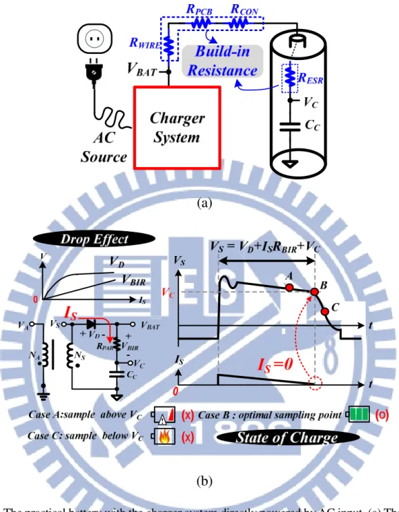
2.1 The Non-Ideal Effect of Practical Battery
As illustrated in Fig. 8(a), the charger system directly connected to the AC power supply charges the battery by the secondary-side discharging current IS through an electrical isolation which is composed of a transformer. RESR and CC are equivalent series resistance and capacitance existing in a practical battery, respectively. Parasitic resistance along the path from the charger system to the battery includes contact resistance RCON, wire resistance RWIRE, and printed circuit board (PCB) resistance RPCB. VBAT indicates the output node of the charger system. In contrast, the real battery voltage is denoted by VC as shown in Fig. 8. The foregoing parasitic elements cause non-ideal effect as shown in (1), and can be simplified as (2), where RBIR is short for build-in-resistance representing the total parasitic resistance along the charging path between charger and device.
(
)
BAT S ESR PCB WIRE CON C
V
=
I
×
R
+
R
+
R
+
R
+
V
(1)(
)
BAT S BIR C
V
=
I
×
R
+
V
(2)The charger system sees the value of VBAT rather than the real battery voltage VC The whole charging process will be affected due to the voltage difference between VBAT and VC. That is to say, built-in resistance (BIR) in Li-Ion battery charger systems should be carefully
solved for accurate and safety charging [10]-[14]. As we know, the battery cannot keep healthy and the device tends to be crashed or collapsed if the BIR can’t be alleviated
Not only the BIR but also the non-ideal diode will influence the voltage accuracy as depicted in Fig. 8(b), and the overall influence is called drop effect. The forward voltage of diode, VD, is a function of the secondary-side discharging current IS and can be expressed as VD(IS). That is, VD(IS) varies with IS during every single discharging period. VS and VA are the secondary-side and auxiliary-side voltages, respectively. The relationship between VS and VA can be expressed as (3) where NS and NA are the winding turn ratios of secondary and auxiliary sides, respectively.
( )
, where
=
A A S S D S S BIR C SN
V
V
V
V
I
I R
V
N
=
⋅
+
+
(3)The proposed trans-predictor technique can derive an accurate battery voltage from the auxiliary-side voltage VA because VA contains the real battery voltage information VC. However, the equation (3) includes the non-ideal drop effect caused by the discharging current IS. That is to say, the secondary-side discharging current IS will decrease the charging accuracy.
(a)
(b)
Fig. 8. The practical battery with the charger system directly powered by AC input. (a) The real battery compositions and the BIR effect along with the charging path. (b) The causal relationship between drop effect and state of charge (SOC).
2.2 The Principle of the Proposed Charger System
with Trans-Predictor
Fortunately, the drop effect can be eliminated when IS falls just to zero as shown on the right side of Fig. 8(b). When the system starts to discharge, the secondary voltage VS begins to ramp down until the discharging current diminishes to just zero. At the zero-current moment, the real battery voltage VC can be precisely extracted as noted by point B. The equation (3) can thereby exclude any non-ideal drop effect manifesting VS is completely equal to VC.
However, if the extracted point of VS is not the zero-current moment, it will have a great impact on the battery life time and further affect the safety problem. State of charge (SOC) corresponding to relative positions of extracted points, which makes big difference. That is, if the extracted point is above VC, battery would never be fully charged because the drop effect still influences the end voltage judgment in the charger system. On the other hand, if the extracted point is below VC, the charger system would think the battery has not been fully charged yet, and battery probably crashes or collapses because of all-the-time overcharging status. In summary, the importance of optimal extracted voltage VC can be obviously observed. Thanks to the help of trans-predictor, precisely detect the real battery voltage without any type of feedback network in charger system.
2.3 The Basic Operation of Flyback-based Controller
in Charger System
The architecture of flyback-based electrical isolation charger system with the proposed trans-predictor is illustrated in Fig. 9. The charger system is directly connected to the AC source, and the use of a transformer provides not only step-down output voltage VBAT, but also power supply VDDH to the charger controller. Thanks to the aid of the proposed trans-predictor, the charger system can work correctly without any type of feedback network.
Fig. 9. The architecture of flyback-based electrical isolation charger system with the proposed trans-predictor without any type of feedback network.
The trans-predictor utilizes VAUX derived in (4) to get the output voltage information. AUXB AUX A AUXA AUXB R V V R R = ⋅ + (4)
Substitution of (4) into (3), VC in (5), which contains non-ideal terms caused by the discharging current IS, is obtained.
[
( )
]
, where
S AUXA AUXB C TP AUX D S S BIR TP A AUXBN
R
R
V
k
V
V I
I
R
k
N
R
+
=
⋅
−
+
⋅
=
×
(5)To eliminate the non-ideal drop effect, the trans-predictor samples and holds the value of VAUX when the secondary-side discharging current IS falls to just zero. Therefore, non-ideal drop effects can be discarded in (5) and thus (6) can be derived without being affected by the secondary-side discharging current. In other words, the real battery voltage can be precisely designed because the constant k is known.
C T P A U X
V
=
k
⋅
V
(6)After the processing of the trans-predictor, the output voltage of error amplifier VER_V represents the output load situations without any physical feedback network and non-ideal effects as shown in (7). Therefore, the voltage loop is formed.
_ _ _
ER V ref V fb V
Consequently, high voltage accuracy can be obtained because the proposed trans-predictor excludes any non-ideal effects to fetch real battery voltage information VC with the advantage of electrical isolation as well. Besides, the removal of conventional feedback network further improves the area efficiency up to 11% of total PCB area to make the charger system as tiny as it could be. Moreover, the cost reduction can be achieved up to 5%.
The charger system with the proposed trans-predictor was fabricated in 0.5 µm 500V UHV process. Due to the 500V UHV process, the chip can be powered on directly by the AC source. After the power-on sequence, the supplying of the chip is controlled by the auxiliary windings rather than the AC source. That is, the chip works functionally.
2.3.1 The Operation of the Flyback System
The operation of flyback-based charger system is shortly explained in Fig. 10. In Fig. 10(a), IP, IS, and IVDDH are primary side charging current, secondary side discharging current, and power supplying current to the controller, respectively. There are three timing slots in one switching cycle, that is, the charging period Ton, discharging period TDIS and the resonant period TRE, respectively. In the charging status, the charging current IP flows through RCS to ground and generate VCS signal to feedback the input current information to the controller. In
the discharging status, VS is mainly affected by the drop effect because discharging current IS flows through diode D1 to deliver energy to battery. Simultaneously, the auxiliary side windings provide the power source VDDH to the controller. Besides, VS is in proportional to VA, the auxiliary side not only provides power source to the controller as it did originally, but also feeds the output information VAUX back to controller. In the resonant status, VS and VA start resonating because the input power has nowhere to go. The primary side NP and the parasitic capacitance of power MOSFET form the LC tank and thereby the resonant phenomenon is induced. In Fig. 10(b), when the charger system enters into TDIS, the secondary side starts to discharge energy to the battery. The drop effect continuously affects the detection of the battery voltage until the discharging current is just equal to zero. Therefore, an optimum VC point exists when the IS is equal to just zero since all non-ideal effects can be ignored. Sampling and holding the VC can accurately detect the battery voltage. Therefore, the charger system can detect the real battery voltage through the detection of VC at the point where the IS is equal to zero. In other words, at the junction between the two transitions of foregoing effects is the real battery voltage VC.
(a)
(b)
(c)
(d)
Fig. 10. The principle of the flyback-based charger system and the phenomena. (a) Charging period. (b) Discharging period. (c) Resonant period. (d) The drop effect and the resonant effect.
2.3.2 The Output Current Calculation
In addition, VS is in proportional to VA. IP,PK, IS,PK and VD indicate the peak current of the charging current, discharging current and the forward voltage of diode, respectively
In order to estimate the average output current, the current sensing information is sent by the VCS. Beside, charging current IP and discharging peak current IS,PK are obtained in (8), where NP/NS is winding turns ratio of primary and secondary side. Thus, the average output current IO,avg is derived in (9). Substitution of (8) into (9), IO,avg is obtained in (10) with three unknown variables. It’s recommended that switching period TS is kept constant. In other words, CC mode is operated with fixed switching frequency. As to the rest of the variables in (10), the system has to generate the relation that VCS,PK is reciprocal to TDIS. That is to say, if the equation (11) holds, the system is guaranteed to operate in a fixed average output current.
, , , CS P P S PK P PK CS S V N I I I R N = = × (8) , ,
1
(
)
2
S PK TDIS S avg SI
V
I
T
×
=
×
(9) , , 1 ( ) 2 CS PK P TDIS CS S S avg S V N V R N I T × × = × (10),
, where n is constant
CS PK TDISV
×
V
=
n
(11)2.3.3 The Constant Current Loop, Constant Voltage
Loop and Switching Frequency
For the charger system design, the constant current (CC) mode with a rated output current 1A and the constant voltage (CV) mode for battery voltage regulation are both needed [3], [10]. The system uses the CC mode to fast charge the battery by a large charging current for shrinking charging time when the output voltage is lower than VBAT. In contrast, the CV mode is selected to charge via smaller output current for ensuring a regulated and stable battery voltage. As illustrated in Fig. 11, the charger system operates at a fixed switching frequency when the CC mode is selected. However, the dynamic frequency is adopted in the CV mode to reduce switching power loss for enhancing efficiency at light loads. When the battery is nearly full to some extent, the system enters into deep green (DG) mode. The operating frequency is at most 50kHz in the CC mode and linearly decreases during the CV mode to reduce switching power loss. Finally it reaches the minimum 2kHz switching frequency to avoid any needless switching power loss. Thus, the efficiency can be kept at light loads.
Fig. 11. An overview of the charger system in terms of operating mode and switching frequency from battery low to battery high.
Thanks to the flyback-based converter characteristic, the trans-predictor can inherently exclude the non-ideal drop effect when the discharging current is just equal to zero, and the real voltage VC which excludes the non-ideal effects is extracted. Due to the aid of trans-predictor and the built-in 500V UHV process, the charger system can be directly connected to AC input to get activated with high voltage accuracy. Without any type of feedback network, the charger system can save as much as 30mm2, i.e., around 11% of PCB area. Besides, 5 % cost reduction can be achieved.
Chapter 3
The Circuit Implementations
In this chapter, the circuit implementations including trans-predictor, current-trans runner, input power protections, and other protection mechanism will be illustrated and explained with corresponding conceptual wave view, respectively. Due to the high voltage input environment, high voltage process should be used. The chip is fabricated in 0.5µm 500V UHV process.
3.1 The Trans-Predictor Circuit
As illustrated in Fig. 12(a), the circuit implementations of the proposed trans-predictor technique and the timing diagram of its operation. VAUX signal delivered by the auxiliary windings is processed to generate a delay signal, VPSE. Ton and Toff are on-time and off-time periods in one switching cycle, respectively (assume TRE is zero because the first valley of the resonant effect is picked). The detection signal, VSUB, the difference between VAUX and VPSE, can be used to tell the trans-predictor when to sample exact VC for high accuracy. VVG, setting as a virtual ground with a fixed relative reference DC value, is used to compare with VSUB to predict the battery voltage. VVG has the same DC value with VSUB when neither VAUX nor VPSE
is generated. As illustrated in Fig. 12(b), as long as the output current stops discharging, i.e., the discharging current is just equal to zero, sharp slope occurs at VAUX. Consequently, the drastic change at the VSUB, VPSE-VAUX, makes the trans-predictor trigger the sampling signal, VSH, which means the output information is caught and Vfb_V is sent to the controller concurrently. At the same moment, the VTDIS signal which is essentially useful in CC mode operation is obtained. That is, accurate battery voltage VC can be extracted. The trans-predictor not only keeps the electrical isolation characteristic, also help to fetch output information with high accuracy in an open-loop control.
(a)
(b)
Fig. 12. The circuit implementations of (a) the proposed trans-predictor technique and (b) the timing diagram of its operation.
3.2 The Current Trans-Runner Circuit
In an isolated structure, the output current information can’t be straightly obtained. Therefore, it is analytically to use equation (10) to estimate the output current information. It is mentioned before that the system needs to operate in fixed frequency under CC mode to guarantee the average output current maintains at fixed value. Therefore, it is desirable to create the relations between VCS,PK and VTDIS as shown in (11). As illustrated in Fig. 7, the circuit implementations of the current trans-runner and the timing diagram of its operation. VTDIS represents the discharging time and can be obtained from the trans-predictor circuit. The peak value of current sensing VCS can be transferred to Vfb_C which sends to error amplifier to generate VER_C. Therefore, the equation (12) holds.
_ 1 2 CS TDIS fb C V V V R C = × (12)
Substitution of (11) and (12) into (10), the equation (13) can be obtained, which manifesting the constant current can be guaranteed because all the elements in (13) are known. , 1 2 _
1
1
=constant
2
P S avg fb C S CS SN
I
R
C
V
T
R
N
=
×
×
×
×
×
×
(13)(a)
(b)
Fig. 13. The circuit implementations of (a) the circuit implementation of current trans-runner and (b) the timing diagram of its operation.
3.3 The Loop Selector
In order to guarantee the smooth transitions between CC mode and CV mode, the loop selector as depicted in Fig. 14 is designed in the proposed charger system. VER, the output of the loop selector, decides the dominance of either CC loop or CV loop in (12).
_ _
min( , )
ER ER V ER C
V = V V (14)
With the help of the loop selector, the transition between CC loop and CV loop is rather smooth. There is no perturbation form the transition result in VER signal. Therefore, the system stability can be guaranteed when the switch of modes occurs.
3.4 The Protection Mechanisms
As illustrated in Fig. 15, the protection mechanisms include the over power supply VDDH protection, over voltage protection (OVP) about the output voltage VBAT, and over current protection (OCP) about charging current are shown. VDDH and VCS are both coming from outside of the controller. That is, the controller exposed itself to high voltage environment. Once either of the two signals exceed their limit value VPS and VLMT, respectively, VPT will trigger to shut down power MOS to protect system from burning down. In addition, Vfb_V is used to protect system from output over voltage. Once the Vfb_V exceeds VOVP, VPT also triggers to protect the system.
3.5 The Power Compensation
As mentioned before, the charger system is directly connected to the power source via plugs and sockets. Consequently, the protection mechanisms are inevitable and indispensable in the circuit design for safety. Besides, because the charger system is made to be adaptive to universal input, the input AC power source ranges from 90V to as high as 264V. Therefore, the input power protection should be adaptive also. VIN and IIN is the direct current (DC) input voltage of the alternating current (AC) source and input current, respectively. Assume the maximum input power equals to constant and equation (15) can be obtained. VIN is inversely proportional to IIN. Therefore, the IIN limit should change according to VIN.
,max ,max
constant
IN IN IN
P
=
V
×
I
=
(15)As illustrated in Fig. 16(a), VLMT is adaptive input power limit. If the maximum input power remains unchanged, VLMT decreases linearly as VAC increases. As illustrated in Fig 16(b), the input power information IAUX changes along with VAUX during the charging state. The higher the VAC is, the more the IAUX and the lower the VLMT voltages are. Therefore, the charger system is able to adaptive to a universal input voltage range.
(a)
(b)
Fig. 16. The adaptive input power limit protection for universal input range. (a) The adaptive input power limit selection. (b) The circuit implementation of power compensation.
Chapter 4
System Stability Analysis
The proposed charger system supports universal plug and play (uPnP) for the mainstream portable devices. Therefore, the frequency response analysis is supposed to put into discussion separately. That is, the charger with battery and the charger without battery respectively. On the other side, the open-loop controller is composed of CC mode and CV mode according to the load situations. Consequently, the frequency response analysis of each mode is not the same. In the CV mode, the closed loop is formed only at the very moment where the discharging current is just to zero and the voltage information is caught simultaneously. In other words, the stability analysis can be discussed in that split second. However, in another aspect, the output current in CC mode is processed through current trans-runner to estimate and calculate the averaged output current. That is to say, the output current information does not feedback over to controller straight. The controller indirectly modulates the output current by estimation. As a result, the frequency response analysis in CC mode can be ignored due to the open-loop control method.
As illustrated in Fig. 17(a), an equivalent small signal model based on the architecture of the charger system in CV mode without battery is shown in Fig. 3 (a). The equivalent small
signal model incorporates control-to-output transfer function GCO with output-to-control transfer function GOC [15]-[19]. As depicted in Fig. 17 (b), the GOC contains parameter of trans-predictor and compensation network GC which is contributed by CCP, RCP and ROUT. ROUT is the output impendence of the error amplifier. The output voltage VBAT is the product of the averaged output current IS,avg and the output impedance ZO which contains Cout and the dummy load RDM.
(a)
(b)
Fig. 17. The small signal model with (a) the block diagram and (b) the compensation network.
As derived in (9), the equation can be transformed into (16), where f(VER_V) represents the switching frequency.
, ,
(
)
(
_)
2
DIS S PK S avg ER VT
I
I
=
×
×
f V
(16)From Fig. 5, the switching frequency decreases linearly when the battery is from low to full. Therefore, the switching frequency f(VER_V), the reciprocal of the switching time and a function of VER_V, can be approximated to a linear function in (17), where K and C are constant. That is, the switching frequency is controlled by the error signal VER_V in the CV mode.
_ _
(
ER V)
ER Vf V
=
K V
×
+
C
(17)As depicted in Fig. 18, one switching cycle period can be divided to three timing slots Ton, TDIS and TRE. Ton and TDIS can be obtained by the slopes of the charging and discharging current. Besides, the slopes can be estimated by the components employed in the system. Ton, TDIS and IS,PK can be obtained in (18) to (20), respectively where Lp is the inductance of the primary side windings.
_
1
p on ER V IN CSL
T
V
V
R
=
×
×
(18)2 ,
(
)
p S DIS S PK BAT PL
N
T
I
V
N
=
×
×
(19) , IN P S PK on p SV
N
I
T
L
N
=
×
×
(20) IN CS p V R L ⋅ 2 1 BAT p V N L × −Fig. 18. The analytical wave view in one switching cycle.
Substitution of equations (18) to (20) into (16), IS,avg can be expressed in (21).
(
3 2)
_ _ , 22
ER V ER V p S avg BAT CSK V
C V
L
I
V
R
×
+
×
×
=
×
×
(21)In order to obtain the small signal analysis, linearization at the quiescent operating point can be derived (22). Then, the small ac current variation at the secondary side flowing through the impedance ZO determines the perturbation of VBAT as expressed in (23).
, 1 _ 2 ˆ ˆ ˆ S a v g E R V B A T I = a ⋅V + a ⋅V , 2 , _ _ 1 2 _ 3 2 , _ _ 2 2 2
(3
+2
)
2
-(
)
2
S avg ER V ER V p ER V BAT CS S avg ER V ER V p BAT BAT CSI
K V
CV
L
a
V
V
R
I
KV
CV
L
a
V
V
R
∂
×
×
=
=
∂
×
×
∂
+
×
=
=
∂
×
×
(22) , 1 _ 2 ˆ ˆ ( ˆ ˆ ) B A T S a v g O E R V B A T O V = I × Z = a ×V + a ×V × Z (23)Therefore, the control-to-output transfer function GCO(s) is depicted in (24), which simply contains one load-dependent pole ωP0.
1 1 2 2 _ 2
ˆ
1
ˆ
1-
1
-1
1
-O BAT CO out O DM ER V DMZ
a
V
a
G
s C
Z
a
R
a
V
R
a
×
=
=
=
×
×
×
+
(24)On the other hand, the output-to-control transfer function GOC(S) can be derived in (25), where the transconductance of error amplifier EA in Fig. 11 (b) is gm. Hence, the transfer function GOC(s) contains one pole ωP1 and one zero ωZ1.
_
ˆ
1
( )
ˆ
1
ER V m OUT CP CP OC TP OUT CP BATV
g R
sR C
G
s
K
sR
C
V
+
=
=
×
+
(25)Without battery, the compensation pole ωP1 is set to be the system dominant pole in proposed charger system. In addition, the zero ωZ1 is designed to cancel the load-dependent pole ωP0 of GCO(s). After the compensation, the system bandwidth is designed at about 1kHz which is far away from the switching frequency and the system transfer function T(s) is shown in (26). 1 2 ( ) ( ) ( ) 1 1 1 1 where 1 / CO OC m OUT CP CP out TP OUT CP DM T s G s G s g R sR C a s C m K sR C m m R a = × + = × × × × + + = − (26)
As depicted in Fig. 19, the bode plot of the proposed charger system is presented. If the charger is without battery, the dominant pole is ωP1 and ωZ1 has to be designed at the place where ωP0 appears at the lightest load condition. On the other hand, if the system is battery-connected, the dominant pole is decided by the equivalent capacitance of the battery itself. As a result, the system becomes a one-pole system.
Chapter 5
Experimental Results
In this chapter, the design specifications are shown in section 5.1. The chip micrograph and PCB prototype are presented in section 5.2.
5.1 Design Specifications Chip Micrograph and PCB
Prototype
The proposed flyback-based charger system with trans-predictor and current trans-runner was fabricated in 0.5µm 500V ultra-high voltage (UHV) process. The chip micrograph with an active area of 4.75mm2 is shown in Fig. 20(a) and the prototype with the dimensions of 45mm by 40mm is shown in Fig. 20(b). The efficiency of the experimental results is in Fig. 21. Due to the GM mode, the efficiency can achieve 85% and 80% in light load condition at 90VAC and 264VAC, respectively. The peak efficiency is 93.1% under the
HV Startup UVLO Pre - Regulator Trans-Predictor Current Runner HV-Driver PWM ZCD 2500µm
(a)
(b)
Fig. 20. (a) Chip micrograph. (b) Prototype.
Fig. 21. The efficiency of the experimental results in charger system.
The input AC source from 90 to 264VAC and the rated output voltage VBAT is 4.2V. The primary side, secondary side and auxiliary side inductance of transformer are 700µH, 4.86µH,
and 49.7µH, respectively. That is, the winding turns ratio Np: Ns: Na is 12T: 1T: 3T. Design specifications are listed in Table I in more details.
Table II: Design specifications
Technology
0.5µm 500V UHV
Input Line Voltage Range (V
rms)
90~264
Output Voltage (V)
4.2
Output Power (W)
4.2
Constant current output (A)
1
Switching Frequency (Hz)
2K-50KHz
Maximum Efficiency (%)
90.2@V
AC=264V
Chip Area (µm
2)
1900 × 2500
Table III : Comparison table
This work
[3]
[4]
[5]
Technology
0.5µm
0.5µm
0.5µm
0.5µm
Input Voltage(V)
AC 90-264
DC 3-4.3
DC 60
DC 10
External Feedback
NO
Resistor
Divider
Resistor
Divider
Resistor
Divider
Electrical Isolation
YES
NO
NO
NO
Output Voltage Range (V)
2.7-6
4.2
4.2-58.8
2.1-4.2
Voltage Accuracy (%)
99.65
99.57
NA
NA
Switching Frequency(Hz)
2K-50K
NA
NA
2.2M
Efficiency (%)
93.1
90
92
86
Chip Area (mm
2)
4.75
NA
0.37
1.6
5.2 Experimental Results
Experimental results are as follows. Input voltage is AC 110rms. In Fig. 22, the switching period can be divided into Ton, TDIS and TRE as shown. When the period Ton starts, the current sensing VCS begins to increase. On the other hand, the system starts to resonate after TDIS ends at zero current of IS. VDRAIN, the drain terminal of the power MOS, reflects the secondary voltage VS to as high as hundreds voltage. Therefore, the VIS 500 UHV fabrication is adopted. The switching period can be divided into Ton, TDIS and TRE as shown. When the period Ton starts, the current sensing VCS begins to increase. On the other hand, the system starts to resonate after TDIS ends at zero current of IS.
As shown in Fig. 23(a), the output VBAT is the rated voltage 4.2V. VFB is proportional to VBAT all the time and VBAT is pretty close to the rated voltage, 4.2V within ± 0.35% variations under all kinds of situations. In Fig. 23(b), the drop effect and resonant phenomenon can be apparently observed during every off-time period. That is, the VAUX signal is with a ramped slope before IS decreases to zero. Then, an extremely sharp slope occurs right after the zero-current point happens. The accuracy of the battery voltage can be guaranteed because the proposed trans-predictor is to sample and hold the VC when the discharging current is right down to zero in every single cycle. Therefore, the VFB tightly attaches to the same value of the VAUX where the discharging current is down to zero owing to the operation of the
trans-predictor. That means the trans-predictor is capable of capturing the real battery voltage VC without any disturbance of the drop effect or influence from resonant phenomenon.
As shown in Fig. 24, the different loading conditions are shown and the VSH represents the sampling signal. In Fig. 24(a), the system can precisely capture the zero-current point of VAUX which represents the real battery voltage VC without any non-ideal effect at 500mA loading. Under the same test bench except the loading change to 1000mA, the TRE shrinks a lot, which means the average output current is raised. The result shows that the proposed trans-predictor can sample and hold at the zero-current point of VAUX no matter the change of the output current IS.
(b)
(a)
(b)
Fig. 23.The measurement results. (a) The charger system from battery low to battery high. (b) The BIR effect and resonant phenomenon.
(a)
(b)
Fig. 24. The measurement results at different conditions of load. (a) The charger system at 500mA loading. (b) The charger system at 1000mA loading.
As shown in Fig 25, the constant current is obtained at 1A as long as the output voltage is less than the target voltage. The switching frequency is always the same when the
charger is operating under CC mode. Therefore, the proposed charger can correctly operate under CC mode.
(a)
(b)
Fig. 25.The measurement results of constant current mode. (a) The output voltage is 3V. (b) The output voltage is 4V.
As shown in Fig. 26, the measurement results of accuracy variation is presented. After a large amount of measuring samples, the result shows that the real battery voltage is pretty
near to value Vfb_V sampled and hold by the proposed trans-predictor circuit. The variation is within ± 0.35%.
Fig. 26.The measurement results of accuracy variation.
The comparison between the proposed trans-predictor charger system converter and prior arts is listed in Table II. The proposed charger system can directly connect to AC power source because of the built-in UHV power MOSFET. Besides, the proposed trans-predictor technique provides high accuracy of battery voltage regulation without any type of feedback network.
Chapter 6
Conclusions and Future Works
6.1 Conclusions
The test chip was fabricated in VIS 0.5µm 500V UHV Process. Owing to the 500V ultra-high voltage device, the chip can be powered on directly by the AC source. After the power-on sequence, the supplying of the chip is controlled by the auxiliary windings and the function of the trans-predictor can work correctly. 99.65% of the voltage accuracy is achieved by the proposed trans-predictor in electrical isolation charger applications. The proposed trans-predictor enhances area efficiency and cost advantage by 11% and 5%, respectively. In contrast, conventional feedback network occupies at least 30mm2.
6.2 Future Works
This thesis proposed a technique to realize the isolated charger with high voltage accuracy and excludes all the non-ideal effects. However, the constant current regulation is still operating in constant frequency. It will make the efficiency poorer than CV regulation duo to the constant switching frequency. How to remain in constant current with dynamic frequency becomes an interesting topic.
References
[1] S. Dearborn, "Charging Li-ion batteries for maximum run times," Power Electronics Technology Magazine, pp. 40–49, Apr. 2005.
[2] Y.-H. Liu, C.-H. Hsieh, and Y.-F. Luo, "Search for an optimal five-step charging pattern for Li-Ion batteries using consecutive orthogonal arrays," IEEE Trans. on Energy Convers., vol.26, no.2, pp.654-661, Jun. 2011.
[3] M. Chen and G. A. Rincón-Mora, "Accurate, compact, and power-efficient Li-ion battery charger circuit, " IEEE Trans. Circuits Syst. II, Exp. Briefs, vol. 53, no. 11, pp. 1180–1184, Nov. 2006.
[4] C.-L. Chen and K.-H.Chen, "800V ultra-high-voltage start-up mechanism for pre-regulator in power factor correction (PFC) controller," in Proc. IEEE MWSCAS, pp. 1-4 Aug. 2011. [5] X. Zhang, H. Liu, and D. Xu, "Analysis and design of the flyback transformer," in Proc.
IEEE IECON, pp. 715-719, Nov. 2003.
[6] K.B. Park, C.E. Kim, G.W. Moon; M.J. Youn, “PWM Resonant Single-Switch Isolated Converter,” IEEE Trans. Power Electron., vol.24, no.8, pp.1876-1886, Aug. 2009
[7] Torrico-Bascop R., Barbi N., “A double ZVS-PWM active-clamping forward converter: analysis, design, and experimentation,” IEEE Trans. Power Electron., vol.16, no.6, pp.745-751, Nov. 2001
[8] S.-H. Yang, J.-W. Liu, and C.-C. Wang, "A single-chip 60-V bulk charger for series Li-Ion batteries with smooth charge-mode transition," IEEE Trans. on Circuits and Syst. I, pp.1588 - 1597, Jul. 2012.
[9] R. Pagano, M. Baker, and Radke, R.E., "A 0.18-µm monolithic Li-Ion battery charger for wireless devices based on partial current sensing and adaptive reference voltage," IEEE J. of Solid-State Circuits, vol.47, no.6, pp.1355,1368, Jun. 2012.
[10] C.-H. Lin, C-Y. Hsieh, K.-H Chen, "A Li-Ion Battery Charger with Smooth Control Circuit and Built-In Resistance Compensator for Achieving Stable and Fast Charging," IEEE Trans. on Circuits and Syst. I, Reg. papers, vol. 57, no 2, Feb. 2010.
[11] C.-H. Lin, C.-L. Chen, Y.-H. Lee, S.-J. Wang, C.-Y. Hsieh, H.-W. Huang, K.-H. Chen, "Fast Charging Technique for Li-Ion Battery Charger," IEEE International Conf. on Electronics, Circuits and Syst., pp. 618-621, Sep. 2008.
[12] C.-H. Lin, H.-W. Huang K.-H. Chen, "Built-in Resistance Compensation Technique for Fast Charging Li-Ion Battery Charger," IEEE Custom Integrated Circuits Conf., pp. 33-36, Sept 2008.
[13] S.-P. Roland, "A Dynamic Voltage-Compensation Technique for Reducing Charge Time in Lithium-Ion Batteries," The 15th Annual Battery Conf. on Applications and Advances, pp. 179-184, Jan. 2000.
[14] J. Buxton, "Li-Ion battery charging requires accurate voltage sensing," Anal. Devices Anal. Dialog., vol. 31, no. 2, 1997.
[15] Irving, B.T., Panov Y., Jovanovic M.M., "Small-signal model of variable-frequency flyback converter," in Proc. IEEE APEC’03, 2003, pp.977–982., vol.2, pp.977-982, Feb. 2003. [16] Panov Y., Jovanovic M.M., "Small-signal analysis and control design of isolated power
supplies with optocoupler feedback," IEEE Trans. Power Electron., vol.20, no.4, pp. 823- 832, July 2005.
[17] Suntio T., "Average and small-signal modeling of self-oscillating flyback converter with applied switching delay," IEEE Trans. Power Electron., vol.21, no.2, pp. 479- 486, Mar. 2006.
[18] Christophe Basso, "Understanding Loop Compensation with Monolithic Switchers" ON Semiconductor, Application Note, AND8334/D.
[19] Jee-Hoon Jung, "Feed-Forward Compensator of Operating Frequency for APWM HB Flyback Converter," IEEE Trans. Power Electron., vol.27, no.1, pp.211-223, Jan. 2012.