This content has been downloaded from IOPscience. Please scroll down to see the full text.
Download details:
IP Address: 140.113.38.11
This content was downloaded on 26/04/2014 at 03:41
Please note that terms and conditions apply.
Fabrication of InGaN/GaN nanorod light-emitting diodes with self-assembled Ni metal islands
View the table of contents for this issue, or go to the journal homepage for more
2007 Nanotechnology 18 445201
(http://iopscience.iop.org/0957-4484/18/44/445201)
Nanotechnology 18 (2007) 445201 (4pp) doi:10.1088/0957-4484/18/44/445201
Fabrication of InGaN/GaN nanorod
light-emitting diodes with self-assembled
Ni metal islands
C H Chiu
1, T C Lu
1, H W Huang
1, C F Lai
1, C C Kao
1, J T Chu
1,
C C Yu
1, H C Kuo
1,4, S C Wang
1, C F Lin
2and T H Hsueh
31Department of Photonics, National Chiao Tung University, Hsinchu 300, Taiwan,
Republic of China
2Department of Materials Engineering, National Chung Hsing University, Taichung 400,
Taiwan, Republic of China
3Institute of Electro-Optical Science and Engineering, Center for Micro/Nano Science and
Technology, National Cheng Kung University, Tainan 70101, Taiwan E-mail:[email protected]
Received 31 May 2007, in final form 4 September 2007
Published 9 October 2007
Online at
stacks.iop.org/Nano/18/445201
Abstract
We report the fabrication of InGaN/GaN nanorod light-emitting diodes
(LEDs) using inductively coupled plasma reactive-ion etching (ICP-RIE) and
a photo-enhanced chemical (PEC) wet oxidation process via self-assembled
Ni nanomasks. An enhancement by a factor of six times in
photoluminescence (PL) intensities of nanorods made with the PEC process
was achieved in comparison to that of the as-grown structure. The peak
wavelength observed from PL measurement showed a blue shift of 3.8 nm for
the nanorods made without the PEC oxidation process and 8.6 nm for the
nanorods made with the PEC oxidation process from that of the as-grown
LED sample. In addition, we have demonstrated electrically pumped nanorod
LEDs with the electroluminescence spectrum showing more efficiency and a
10.5 nm blue-shifted peak with respect to the as-grown LED sample.
(Some figures in this article are in colour only in the electronic version)
1. Introduction
Direct wide-bandgap gallium nitride (GaN) and other III-nitride-based semiconductors have attracted much attention for potential applications such as blue, green, and ultraviolet (UV) light-emitting diodes (LEDs) and blue laser diodes [1]. Additionally, it has been widely proposed that fabricating nanostructures on the LEDs can enhance the performance effectively due to the quantum confinement and the strain-releasing effect [2]. For GaN-based nanoscale structures, so far, the GaN nanorods have been produced by various fabrication methods, such as growth of InGaN/GaN multiple quantum nanocolumns/nanorods on Si substrate by radio-frequency (RF) plasma-assisted molecular-beam epitaxy [3] or growth of single-crystal GaN nanorods by hybrid vapor-phase epitaxy [4], synthesis using carbon nanotubes as templates [5], inductively coupled plasma-reactive ion etching (ICP-RIE) 4 Author to whom any correspondence should be addressed.
without masks [6] or via e-beam patterned [7] nanorods, each with a relatively complicated process. To simplify the patterning process, it is possible to produce nanoscale self-assembled nickel (Ni) islands by choosing the correct Ni layer thickness, annealing time and annealing temperature on top of the LED surface [8]. Nevertheless, the rough unprotected sidewalls of multiple quantum wells (MQWs) embedded in nanorods etched by ICP-RIE could suffer from a large leakage current, resulting in poor electrical properties. In addition, nanorods fabricated via such methods are difficult to form into p-type ohmic contacts for each individual nanorod. Besides, the photo-enhanced chemical (PEC) wet oxidation process has been used in GaN-based LEDs to oxidize the exposed surface material for passivation and surface roughening to enhance the light output [9,10]. In this paper, we introduce a novel method combining ICP-RIE and the PEC wet oxidation process with self-assembled Ni metal islands to fabricate InGaN/GaN nanorod LEDs.
Nanotechnology 18 (2007) 445201 C H Chiu et al
2. Device fabrication
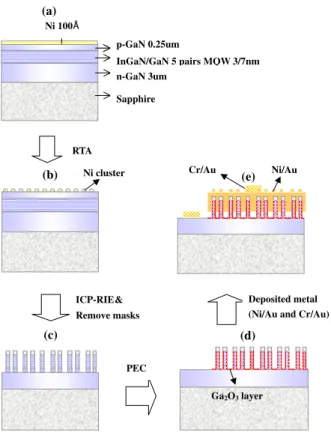
The process flowchart for making the nanorod LEDs with the PEC oxidation process is shown in figure1. The GaN-based LED samples were grown by metal-organic chemical vapor deposition (MOCVD) on a c-axis sapphire (0001) substrate; they consist of a 50 nm thick GaN nucleation buffer layer, a 3.0 µm thick highly conductive Si-doped GaN layer, five periods of 3/7 nm thick undoped In0.21Ga0.79N/GaN MQWs, a 50 nm thick Mg-doped AlGaN layer and finally a 0.25µm thick Mg-doped GaN layer. The LED samples were then taken to undergo the nanorod manufacturing process. First, a 100 ˚A Ni layer was deposited on top of the LED samples by an e-gun evaporator (figure1(a)). The Ni-coated LED samples were subsequently subjected to rapid temperature annealing (RTA) under flowing N2at 850◦C for 1 min to form self-assembled Ni metal clusters (figure 1(b)). Then, the LED samples were etched down to the n-type GaN layer by the ICP-RIE system (SAMCO ICP-RIE 101iPH) operated at 13.56 MHz under a gas mixture of Cl2/Ar = 50/20 sccm with 2 min of etching time to form nanorods. The ICP source power, bias power and the chamber pressure of the ICP-RIE system were set at 400/100 W. Then, the samples were dipped into a nitric acid solution (HNO3) at 100◦C for 5 min to remove the Ni nanomask (figure 1(c)) and this was followed by the PEC oxidation process. Details of the nanorod formation process were given in [11]. An 800 W Hg lamp was used as the illumination source in the PEC oxidation process in the unstirred deionized water. An external dc bias fixed at positive 20 V was applied to the n-type GaN layer surface as the anode contact and platinum was used as the cathode, with 10 min as the exposure time. The light power density of the Hg lamp was fixed at 2.5 W cm−2to illuminate the front side of the LED samples. Then, the Ga2O3layer was formed at the nanorod sidewall and the ICP-etched n-type GaN layer (figure1(d)). The p-type layer was nearly unoxidized due to its low conductivity [12]. Finally, a 20/500 nm thick Ni/Au layer was deposited on the entire surface of the PEC nanorod LED to form a connection with the p-type ohmic contacts for an individual nanorod. A 20/800 nm thick Cr/Au was then deposited as the p and n bonding electrodes (figure1(e)).
After all processes in the manufacture of the nanorod LEDs were done, the dimensions and density of the nanorod LED samples made with and without the PEC oxidation process were estimated by scanning electron microscopy (SEM), as shown in figure2. Figure2(a) shows that the size and density of the self-assembled Ni masks on the p-GaN surface of an LED sample were approximately 250 nm and 3×109cm−2. The InGaN/GaN MQW nanorod density was estimated to be approximately 3 ×109 cm−2. Figure 2(b) shows that the diameter and the etching depth of nanorods were about 140 nm and 0.5µm, respectively. Figure2(c) shows the InGaN/GaN MQW nanorod LED after the PEC process; the left-hand side shows the nanorods made with the PEC process and the right-hand side shows the ICP-RIE etching surface after the PEC process. The inset of figure2(c) framed with a dashed (red) line shows higher magnification of the nanorods after the PEC oxidation process. The composition elements of the nanorods before and after the PEC oxidation process have been identified by energy dispersive x-ray (EDX) spectral
(a) p-GaN 0.25um InGaN/GaN 5 pairs MQW 3/7nm Sapphire n-GaN 3um Ni 100Å RTA Ni/Au (e) Cr/Au (b) Ni cluster Deposited metal (Ni/Au and Cr/Au) ICP-RIE Remove masks (c) (d) Ga2O3 layer PEC &
Figure 1. Schematic illustration of InGaN/GaN MQW nanorod LED
process flowchart. (a) A thin Ni layer deposited on the LED surface. (b) Ni clusters were formed on surface after 850◦C RTA.
(c) ICP-RIE process to fabricate GaN nanorods followed by removal of the Ni clusters in heated HNO3. (d) An Ga2O3layer was formed
on the exposed surface by the PEC wet oxidation process. (e) Contact metal (Ni/Au) was deposited on the nanorods to form connections with p-type ohmic contacts.
analysis. The result shows only Ga and N elements in samples made without the PEC process, but a large amount of O was observed in samples made with the PEC oxidation process. This shows that a thin Ga2O3layer was formed with the PEC process. Comparing the nanorod structure in figures 2(b) and (c), the diameters of the nanorods made without and with the PEC oxidation process were about 140 nm and 155 nm, respectively. It also shows that the diameter of the nanorods reduced to about 90 nm after removing the Ga2O3 oxidation layer. Figure2(d) shows the Ni/Au contact metal deposited on InGaN/GaN MQW nanorods to form connections with the p-type ohmic contacts for each individual nanorod.
3. Results and discussion
Figure3shows the normalized PL spectrum of the as-grown LED sample, and nanorod LED samples made with and with-out the PEC process measured at room temperature. A HeCd laser (325 nm) was used with an excitation power of 25 mW and the power density of 1.5 W cm−2. The PL emission peaks of the InGaN/GaN active layer were ob-served at 449.0, 445.2 and 440.4 nm for as-grown sam-ples, and nanorods samples made without and with the PEC oxidation process, respectively. The PL peak intensities of InGaN/GaN MQW active layers in nanorods made with and without the PEC oxidation process were enhanced by 2
Figure 2. SEM images of (a) Ni nanomasks on the p-GaN top surface after the RTA process, (b) InGaN/GaN MQW nanorod LED after
ICP-RIE etching. (c) InGaN/GaN MQW nanorod LED after the PEC process. (d) InGaN/GaN MQW nanorod LED after deposition of the contact metal. 350 400 450 500 0.0 0.2 0.4 0.6 0.8 1.0 1.2 1.4
Normalized PL Intensity (a.u.)
Wavelength (nm)
as-grown LED
Nanorods LED without PEC Nanorods LED with PEC
449.0 nm 445.2 nm
440.4 nm x6
x1.2
Figure 3. Normalized PL intensity spectra for as-grown LED and
nanorod LEDs made with and without the PEC process at room temperature.
factors of approximately six and five times compared with as-grown LED samples. The blue-shift phenomena were ob-served for both the nanorod LED samples made with and without the PEC oxidation process, and the blue-shift values were 3.8 nm (20 meV) and 8.6 nm (50 meV), respectively. The blue shift might be caused by the partial reduction of the piezoelectric field by the strain release in the nanorod struc-tures [7, 10]. The blue-shift phenomenon of nanorods made with the PEC process was stronger than that made without the PEC process, due to the further reduced diameters. The peak shifts can be translated to the reduction of the piezo-electric field at around 20 meV/3 nm=66.7 kV cm−1 and 50 meV/3 nm=166.7 kV cm−1, for LED samples made with and without PEC oxidation process, respectively (where 3 nm is the well thickness). On the other hand, the PL enhancement
0 2000 4000 6000 8000 10000 12000 14000 16000 457.4 nm 467.9 nm
EL intensity ( arb. units)
Wavelength (nm)
nanorod LED with ECP as-grown LED
350 400 450 500 550
Figure 4. The EL intensity spectra for as-grown LED and nanorod
LED made with the PEC process at room temperature. The inset shows a photographic image of the blue emission from an InGaN/GaN MQW nanorod LED at 1 mA dc current.
could result from the sidewall scattering in the nanorod struc-tures [2, 11]. In addition, the enhancement of the PL inten-sity could be explained by the increased wavefunction overlap of the electron and the hole band structure of the InGaN/GaN MQWs with the partially reduced piezoelectric field. One can see that the nanorods made with the PEC oxidation process have a higher PL intensity and a larger piezoelectric reduction due to the smaller nanorod diameters in the samples made by the PEC oxidation process. This shows that the PEC oxidation process not only can form an oxidation layer to isolate the in-dividual nanorod electrically, but also reduces the diameter of the nanorods to cause a stronger strain-relaxation effect [7,10]. Figure 4 shows the room-temperature EL spectrum of the as-grown LED and nanorod LED samples made with the PEC oxidation process at an injection current of 1 mA. The
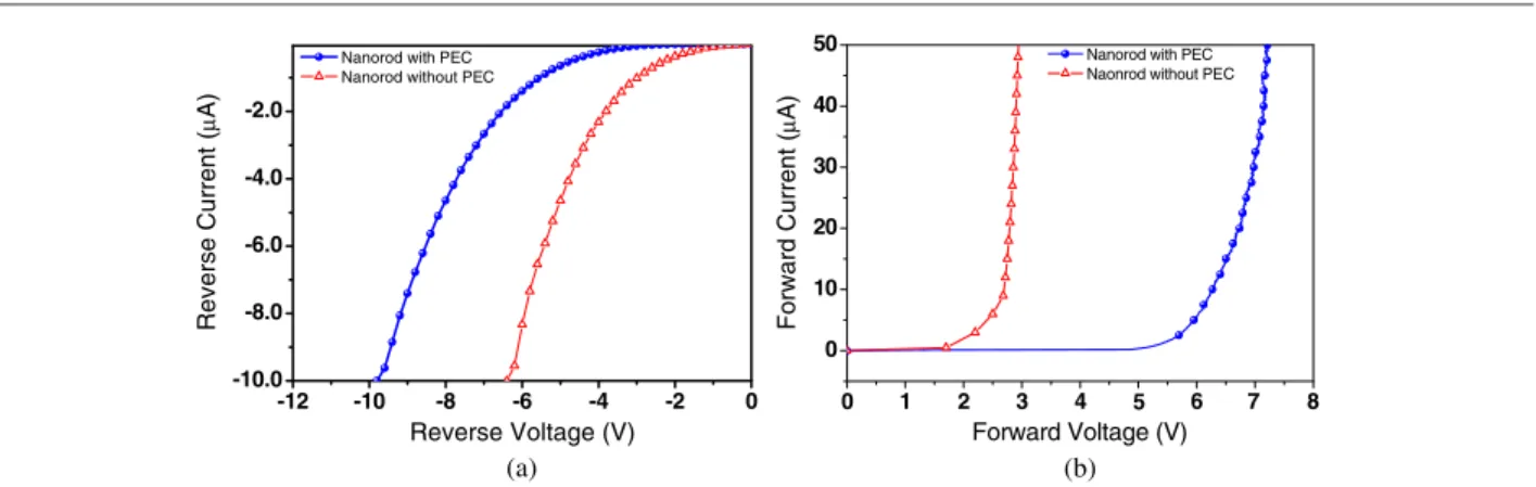
Nanotechnology 18 (2007) 445201 C H Chiu et al 0 5 6 7 8 10 20 30 40 50 0 1 2 3 4 Forward Voltage (V) Forward Current ( µ A)
Nanorod with PEC Naonrod without PEC
-12 -10 -8 -6 -4 -2 0 -10.0 -8.0 -6.0 -4.0 -2.0 Reverse Current ( µ A) Reverse Voltage (V)
Nanorod with PEC Nanorod without PEC
(a) (b)
Figure 5. (a) The reverse-bias and (b) forward-bias current–voltage characteristics of nanorods made with and without the PEC oxidation
process.
inset of figure4shows the emission image of the InGaN/GaN MQW nanorod LED. It shows that the PEC oxidation process can effectively form oxidation layers to isolate the nanorods and facilitate contact formation. The EL intensity of the nanorod LED made with the PEC process was about 1.76 times that of the as-grown LED. The EL MQW emission peaks of the InGaN/GaN active layer were observed at 467.9 nm and 457.4 nm for as-grown samples and nanorod samples made with the PEC oxidation process, respectively. The blue-shift effect was again observed for the nanorod LED samples made with the PEC oxidation process, with a blue-shift value of 10.5 nm (60 meV), which was similar to the observation in the PL measurement.
The reverse-bias and forward-bias current–voltage charac-teristics of nanorods made with and without the PEC oxidation process were also measured, and they are shown in figures5(a) and (b). The reverse-bias leakage current in the nanorods made with the PEC oxidation process is significantly reduced com-pared to that in the nanorods made without the PEC oxidation process. This is due primarily to the fact that oxidation layers produced in the PEC oxidation process form excellent isola-tion layers to reduce the leakage current through the sidewalls of the nanorods. In addition, the forward-bias characteristics also show a difference in current level for the two types of nanorod LEDs. A higher turn-on voltage of the PEC-oxidized nanorod LED was clearly observed. Such high forward volt-age is probably due to the smaller contact area and the non-optimized ohmic contact metal conditions. The accompanying thermal effect also explained why the enhancement factor in the EL measurement result was smaller than that in PL result.
4. Summary
We fabricated InGaN/GaN nanorod LEDs using self-assembled Ni nanomasks, ICP-RIE etching and the PEC pro-cess. The PEC process produced Ga2O3oxidation layers sur-rounding the nanorods to provide a better isolation for the nanorods, and to bring p-type GaN nanorods in contact with p-type electrodes more easily. Enhancement by factors of six and five times in the PL intensities of nanorods made with and without the PEC process compared to that of as-grown struc-tures was observed. Also, the EL spectrum showed more ef-ficiency, and a 10.5 nm blue-shift peak of the nanorods made with the PEC process from that of the as-grown LED sample.
Acknowledgments
The work was supported by the MOE ATU program and in part by the National Science Council of the Republic of China (ROC) in Taiwan under Contract Nos NSC 95-2120-M-009-008, NSC 95-2752-E-009-007-PAE, and NSC 95-2221-E-009-282.
References
[1] Nakamura S, Senoh M, Nagahama S, Iwasa N, Yamada T, Matsushita T, Kiyoku H and Sugimoto Y 1996 InGaN-based multi-quantum-well-structure laser diodes Japan. J. Appl.
Phys.35 L74
[2] Hsueh T H, Huang H W, Kao C C, Chang Y H, Ou-Yang M C, Kuo H C and Wang S C 2005 Characterization of
InGaN/GaN multiple quantum well nanorods fabricated by plasma etching with self-assembled nickel metal nanomasks
Japan. J. Appl. Phys.44 2661
[3] Kikuchi A, Kawai M, Tada M and Kishino K 2004 InGaN/GaN multiple quantum disk nanocolumn light-emitting diodes grown on (111) Si substrate Japan. J. Appl. Phys.43 L1524
[4] Kim H M, Kim D S, Kang T W, Cho Y H and Chung K S 2002 Growth and characterization of single-crystal GaN nanorods by hydride vapor phase epitaxy Appl. Phys. Lett.81 2193
[5] Han W Q, Fan S S, Li Q Q and Hu Y D 1997 Synthesis of gallium nitride nanorods through a carbon
nanotube-confined reaction Science277 1287
[6] Yu C C, Chu C F, Tsai J Y, Huang H W, Hsueh T H, Lin C F and Wang S C 2002 Gallium nitride nanorods fabricated by inductively coupled plasma reactive ion etching Japan. J.
Appl. Phys.41 L910
[7] Chen H S, Yeh D M, Lu Y C, Chen C Y, Huang C F, Tang T Y, Yang C C, Wu C S and Chen C D 2006 Strain relaxation and quantum confinement in InGaN/GaN nanoposts
Nanotechnology17 1454
[8] Carey J D, Ong L L and Silva S R P 2003 Formation of low-temperature self-organized nanoscale nickel metal islands Nanotechnology14 1223
[9] Chen L C and Huang Y L 2004 High reliability GaN-based light-emitting diodes with photo-enhanced wet etching Solid
State Electron.48 1239
[10] Lin C F, Zheng J H, Yang Z J, Dai J J, Lin D Y, Chang C Y, Lai Z X and Hong C S 2006 High-efficiency InGaN-based light-emitting diodes with nanoporous GaN:Mg structure
Appl. Phys. Lett.88 083121
[11] Huang H W, Chu J T, Hsueh T H, Ou-Yang M C, Kuo H C and Wang S C 2006 Fabrication and photoluminescence of InGaN-based nanorods fabricated by plasma etching with nanoscale nickel metal islands J. Vac. Sci. Technol. B
24 1909
[12] Lin C F, Yang Z J, Zheng J H and Dai J J 2005 Enhanced light output in nitride-based light-emitting diodes by roughening the mesa sidewall Photon. Technol. Lett.17 2038