cuit realized with ESD clamp device drawn in the layout style of big field-effect transistor (BigFET), and with parasitic diode of BigFET as a part of ESD-transient detection mechanism, is proposed and verified in a 65-nm 1.2-V CMOS process. Skillfully utilizing the diode-connected MOS transistor as the equivalent large resistor and the parasitic reverse-biased diodes of BigFET as the equivalent capacitors, the new RC-based ESD-transient detection mechanism can be achieved without using an actual resistor and capacitor to significantly reduce the layout area by ∼82%, as compared to the traditional RC-based ESD-transient detection circuit. From the measured results, the new proposed power-rail ESD clamp circuit with body effect of ESD clamp device can perform adjustable holding voltage under the ESD stress condition, as well as better immunity against mistrigger and transient-induced latch-on under fast power-on and transient noise conditions.
Index Terms—Big field-effect transistor (BigFET), electrostatic discharge (ESD), power-rail ESD clamp circuit.
I. INTRODUCTION
I
N ADVANCED nanoscale CMOS technology, the electro-static discharge (ESD) clamp device drawn in the layout style of big field-effect transistor (BigFET) had demonstrated excellent ESD protection performance [1]–[6]. In these power-rail ESD clamp circuits, the ESD clamp devices can discharge a large ESD current by the inversion channel layer without snapback operation of the parasitic BJT [7]–[10]. Practically, there are two different circuit skills, namely, the RC-delay technique [1]–[3] and the capacitance-coupling design [4]–[6], to realize the ESD-transient detection circuit in the power-rail ESD clamp circuit. The turn-on duration of the ESD clamp device is mainly controlled by the RC-time constant of theRC-based ESD-transient detection circuit [1]–[3]. Therefore,
Manuscript received November 20, 2012; revised December 28, 2012; accepted January 14, 2013. Date of current version February 20, 2013. This work was supported in part by the Ministry of Economic Affairs of Taiwan and in part by the National Science Council (NSC), Taiwan, under Contracts NSC 101-2220-E-009-020 and NSC 101-2221-E-009-141. The review of this paper was arranged by Editor D. Esseni.
C.-T. Yeh is with the Department of Electronics Engineering and the Institute of Electronics, National Chiao-Tung University, Hsinchu 300, Taiwan, and also with the Information and Communications Research Laboratories, Industrial Technology Research Institute, Hsinchu 310, Taiwan (e-mail: CarterYeh@ itri.org.tw).
M.-D. Ker is with the Department of Electronics Engineering and the Institute of Electronics, National Chiao-Tung University, Hsinchu 300, Taiwan, and also with the Department of Electronic Engineering, I-Shou University, Kaohsiung 840, Taiwan (e-mail: [email protected]).
Digital Object Identifier 10.1109/TED.2013.2241441
the RC-time constant would be designed large enough, about several hundreds of nanoseconds, to keep the ESD clamp device at “ON” state under the ESD stress condition. However, the extended RC-time constant of the ESD-transient detection circuit suffers not only the larger layout area from the resistance and capacitance but also the mistrigger of the ESD clamp device under fast power-on application [2]. In previous studies [1], [2], [5], [6], they demonstrated the power-rail ESD clamp circuits with feedback circuit methods to extend the turn-on duration by using a small RC-time constant. However, the feedback circuit designs would suffer the latch-on issue under the fast power-on or the electrical fast-transient cpower-onditipower-ons [11]. Moreover, some circuit designs, such as on-time control circuits [1] and multi-RC-triggered circuits [3], had also been used to extend the turn-on duration without the latch-on issue. However, those previous circuits are more complicated with large silicon layout area including the requested resistances and capacitances in the ESD-transient detection circuits.
Low standby leakage of the power-rail ESD clamp circuit is highly demanded by the hand-held, portable, and battery-powered products [6]. In advanced CMOS technology, the leak-age current of nMOS was often larger than that of pMOS in the same device dimension. Moreover, pMOS used as ESD clamp device has become important for low voltage and mixed voltage supply in deep submicrometer CMOS products [12], [13]. Hence, pMOS is suggested to be used as the ESD clamp device. In this paper, a high area-efficient ESD-transient detection circuit, which is combined with the parasitic diode of the ESD clamp pMOS transistor drawn in BigFET layout style, has been proposed and verified in a 65-nm 1.2-V CMOS process. From the measured results, the new proposed power-rail ESD clamp circuit can achieve excellent electrical performances with greatly reduced layout area.
II. PRIORARTS OFPOWER-RAILESD CLAMPCIRCUIT
A. TraditionalRC-Based Power-Rail ESD Clamp Circuit
The traditional RC-based power-rail ESD clamp circuit was widely used to protect the core circuits [14], as shown in Fig. 1. The RC-based ESD-transient detection circuit commands the ESD clamp nMOS transistor to turn on under ESD stress condition and to turn off under normal circuit operation condi-tion. The turn-on time of the ESD clamp nMOS transistor can be adjusted by the RC-time constant of the RC-based ESD-transient detection circuit to meet the half-energy discharging time of the human-body-model (HBM) ESD event [15]. To
Fig. 1. Traditional RC-based power-rail ESD clamp circuit [14].
Fig. 2. Power-rail ESD clamp circuit with smaller capacitance design [4].
meet the aforementioned requirements, the RC-time constant of the RC-based ESD-transient detection circuit is designed about 0.1–1 μs to achieve the desired operations.
B. Power-Rail ESD Clamp Circuit With Smaller Capacitance
A power-rail ESD clamp circuit with smaller capacitance that adopts the capacitance-coupling mechanism has been shown in Fig. 2 [4]. The smaller capacitor implemented in this work is a MOS capacitor. The cascode nMOS transistors (Mnc1 and Mnc2) operated at the saturation region are used as a large resistor and combined with the smaller capacitor to construct a capacitance-coupling network. Under ESD stress condition, the potential of node A will be synchronously elevated toward a positive voltage potential by capacitance coupling of the smaller capacitor. Then, the gate terminal of the ESD clamp nMOS transistor will be promptly charged toward the positive voltage potential. Under normal circuit operation condition, the potential of node A will actually be kept at VSS through the high-resistance path of the cascode nMOS transistors. There-fore, the ESD clamp nMOS transistor will be kept at the “OFF” state under normal circuit operation condition.
C. Capacitor-less Design of Power-Rail ESD Clamp Circuit
The capacitor-less design of power-rail ESD clamp circuit was also proposed to protect the core circuits [16], as shown in Fig. 3. The large parasitic capacitances (Cgd, Cgs, and Cgb) of the ESD clamp pMOS transistor and the resistor Rn can be used to realize the capacitance-coupling mechanism. Under ESD stress condition, the voltage of node A will be quickly pulled down to the ground level to turn on the ESD clamp pMOS tran-sistor. The diode string in the ESD-transient detection circuit is
Fig. 3. Capacitor-less power-rail ESD clamp circuit with diode string in the ESD-transient detection circuit and ESD clamp pMOS transistor [16].
TABLE I
DEVICEDIMENSION OFPRIORARTS OF
POWER-RAILESD CLAMPCIRCUIT
used to adjust the holding voltage of the power-rail ESD clamp circuit to avoid from the transient-induced latch-on event [17]. Under normal circuit operation condition, the power-rail ESD clamp circuit can be totally turned off because the voltages of nodes A and B are kept at VDD and VSS through the resistors Rn and Rp, respectively.
The device dimensions of the traditional RC-based design [14], the smaller capacitance design [4], and the capacitor-less design [16] fabricated in a 65-nm 1.2-V CMOS process are listed in Table I. The device dimension of MESDin all power-rail ESD clamp circuits verified in the silicon test chip is kept the same, i.e., 2000 μm/100 nm. It should be noticed that the
MESD used in capacitor-less design is an ESD clamp pMOS transistor.
III. NEWPROPOSEDESD-TRANSIENT
DETECTIONCIRCUIT
A. Circuit Schematic
The circuit schematic and the cross-sectional view of the new proposed ESD-transient detection circuit with the ESD clamp pMOS transistor drawn in BigFET layout style are shown in Fig. 4(a) and (b), respectively. In Fig. 4(a), the body of ESD clamp pMOS transistor is not connected to VDD but to the diode-connected pMOS transistor Mpd and the input node of the controlling circuit, which is composed of two transistors (Mp and Mn) and two resistors (Rp and Rn). The output node of the controlling circuit is connected to the gate of the ESD clamp pMOS transistor to command MESDat “ON” or “OFF” state. As shown in Fig. 4(b), there is a large-area reverse-biased diode existed in the body and the drain of ESD clamp pMOS
Fig. 4. (a) Circuit schematic and the (b) cross-sectional view of the new proposed ESD-transient detection circuit with the ESD clamp pMOS transistor.
transistor. The other one exists in the body of ESD clamp pMOS transistor and the P + pickup. These two parasitic diodes are used as the equivalent capacitors, and the diode-connected pMOS transistor Mpd is used as the equivalent large resistor. Therefore, an equivalent RC-based ESD-transient detection mechanism is constructed without using an actual resistor and capacitor to significantly reduce the layout area.
B. Operation Under Normal Power-On Transition
Under the normal circuit operation condition, the body volt-age of MESD[Nwell in Fig. 4(a)] can be biased toward VDD through the diode-connected transistor Mpd. The Mpd acts as an equivalent large resistor to charge the Nwell node toward VDD. Then, the controlling circuit can output a voltage level of VDD to command MESDat “OFF” state.
With the SPICE parameters provided from foundry and the device sizes listed in Table II (adopting an MESD width of 2000 μm), the simulated voltage waveforms and the leakage current of the proposed power-rail ESD clamp circuit during the normal power-on transition are shown in Fig. 5(a). In Fig. 5(a), the voltage of node Nwell can be smoothly charged to the voltage level near VDD through the Mpd. When the width of Mpd is 4 μm (20 μm), the voltage of node Nwell is charged to 1.130 V (1.164 V). At the same time, the body current of
MESDis 238 pA (354 pA). This body current is obviously not provided by the parasitic forward-biased diode Dsb of MESD, as shown in Fig. 5(b), because the forward-biased current is only on the order of femtoampere. On the contrary, the drain current of Mpd with 4-μm (20-μm) width is 238 pA (354 pA) when it dissipates∼69-mV (∼35-mV) voltage drop. Mpd with smaller width would cause larger voltage drop to provide drain current. As a result, Mp would not be completely turned off
Fig. 5. Simulated voltage waveforms on the nodes and the leakage currents of the (a) proposed rail ESD clamp circuit under the normal power-on transitipower-on and the (b) diode-cpower-onnected transistor Mpd and forward-biased diode Dsb.
to induce more leakage current. Therefore, the simulated total standby leakage current is 45 nA (31 nA) for an Mpd width of 4 μm (20 μm) when VDD is raised up to 1.2 V with a rise time of 1 ms.
C. Operation Under ESD Transition
When a positive fast-transient ESD-like voltage is applied to VDD with VSS grounded, the RC-time constant keeps the node Nwell at a relatively low voltage level as compared with that on VDD power line. The RC-time constant is consisted by the equivalent resistor implemented by Mpd and the equiv-alent capacitors from the parasitic diodes of Nwell/Psub and Nwell/drain junctions. Consequently, Mp can be quickly turned
Fig. 6. Simulated voltage waveforms on the nodes of the proposed power-rail ESD clamp circuit under the ESD-like transition.
on, and the controlling circuit can output a voltage level of VSS to command MESDat “ON” state.
In order to simulate the fast-transient edge of the HBM ESD event before the breakdown on the internal devices, a 4-V voltage pulse with a rise time of 10 ns is applied to VDD. The simulated voltage waveforms of the proposed power-rail ESD clamp circuit during such an ESD-like transition are illustrated in Fig. 6. During this ESD-like transition, the voltage of node Nwell is increased much slower than that on the VDD power line due to RC-time constant at node Nwell. The voltage dif-ference between the VDD power line and node Nwell is nearly kept at the value of turn-on voltage of the diode Dsb. However, such a turn-on voltage of the diode Dsb is still larger than the threshold voltage of Mp to activate the controlling circuit. Therefore, the voltage level of node Nb is successfully pulled down to the VSS level in about 4 ns. Therefore, MESDcan be fully turned on to discharge ESD current from VDD to VSS.
In Fig. 6, the voltages of node Nwell are slightly different under different Mpd widths. The equivalent resistance of Mpd with smaller width is larger than that of Mpd with larger width. As a result, the voltage of node Nwell under smaller Mpd width would be slightly lower due to larger RC-time constant. Moreover, the body and the source of MESDare not connected together. It will induce the body effect of MOSFET to influence the conduction behavior of MESD. This phenomenon will be observed and discussed in the following experimental results.
IV. EXPERIMENTALRESULTS
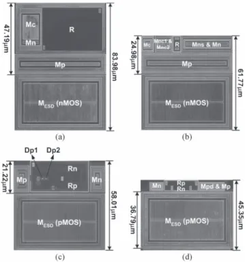
The test chips of power-rail ESD clamp circuits with the traditional RC-based, smaller capacitance, capacitor-less, and proposed high area-efficient ESD-transient detection circuits have been fabricated in a 65-nm 1.2-V CMOS process, as shown in Fig. 7(a)–(d). The dimension of MESDin all circuits verified in the silicon test chip is kept 2000 μm/100 nm. Compared with the traditional RC-based power-rail ESD clamp circuit, the layout area of the proposed power-rail ESD clamp circuit is reduced by∼46%, and the layout area of the high area-efficient ESD-transient detection circuit is reduced by ∼82%. These circuits are prepared for leakage measure-ment, ESD robustness and transmission line pulsing (TLP)
Fig. 7. Chip microphotograph of the fabricated power-rail ESD clamp circuits with the (a) traditional RC-based, (b) smaller capacitance, (c) capacitor-less, and (d) new proposed high area-efficient ESD-transient detection circuits.
Fig. 8. Measured leakage currents of fabricated power-rail ESD clamp circuits.
measurement, very fast TLP (VF-TLP) measurement, and turn-on verificatiturn-on.
A. Standby Leakage Current Measurement
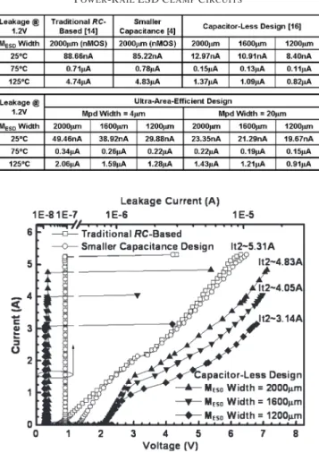
The leakage currents of the power-rail ESD clamp circuits are measured by HP4155 at 25 ◦C, as shown in Fig. 8. The leakage currents of the traditional RC-based and the smaller capacitance designs are 88.66 and 85.22 nA, respectively. At the same MESDwidth of 2000 μm, the leakage current of the capacitor-less design can be reduced to only 12.97 nA due to the ESD clamp pMOS transistor. For the proposed design, the leakage current is 23.35 nA for an Mpd width of 20 μm. Because the body node of MESDis not fully biased to VDD, the Mp would not be fully turned off to increase the leakage current [as shown in Fig. 5(a)]. Although the leakage current of the proposed design is slightly larger than that of the capacitor-less
Fig. 9. TLP measured I–V curves of the power-rail ESD clamp circuits with the traditional RC-based, smaller capacitance, and the capacitor-less designs.
design, it is still reduced by∼74%, compared with that of tra-ditional RC-based design. The leakage currents of the power-rail ESD clamp circuits at different temperatures are also listed in Table III. At higher temperatures, it can be observed that the increasing percentage of leakage current of the proposed design is much better than those of the prior art designs.
B. TLP Measurement and ESD Robustness
The TLP generator with a pulsewidth of 100 ns and a rise time of∼2 ns is used to measure the fabricated power-rail ESD clamp circuits [18]. The measured TLP I–V curves of the prior arts are shown in Fig. 9. The It2 values of the traditional RC-based and the smaller capacitance designs with an MESDwidth of 2000 μm are both 5.31 A. However, the It2 of the capacitor-less design is 4.83 A due to the ESD clamp pMOS transistor.
As shown in Fig. 10(a), the It2 of the proposed power-rail ESD clamp circuit can achieve the same level as that of capacitor-less design at the specific MESDwidth. To observe the beginning of conduction in Fig. 10(a), the zoom-in illustra-tion of TLP I–V curves is shown in Fig. 10(b). The curves of different Mpd widths start to rise at different voltage levels due to the body effect of MESD. For the Mpd width of 4 μm, the body effect is worse, and the threshold voltage of MESDwould
Fig. 10. Measured I–V curves of the proposed power-rail ESD clamp circuits under (a) the TLP measurement, (b) the zoom-in illustration of TLP I–V curves for observing the holding voltages, and (c) the dc I–V measurement by curve tracer.
be smaller. As a result, the TLP I–V curves for the Mpd width of 4 μm rise at lower voltage level of∼1.3 V (it is ∼1.8 V for the Mpd width of 20 μm). In addition, the dc I–V curves of the proposed designs are measured (using TEK370 curve tracer) by applying a voltage sweep on the VDD power line to verify the dependence on the body effect of MESDand the holding voltage
TABLE IV
ESD ROBUSTNESS OFFABRICATEDPOWER-RAILESD CLAMPCIRCUITS
Fig. 11. VF-TLP measured I–V curves of the high area-efficient power-rail ESD clamp circuits with an Mpd width of 20 μm under positive VDD-to-VSS ESD stress.
of the proposed power-rail ESD clamp circuit. In Fig. 10(c), the circuit with the Mpd width of 4 μm surely has lower holding voltage of∼1.76 V due to more serious body effect, and it is high, i.e.,∼1.95 V, for the Mpd width of 20 μm when the width of MESD is kept at 2000 μm. Overall, the measured holding voltages are all higher than the normal circuit operating voltage VDD of 1.2 V no matter what kind of measurement is taken. Hence, the proposed design is free to latchup issue for safely applying in 1.2-V applications [19], [20].
The measured HBM and machine-model (MM) [21] ESD levels under positive and negative VDD-to-VSS ESD stresses are listed in Table IV. The measured HBM (MM) ESD level of the ESD clamp pMOS transistor with the width of 2000 μm is over±8 kV (+500 V and −700 V). Overall, the measured HBM and MM ESD levels of the proposed power-rail ESD clamp circuits are well proportional to the width of MESD.
Charged-device model (CDM) is also an important ESD testing standard for ICs. In order to investigate the turn-on behavior of the proposed designs under CDM-like fast-transient condition, the VF-TLP with a pulsewidth of 10 ns and a rise time of 200 ps is used to measure the proposed power-rail ESD clamp circuits. The measured VF-TLP I–V curves of the power-rail ESD clamp circuits with different MESDwidths are shown in Fig. 11, where the width of Mpd is kept at 20 μm.
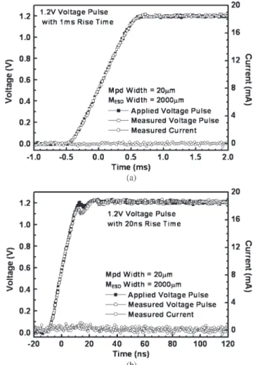
Fig. 12. Measured transient voltage and current waveforms of the high area-efficient power-rail ESD clamp circuit under the 1.2-V power-on transition with rise times of (a) 1 ms and (b) 20 ns.
In Fig. 11, the proposed power-rail ESD clamp circuits can be successfully activated to achieve higher It2 than those mea-sured by TLP measurement due to the shorter pulsewidth of VF-TLP. In addition, the measured It2 from VF-TLP is also well proportional to the width of MESD.
C. Turn-on Verification
For normal power-on condition, the voltage pulse usually has a rise time on the order of milliseconds. As shown in Fig. 12(a), the measured voltage on VDD power line successfully rises up to 1.2 V in 1 ms without any degradation, and the measured current is near zero. However, some previous studies [4], [11] have demonstrated that the power-rail ESD clamp circuits with RC-based ESD-transient detection circuits were easily mistriggered or into the latch-on state under the fast power-on condition. The proposed power-rail ESD clamp circuit has also been applied with 1.2-V voltage pulse with 20-ns rise time to investigate the immunity against mistrigger under the fast power-on condition, as shown in Fig. 12(b). The measured voltage on VDD power line still can rise up to 1.2 V with tiny deviation in the beginning period of∼5 ns. However, the measured current waveform is smooth at the level near zero. Therefore, the proposed power-rail ESD clamp circuit can be still free from the mistrigger issues.
Fig. 13. Measured voltage and current waveforms of the proposed power-rail ESD clamp circuit under (a) transient noise and (b) TLP transition conditions.
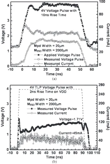
The transient voltage with a pulse height of 4 V and a rise time of 10 ns is applied to the VDD power line with 1.2-V normal operation voltage to verify the latch-on issue. As shown in Fig. 13(a), the transient voltage pulse can activate the ESD-transient detection circuit to command MESD at “ON” state. The applied 4-V voltage pulse is clamped down to a lower voltage level of ∼2.2 V by the proposed power-rail ESD clamp circuit with a discharging current of ∼35 mA. After the transient, the voltage on VDD power line is back to 1.2-V operation voltage, and the current is almost zero.
In order to observe the transient behavior of the proposed power-rail ESD clamp circuit, a TLP voltage pulse with a rise time of 2 ns and a pulse height of 4 V is applied to the VDD power line with the VSS grounded. The TLP voltage pulse can quickly initiate the proposed power-rail ESD clamp circuit. The measured voltage and current waveforms in time domain on VDD power line under 4-V voltage pulse are shown in Fig. 13(b). The applied 4-V voltage pulse can be quickly clamped down to a lower voltage level of ∼1.71 V by the proposed power-rail ESD clamp circuit with the discharging current of ∼45 mA. When the TLP voltage pulse height is increased, the proposed power-rail ESD clamp circuit can dis-charge more current. The turned-on MESDcan provide a low-impedance path from VDD to VSS to discharge ESD current and clamp down the voltage level. Overall, the proposed high
the parasitic diodes as equivalent capacitors to form the equiva-lent RC-based ESD-transient detection mechanism. According to the measured results, the proposed power-rail ESD clamp circuit has excellent immunity against the transient-induced latch-on or mistrigger issues and good proportionality between the width of MESDand the ESD robustness. Moreover, the high area-efficient ESD-transient detection circuit saves the layout area by ∼82% compared with the traditional RC-based one. The proposed power-rail ESD clamp circuit is an excellent circuit solution to achieve effective and efficient on-chip ESD protection in advanced nanoscale CMOS process.
ACKNOWLEDGMENT
The authors would like to thank T. Hasebe, K. Hasegawa, and M. Sawada for the help of VF-TLP measurement from Hanwa Electronic Ind. Co., Ltd., Japan.
REFERENCES
[1] M. Stockinger, J. Miller, M. Khazhinsky, C. Torres, J. Weldon, B. Preble, M. Bayer, M. Akers, and V. Kamat, “Boosted and distributed rail clamp networks for ESD protection in advanced CMOS technologies,” in Proc. EOS/ESD Symp., 2003, pp. 17–26.
[2] J. Li, R. Gauthier, and E. Rosenbaum, “A compact, timed-shutoff, MOSFET-based power clamp for on-chip ESD protection,” in Proc. EOS/ ESD Symp., 2004, pp. 273–279.
[3] J. Li, R. Gauthier, S. Mitra, C. Putnam, K. Chatty, R. Halbach, and C. Seguin, “Design and characterization of a multi-RC-triggered MOSFET-based power clamp for on-chip ESD protection,” in Proc. EOS/ESD Symp., 2006, pp. 179–185.
[4] S.-H. Chen and M.-D. Ker, “Area-efficient ESD-transient detection circuit with smaller capacitance for on-chip power-rail ESD protection in CMOS ICs,” IEEE Trans. Circuits Syst. II, Exp. Briefs, vol. 56, no. 5, pp. 359– 363, May 2009.
[5] J. C. Smith and G. Boselli, “A MOSFET power supply clamp with feedback enhanced triggering for ESD protection in advanced CMOS technologies,” in Proc. EOS/ESD Symp., 2003, pp. 8–16.
[6] J. C. Smith, R. A. Cline, and G. Boselli, “A low leakage low cost-PMOS based power supply clamp with active feedback for ESD protection in 65 nm CMOS technologies,” in Proc. EOS/ESD Symp., 2005, pp. 298–306. [7] M.-D. Ker and J.-H. Chen, “Self-substrate-triggered technique to enhance
turn-on uniformity of multi-finger ESD protection devices,” IEEE J. Solid-State Circuits, vol. 41, no. 11, pp. 2601–2609, Nov. 2006. [8] H. Wolf, H. Gieser, and W. Stadler, “Bipolar model extension for MOS
transistors considering gate coupling effects in the HBM ESD domain,” in Proc. EOS/ESD Symp., 1998, pp. 271–280.
[9] G. Notermans, A. Heringa, M. Van Dort, S. Jansen, and F. Kuper, “The effect of silicide on ESD performance,” in Proc. IEEE Int. Rel. Phys. Symp., 1999, pp. 154–158.
[10] K.-H. Oh, C. Duvvury, K. Banerjee, and R. W. Dutton, “Investigation of gate to contact spacing effect on ESD robustness of salicided deep submicron single finger NMOS transistors,” in Proc. Int. Rel. Phys. Symp., 2002, pp. 148–155.
[11] C.-C. Yen and M.-D. Ker, “The effect of IEC-like fast transients on RC-triggered ESD power clamps,” IEEE Trans. Electron Devices, vol. 56, no. 6, pp. 1204–1210, Jun. 2009.
[12] T. J. Maloney and W. Kan, “Stacked PMOS clamps for high voltage power supply protection,” in Proc. EOS/ESD Symp., 1999, pp. 70–77. [13] G. Boselli, C. Duvvury, and V. Reddy, “Efficient pnp characteristics of
pMOS transistors in sub-0.13 μm ESD protection circuits,” in Proc. EOS/ESD Symp., 2002, pp. 260–269.
[14] M.-D. Ker, “Whole-chip ESD protection design with efficient VDD-to-VSS ESD clamp circuits for submicron CMOS VLSI,” IEEE Trans. Elec-tron Devices, vol. 46, no. 1, pp. 173–183, Jan. 1999.
[15] “Electrostatic Discharge Sensitivity Testing—Human Body Model (HBM)—Component Level,” Rome, NY, USA, Test Method ESD STM5.1, 2001.
[16] C.-T. Yeh, Y.-C. Liang, and M.-D. Ker, “PMOS-based power-rail ESD clamp circuit with adjustable holding voltage controlled by ESD detection circuit,” in Proc. EOS/ESD Symp., 2011, pp. 1–6.
[17] M.-D. Ker and C.-C. Yen, “Investigation and design of on-chip power-rail ESD clamp circuits without suffering latchup-like failure during system-level ESD test,” IEEE J. Solid-State Circuits, vol. 43, no. 11, pp. 2533– 2545, Nov. 2008.
[18] T. J. Maloney and N. Khurana, “Transmission line pulsing techniques for circuit modeling of ESD phenomena,” in Proc. EOS/ESD Symp., 1985, pp. 49–54.
[19] M.-D. Ker and S.-F. Hsu, Transient-Induced Latchup in CMOS Integrated Circuits. New York, NY, USA: Wiley, 2009.
[20] M.-D. Ker and S.-F. Hsu, “Physical mechanism and device simulation on transient-induced latchup in CMOS ICs under system-level ESD test,” IEEE Trans. Electron Devices, vol. 52, no. 8, pp. 1821–1831, Aug. 2005. [21] “Electrostatic Discharge Sensitivity Testing—Machine Model (MM)—
Component Level,” Rome, NY, Test Method ESD STM5.2, 1999.
Chih-Ting Yeh (S’10) received the M.S. degree
from the Institute of Electronics, National Chiao-Tung University, Taiwan, in 2006, where he is cur-rently working toward the Ph.D. degree.
He is also with the Industrial Technology Research Institute, Taiwan.
Ming-Dou Ker (F’08) received the Ph.D. degree
from the Institute of Electronics, National Chiao-Tung University (NCTU), Taiwan, in 1993.
He is currently the Dean of the College of Photonics, NCTU, and also the Editor of IEEE TRANSACTIONS ON DEVICE AND MATERIALS
![Fig. 3. Capacitor-less power-rail ESD clamp circuit with diode string in the ESD-transient detection circuit and ESD clamp pMOS transistor [16].](https://thumb-ap.123doks.com/thumbv2/9libinfo/7635683.136371/2.891.84.380.105.532/capacitor-circuit-string-transient-detection-circuit-clamp-transistor.webp)