矽鍺薄膜在不同氧化條件下之電性研究
45
0
0
全文
(2) 矽鍺薄膜在不同氧化條件下之電性研究. A Study of Electrical Properties of SiGe Film with Various Oxidation Conditions. 研 究 生:吳資麟. Student:Tzu-Lin Wu. 指導教授:張國明 博士. Advisor:Dr. Kow-Ming Chang. 桂正楣 博士. Dr. Cheng-May Kwei. 國 立 交. 通 大 學. 電子工程學系 電子研究所碩士班 碩. 士. 論. 文. A Thesis Submitted to Institute of Electronics College of Electrical Engineering and Computer Science National Chiao Tung University In Partial Fulfillment of the Requirements for the Degree of Master In Electronics Engineering. September 2006, Hsinchu, Taiwan, Republic of China 中華民國九十五年九月.
(3) 矽鍺薄膜在不同氧化條件下之電性研究. 研究生:吳資麟. 指導教授:張國明 博士 桂正楣 博士 國立交通大學 電子工程學系 電子研究所碩士班. 摘. 要. 近年來,隨著元件尺寸縮小,增加載子遷移率已成為提升元件效能的趨勢之 一,而電子及電洞遷移率皆高的矽鍺合金在此情況下也自然而然地被廣泛研究。 藉由對矽鍺合金氧化,我們可以輕易提高鍺在矽鍺合金中的比例,進而造成更高 的電子及電洞遷移率。在本實驗中,我們對矽鍺薄膜做了多種不同條件的氧化製 程,並且製作成為傳統的金氧半場效電晶體(MOSFET),藉由電性的量測,我們 研究不同氧化條件對於矽鍺-金氧半場效電晶體的電特性影響。從實驗中我們發 現,氧化溫度越高、時間越長、氧氣流量越大的元件,表現出較佳的電流特性; 而在氧化速率的實驗中,氧化較慢的元件則有較低的漏電流。在文中,我們嘗試 找出造成這些現象的可能原因,並且探討出最佳的氧化條件。. i.
(4) A Study of Electrical Properties of SiGe Film with Various Oxidation Conditions Student:Tzu-Lin Wu. Advisor:Kow-Ming Chang Cheng-May. Kwei. Department of Electronics Engineering & Institute of Electronics National Chiao Tung University. ABSTRACT. As channel length of metal-oxide-semiconductor field-effect transistors (MOSFETs) is deeply scaled down, enhancing the carrier mobility in the channel is desired for improving the performance of complementary MOS (CMOS) circuit. SiGe is a promising channel material because of its high electron and hole mobility. Higher Ge content in SiGe film makes higher mobility of both electrons and holes, and the oxidation process of SiGe is an easy way to achieve higher Ge content. In this study, various oxidation conditions were performed of SiGe film, and a conventional p-MOSFET was fabricated on it. I-V characteristics were measured to investigate the influence on electrical properties of the various oxidation conditions. It is found that the devices of higher oxidation temperature, longer oxidation time, and higher oxygen flow show better electrical performance. It is also found that devices under lower oxidation rate has lower leakage current and then induce higher On/Off ratio. Discussions of the results were made and the optimum condition of oxidation was therefore suggested.. ii.
(5) 誌. 謝. 首先,我要感謝指導教授張國明老師及桂正楣老師,老師們認真 的教學精神和開明的教學態度,使我這兩年研究生涯獲益匪淺,並讓 我能在自由且輕鬆的環境下致力於研究,在此致上最深的謝意。 謝謝郭俊銘學長在碩士班兩年間給予我的建議及協助,使我的實 驗能順利完成。也感謝吳恆信同學,有了他的幫忙與砥礪,使得研究 過程不再單調乏味。也要謝謝 632 實驗室的其他眾多學長們,有了他 們的協助,使得研究能夠更加完整。 謝謝交大奈米中心、國家奈米實驗室提供各種機台設備,讓我可 以進行實驗。 最後,更感謝我的父母,吳家駿先生與江小鳳女士,感謝他們對 我從小到大的養育及栽培,在生活上給我無微不至的關心,並在我情 緒低落時帶給我溫暖及鼓勵,讓我得以全心完成學業。我相信他們會 以我為榮。. iii.
(6) Contents. Chinese Abstract………………………………………………………………………i English Abstract……………………………………………………………………...ii Acknowledgement…………………………………………………………………...iii Contents……………………………………………………………………………...iv Table Captions…………………………………………………………………….…vi Figure Captions……………………………………………………………………..vii. Chapter 1 Introduction…………………………………………………………….... 1 1.1 An Overview of the Applications of High Mobility SiGe Alloy………. …... 1 1.2 Ge Condensation Process in SiGe Film.…………………………………….. 1 1.3 Mechanism of SiGe Oxidation……………………………………………… 2 1.4 Motivation…………………………………………………………………… 3 1.5 Thesis Organization…………………………………………………………. 4 1.6 Reference……………………………………………………………………. 4 Chapter 2 Experiment…………..………………………………….……………….. 7 2.1 The Process Flow of SiGe-based p-MOSFET…..……………...…………… 7 2.2 Methods of Measurements and Analysis……………………………………. 9 2.2.1 Current-Voltage Characteristic Measurement…………………...…… 9 2.2.2 The Introduction of HP4156A……………………………….………10 Chapter 3 Results and Discussions………………………………………...………12 3.1 Influence of Oxidation Temperature on Electrical Properties………………12 3.2 Influence of Oxidation Time on Electrical Properties…………...………….13 3.3 Influence of Oxygen flow on Electrical Properties…..……………………..14 3.4 Influence of the Thickness of Pre-oxide on Electrical Properties.………….14 iv.
(7) 3.5 Influence of Oxidation Rate on Electrical Properties.……………...……….15 Chapter 4 Conclusion…………………...………………………………………….17 Chapter 5 Future Work…………………………………………………….………18. v.
(8) Table Captions. Table 2-1(A). Experiment of Different Oxidation Temperature. Table 2-2(B). Experiment of Different Oxidation Time. Table 2-1(C). Experiment of Different Oxygen Flow. Table 2-1(D). Experiment of Different Pre-oxide Thickness. Table 2-1(E). Experiment of Different Oxidation Rate.. Table 3-1. Normalized data of I-V characteristics with different oxidation temperature. Table 3-2. Normalized data of I-V characteristics with different oxidation time. Table 3-3. Normalized data of I-V characteristics with different oxygen flow. Table 3-4. Normalized data of I-V characteristics with different thickness of pre-oxide. Table 3-5. Normalized data of I-V characteristics with different oxidation rate.. vi.
(9) Figure Captions. Fig. 2-1. Cross sectional view of SiGe-based P-MOSFET after mask #1. Fig. 2-2. Top view of SiGe-based P-MOSFET after mask #1. Fig. 2-3. Cross sectional view of SiGe-based P-MOSFET after mask #2. Fig. 2-4. Top view of SiGe-based P-MOSFET after mask #2.. Fig. 3-1(a). Id-Vg characteristics of different oxidation temperature. Fig. 3-1(b). gm-Vg characteristics of different oxidation temperature. Fig. 3-1(c). Id-Vg characteristics of different oxidation temperature. Fig. 3-2(a). Id-Vg characteristics after different oxidation time. Fig. 3-2(b). gm-Vg characteristics after different oxidation time. Fig. 3-2(c). Id-Vd characteristics after different oxidation time. Fig. 3-3(a). Id-Vg characteristics with different oxygen flow. Fig. 3-3(b). gm-Vg characteristics with different oxygen flow. Fig. 3-3(c). Id-Vd characteristics with different oxygen flow. Fig. 3-4(a). Id-Vg characteristics with different thickness of pre-oxide. Fig. 3-4(b). gm-Vg characteristics with different thickness of pre-oxide. Fig. 3-4(c). Id-Vd characteristics with different thickness of pre-oxide. Fig. 3-5(a). Id-Vg characteristics of different oxidation rate. Fig. 3-5(b). gm-Vg characteristics of different oxidation rate. Fig. 3-5(c). Id-Vd characteristics of different oxidation rate.. vii.
(10) Chapter 1 Introduction. 1.1 An Overview of the Applications of High Mobility SiGe Alloy. There are considerable interests in enhanced p-type metal-oxide-semiconductor field effect transistors (MOSFETs) for complementary logic applications, because of the inferior performance of conventional p-type MOS devices owing to the lower hole mobility. As Ge has the highest hole mobility of all semiconductors (1900 cm2/Vs), it attracts much attention to Ge or SiGe based p-type MOSFETs. Compared with Si, the hole mobility of Ge is about 5 times higher [1-2]. Unfortunately, growing thermal oxide on Ge usually results in a high density of interface traps [3]. Additionally, defect-free Ge cannot be grown directly on Si substrate due to the 4.2% lattice mismatch between the two materials [4-5]. High Ge content SiGe channels have been grown on Si substrates, using a graded SiGe buffer layer. This technique successfully utilized to achieve higher mobility in p-type MOSFET [6].. 1.2 Ge Condensation Process in SiGe Film. Conventionally, relaxed Si1-xGex film with high Ge content has been obtained by growing compositionally graded Si1-xGex much thicker than the critical thickness in order to introduce dislocations to relax strain in Si1-xGex layer [7]. Although the density of dislocations in the relaxed SiGe layer by this approach has been greatly reduced over time, the control of dislocations is still challenging and requires optimization for dislocation suppression. In addition, the thick Si1-xGex films need for 1.
(11) strain relaxation through dislocations (on the order of a few microns, with a typical grading rate of 10% germanium increment per micron) poses a serious bottleneck for throughput [8]. An approach to achieve high Ge content in relaxed Si1-xGex layer has been reported that takes the advantage of the selective removal of Si atoms from SiGe film by Si1-xGex thermal oxidation [9]. When the supply of Si atoms diffused from the SiGe to the oxidation interface meets the consumption of Si atoms during oxidation, only Si atoms would be oxidized because Si oxidation is preferred to Ge oxidation [10], which leads to an increased Ge content in the Si1-xGex layer as the film is thinned down.. 1.3 Mechanism of SiGe Oxidation. The oxidation of SiGe films has been studied to a great extent [11-12]. This is mainly because of the potential technological applications of the SiGe [13], but also because it was demonstrated that small amounts of Ge in Si or SiGe layer greatly enhance the rate of oxidation [14]. In all cases reported so far, oxidation of SiGe alloys resulted in a pure SiO2 layer, and a pileup of Ge at the oxide/SiGe interface [15-16]. Because of the large difference between the heat of formation of SiO2 (-204 kcal/mol) and GeO2 (-119 kcal/mol) [17], Si is more reactive than Ge while oxidation. As a result, the surface oxide is nearly pure SiO2, and Ge piles up underneath [19]. Some other features of SiGe oxidation are as follows: (1) During oxidation, Ge is completely rejected from the oxide. (2) There is no loss of Ge after oxidation. (3) The oxidation rate of SiGe in dry oxygen is mostly the same as that of pure Si. For wet oxidation, the rate of SiGe in the linear regime is 2 to 3 times higher than the rate of pure Si; but it is almost the same in the parabolic regime [19]. 2.
(12) Taking Ge concentration into consideration, it is found that GeO2 might form above pure SiO2 of those SiGe films with higher Ge content [20]. Below 50 at.% Ge, oxidation remains similar to what has been described above. For alloys containing above 50 at.% Ge, a markedly different behavior is found: A two-layer oxide is formed, consisting of a mixed ( Si, Ge ) O2 layer near the surface, and a pure SiO2 layer underneath [19]. According to the theory of binary alloy oxidation [21], at Si concentration lower than that at which Si becomes selectively oxidized (demonstrated to be 50 at.%), both Si and Ge will be simultaneously oxidized at the initial oxidation stage. As the oxidation proceeds, Ge gradually becomes depleted in the alloy phase in a zone next to the oxide/SiGe interface due to its higher growth rate [22], and the oxygen concentration is gradually getting lower. Eventually, oxide thickness will reach a critical value, which is proportional to the Ge concentration in SiGe film, such that the oxygen and Ge concentration at the oxide/SiGe interface are too low for Ge to be oxidized. At this stage a steady-state condition has been reached at which selective oxidation of Si succeeds and Ge piles up at the oxide/SiGe interface again. So that it is shown that Ge at the oxide/SiGe is in elemental form, while Ge at the oxide surface is in an intermediate oxidized form [23].. 1.4 Motivation. SiGe oxidation is widely used in either SiGe/Si hetro-junction devices, poly-SiGe gated MOSs, or SiGe channel devices. However, the optimal oxidation condition is not known yet. In this study, we adopt different oxidation temperature, oxidation time, oxygen flow, and oxidation rate to investigate the influence on the electrical characteristics of SiGe-based p-MOSFETs. I-V characteristics were measured by HP4156A. The optimization of oxidation 3.
(13) condition was also described to improve the electrical performance of the devices.. 1.5 Thesis Organization. In chapter 1, a brief overview of SiGe and its oxidation mechanism were introduced. In chapter 2, the fabrication process flow of SiGe-based p-MOSFET and the experimental recipes will be described. In chapter 3, the electrical characteristics of the devices through different recipes will be shown, and discussions of the results of different recipes will be made. In chapter 4, a conclusion is addressed. Finally, in chapter 5, future works as well as suggestion for further research will be given.. 1.6 References. [1] S. Takagi, A. Toriumi, M. Iwase, and H. Tango, IEEE Trans. Electron Devices 41, 2357, 1994. [2] S. M. Sze, Physics of semiconductor Devices (wiley-Interscience, New York, 1981), p.29. [3] K. Ismail, J. O. Chu, and B. S. Meyerson, Appl. Phys. Lett. 64, 23, 1994. [4] G. Hock, E. Kohn, C. Rosenblad, H. con Kanel, H.-J. Herzog and U.Konig., AIP, vol 76, 26, 2000. [5] Y. J. Mii, Y. H. Xie, E. A. Fitzgerald, D. Monroe, F. A. Theil, B. E. Weir, and L. C. Feldman, Appl. Phys. Lett. 59, 1611, 1991. [6] R. Schaffler, D. Tobben, H. Herzog, G. Abstreiter, and B. Hollander, Semicond. Sci. 4.
(14) Technol. 7, 260, 1992. [7] E. A. Fitzgerald, Y. H. Xie, M. L. Green, D. Brasen, A. R. Kortan, and J. Michel, Appl. Phys. Lett. 59, 811, 1991. [8] E. A. Fitzgerald, Y. H. Xie, D. Monroe, P. J. Silverman, J. M. Kuo, A. R. Kortan, F. A. Thiel, and B. E. Weir. Vac. Sci. Techol. B 10, 1807, 1992. [9] T. Tezuka, N. Sugiyama, T. Mizuno, and S. Takagi. Jpn. J. Appl. Phys. 40, 2866, 2001. [10] S.-G. Park, W. S. Liu, and M.-A. Nicolet, J. Appl. Phys. 75, 1764, 1994. [11] S. Margalit, A. Bar-lev, A. B. Kuper, H. Aharoni, and A. Neugroschel, J. Cryst. Growth 17, 288, 1972. [13] D. W. Goodman, Y. I. Nissin, E. Rosencher, Heterostructures on Silicon: One step Further with Silicon (Kluwer, Dordrecht, Boston, London, 1989). [14] O. W. Holland, C. White, and D. Fathy, Appl. Phys. Lett 51, 520, 1987. [15] D. Fathy, O. W. Holland, and C. White Appl, Phys. Lett 51, 1337, 1987. [16] G. L. Patton, S. S. Iyer, S. L. Delage, R. C. McIntosh, and E. Gannin, Mater. Res. Soc. Symp. Proc. 102, 295, 1988. [12] F. K. LeGoues, R. Rosenberg, and B. S. Meyerson, Appl, Phys, Lett. 54, 644, 1989. [17] CRC Handbook of Chemistry and Physics, 70th ed., edited by R. C. Weast, D. R. Lide, M. J. Astle, and W. H. Beyer (CRC, Boca Raton, 1989). [18] F. K. LeGoues, R. Rosenberg, T. Nguyen, F. Himpsel, and B. S. Meyerson, J. Appl. Phys. 65, 1724, 1989. [19] H. K. Liou, P. Mei, U. Gennser, and E. S. Yang, Appl, Phys, Lett. 59, 10, 1991. [20] J. Eugene, F. K. Legoues, V. P. Kesen, S. S. Iyer, and F. M. d’Heurle, Appl, Phys, Lett. 59, 1, 1991 [21] C. Wagner, J. Electronchem. Soc. 99, 369, 1952. 5.
(15) [22] C. Wagner, J. Electronchem. Soc. 103, 627, 1956. [23] J. Sladkova, Czech. J. Phys. B 27, 943, 197. 6.
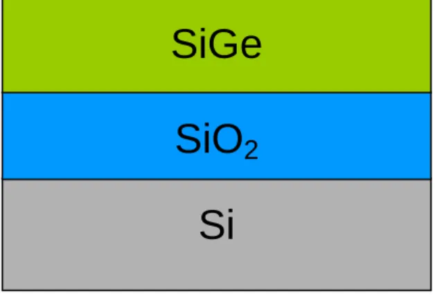
(16) Chapter 2 Experiment. 2.1 The Process Flow of SiGe-based P-MOSFET. P type (Boron doped) Si substrate (100) was used in this study. After initial RCA cleaning, 3000Å oxide was thermally grown at 980oC by horizontal furnace through wet oxidation, served as isolation layer. After one more time RCA cleaning, above is a 150Å thick amorphous-Si deposited by LPCVD at 550oC, as a buffer layer between SiO2 and SiGe film. SiGe (Ge content at 7% and 11%) film was then deposited onto amorphous-Si layer about 800Å by UHV-CVD. The cross sectional view is shown in figure 2-1. By means of photolithography, the active region could be defined after photo-resist has been removed. After S-D and channel patterning (top view shown in figure 2-2), TCP poly etcher was employed for SiGe etching by Cl2 and HBr. Later, the main part of this study proceeds by oxidizing the remaining SiGe part through different recipes. Different oxidation parameters like temperature, oxidation time, and oxygen flow were applied in order to find out the optimum oxidation condition of SiGe channel. Moreover, pre-deposited-oxide before oxidation, oxidation rate controlling were also performed trying to make better electrical characteristics performance of SiGe-based p-MOSFETs possible. All experimental factors are listed in table 2-1(A) to table 2-1(E). Next, devices were dipped in BOE solution to remove surface SiO2 formed during oxidation of SiGe film. After 1000Å SiO2 deposited by PECVD served as gate dielectic, 600oC anneal with O2 was performed to cure the defects in gate oxide for 30min. Then, 2000Å poly-Si was deposited by LPCVD to work as control gate. 7.
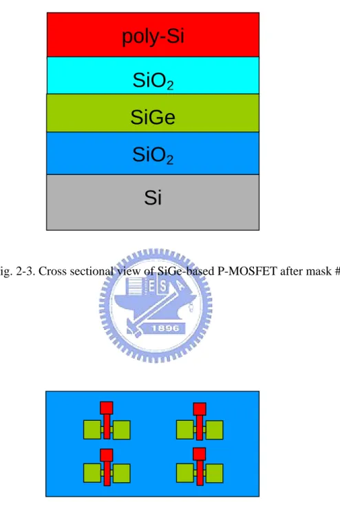
(17) After gate region and channel length defined by lithography, poly-etcher and BOE solution were used for etching. Cross sectional view and top view are shown in figure 2-3 and figure 2-4, respectively. Then, Boron was doped heavily with 5x1015 cm-2 at 10 keV. Activation annealing at 950oC in N2 flow was then employed for 30 minutes after ion implantation. 3000Å SiO2 by PECVD was deposited as passivation layer. Lithography comes next to form contact hole. SiO2 was then etched by BOE solution for about 55 seconds. Finally, a 500 nm Al film was deposited by evaporation and then contact pad were patterned. Al sintering was performed at 430oC for 30minutes. The detailed fabrication process flow is as follows: 1. (100) P+ Si wafer 2. RCA cleaning 3. Wet oxidation at 980oC for 3000Å 4. RCA cleaning 5. 150Å amorphous-Si by LPCVD 6. RCA cleaning 7. 800Å SiGe(Ge content at 7% and 11%) by UHVCVD 8. Mask #1:Define active region 9. Dry etching by TCP poly etcher 10. PR removing and RCA cleaning 11. SiGe dry oxidation 12. BOE dipped to remove SiO2 13. RCA cleaning 14. PECVD SiO2 1000Å deposition 15. Gate oxide annealing at 600o with O2 for 30min 16. LPCVD poly-Si 2000Å deposition 8.
(18) 17. Mask #2:Define gate region and channel length 18. Wet etching by poly-etcher solution for 90 seconds 19. Wet etching by BOE solution for 25 seconds 20. PR removing 21. Boron doping of 5x1015 cm-2 at 10 keV 22. Activation at 950oC for 30 minutes 23. STD cleaning 24. PECVD SiO2 3000Å deposition 25. Mask #3:Define contact hole 26. Wet etching by BOE solution for 50 seconds 27. PR removing 28. Al coating for 5000Å 29. Mask #4:Define contact pad 30. Al etching 31. PR removing 32. Sintering of Al at 430oC for 30 minutes. 2.2 Methods of Measurement and Analysis. 2.2.1 Current-Voltage Characteristic Measurement Current-Voltage characteristics were measured by a semiconductor parameter analyzer HP4156A at room temperature. Five devices of each sample were measured in order to choose a most reliable one to serve as result. Id-Vg characteristic was measured first. Then gm, on/off ratio and Vt could be calculated through Id-Vg characteristic data. Gm was defined as dId/dVg, and the maximum value of gm in each device was analyzed. Id-Vd characteristic was also 9.
(19) measure at a constant (Vg-Vt) value.. 2.2.2 The Introduction of HP4156A HP4156A is an electronic instrument for measuring and analyzing characteristics of semiconductor devices. This instrument is useful for performing both results measurements and analyses. Id-Vg and Id-Vd characteristics of our experiment were measure by HP4156A. There are four highly accurate source/monitor units (SMUs), two voltage source units (VSUs), and two voltage measurement units (VMUs) in HP4156A. HP4156A is designed for Kelvin connections and has high-resolution SMUs (HRSMUs), so HP4156A is especially suitable for low resistance and low current measurements. Voltage values with a resolution of 0.2μV can be measured by using the differential measurement mode of VMUs. Stress testing can be also performed by HP4156A. That is, a specified dc voltage or current can be forced on the device for a specified duration. Also, we can force ac stress by using pulse generator units (PGUs), which were installed in HP41501A SMU/Pulse Generator Expander. HP41501A is attached to HP4156A, and was equipped with a ground unit (GNDU), high power SMU (HPSMU), two medium power SMUs (MPSMUs), or two PGUs. HP4156A can print and store, in addition to perform measurement and analysis. Measurement setup information, measurement data, and instrument setting information can be stored in a 3.5-inch disk. The setting information and measurement results can be printed on a plotter or printer which is connected with HP4156A. HP4156A can be controlled by an external controller via HP-IB by using remote control commands. These commands are based on Standard Commands for 10.
(20) Programmable Instruments (SCPI), so measurement programs can be easily developed. HP4156A has internal HP instrument BASIC, so we can develop and execute measurement programs by using the HP4156A only, without using an external controller.. 11.
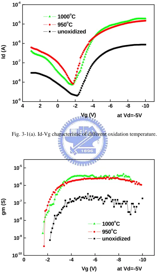
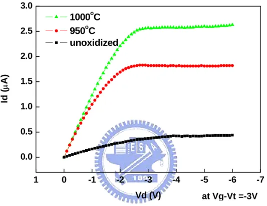
(21) Chapter 3 Results and Discussions. In the following chapter, all devices were normalized to W/L = 1μm/1μm. In Id-Vg and gm-Vg measurement, Vd was applied at -5V. While Id-Vd was measuring, |Vg-Vt| was set at 3V.. 3.1 Influence of Oxidation Temperature on Electrical Properties. Figure 3-1(a) shows Id-Vg characteristic of three different devices: un-oxidized, oxidation at 950oC, and oxidation at 1000oC. Si0.89Ge0.11 film was used in this experiment, and both of the oxidized devices were oxidized for 16 minutes with 3750 sccm O2 flow. It can be seen that both oxidized devices show superior electrical performance than the un-oxidized one by higher on/off ratio. The device of 1000oC-oxidized shows even higher on current than the one of 950oC-oxidized one while both devices have roughly the same off state current. Transconductance is shown in figure 3-1(b). Obviously, gm of 1000oC-oxidized device is higher than that of 950oC-oxidized one and of course than the un-oxidized one. They are about 3.78μS, 2.64μS, and 0.33μS, respectively. Figure 3-1(c) shows Id-Vd characteristic which is consistent with the prediction: the device oxidized at 1000oC has highest Id of the three devices -2.58μA at Vd=-6V. 950oC- oxidized device has 1.83μA , and the un-oxidized one has 0.40μA. It is known that since SiGe got oxidized, concentration of Ge would be increased, and then mobility would also get enhanced which resulted in a higher transconductance and on state current. As the improvement of on state current is 12.
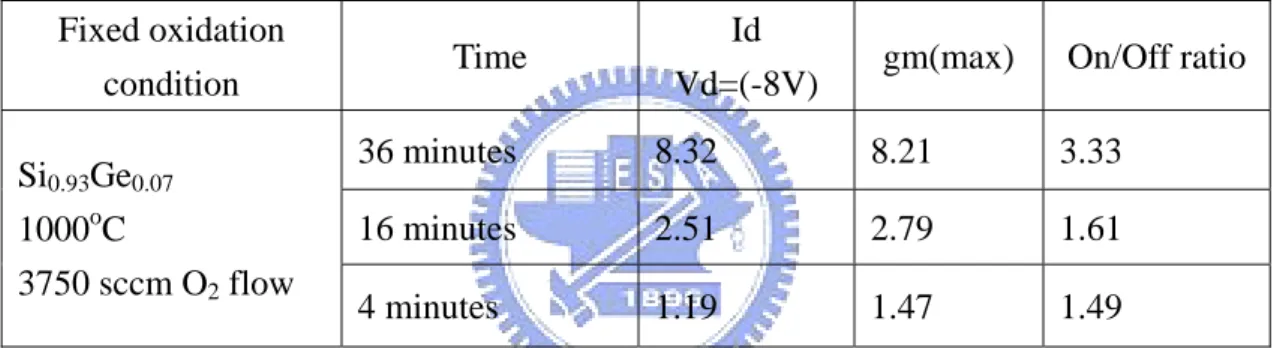
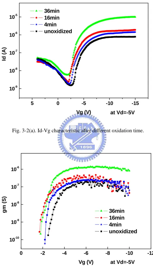
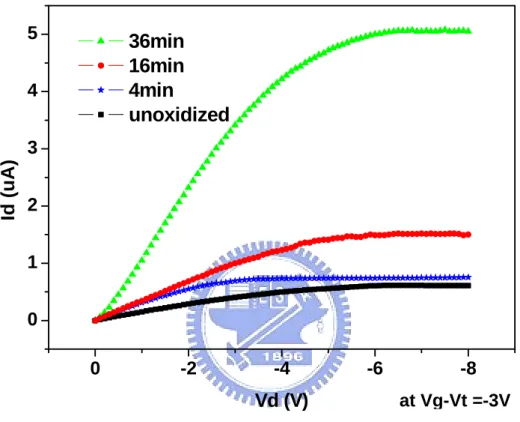
(22) higher than the increasing of off state current, on/off ratio gets improved then. With higher oxidation temperature, the rate of oxidation would be higher, which makes more Si in SiGe film oxidized. Then the mobility would be even higher, and better performance is achieved. Table 3-1 shows the normalized data which is divided by the results of un-oxidized device.. 3.2 Influence of Oxidation Time on Electrical Properties. Figure 3-2(a) shows Id-Vg characteristic of four different devices: un-oxidized, oxidized for 4 minutes, oxidized for 16 minutes, and oxidized for 36 minutes, respectively. Si0.93Ge0.07 film was used in this experiment. All of the oxidized devices were oxidized at 1000oC with 3750 sccm O2 flow. From the diagram, the trend of the curves indicates that longer oxidation time results in higher on state current and also higher transconductance (from Figure 3-2(b)). Besides, after calculation, the on/off ratio of 36min-oxidized, 16min-oxidized, and 4min-oxidized is 3.3, 1.6, 1.5 times higher than un-oxidized device, respectively. Due to the same reason as described in the previous section, in the longer oxidation time devices, more amount of Si was oxidized and then higher Ge concentration was achieved. So, similar trend of I-V characteristic as the previous section would be found in the diagram. Figure 3-3(c) depicts Id-Vd characteristic for devices with different oxidation time. As predicted, 36min-oxidized device has highest on current, which is 5.08μA at Vd=-8V. For the other devices, they are 1.52μA, 0.75μA, and 0.61μA for 16min-oxidized, 4min-oxidized, and un-oxidized device, respectively. Table 3-2 shows the normalized data which is divided by the results of un-oxidized device. It is presumed that unless Si in the SiGe layer is fully oxidized, the performance of the SiGe-based p-MOSFET would always be improved with the increasing of 13.
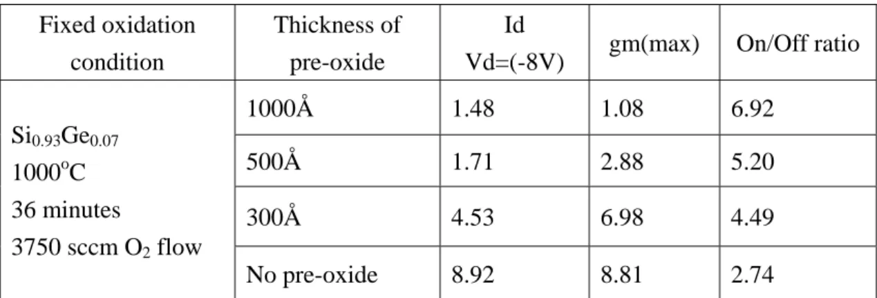
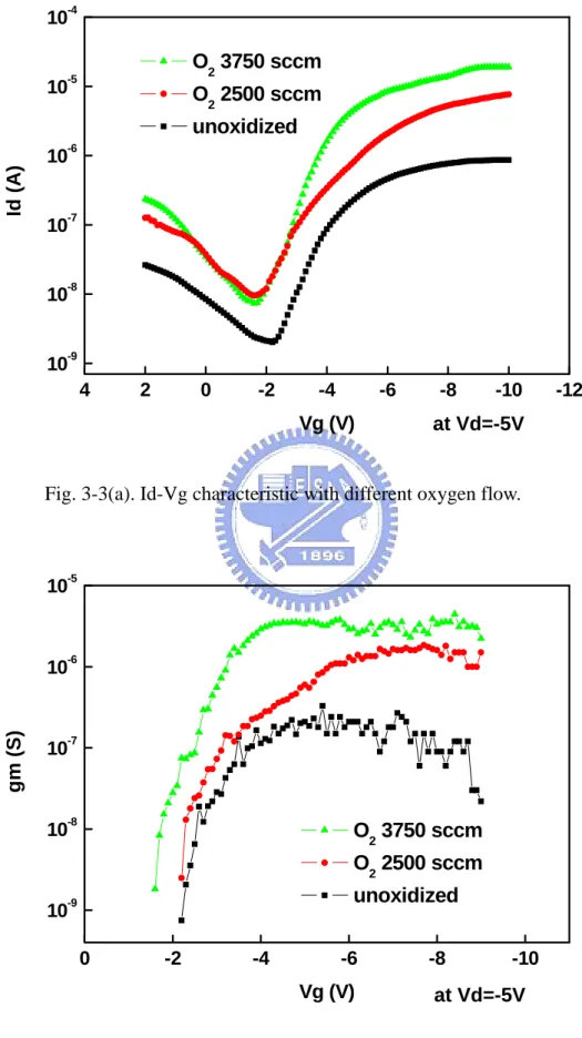
(23) oxidation time since the positive correlation between the amount of oxidized Si and the mobility of SiGe channel.. 3.3 Influence of Oxygen flow on Electrical Properties. Si0.89Ge0.11 film was used in this experiment. Devices were oxidized at 1000oC for 16minutes. Figure 3-3(a) depicts Id-Vg characteristic of devices with different oxygen flow during oxidation: 3750 sccm, 2500 sccm, and un-oxidized. The device under larger oxygen flow shows larger on state current, lower off state current, and higher transcondutance, which is undoubtedly better than the device oxidized under 2500 sccm oxygen flow and the un-oxidized one. It is supposed to be contributed by more Si being oxidized, as discussed already. The on/off ratio of 3750sccm-device and 2500sccm-device are 5.89 and 1.86 times higher than the un-oxidized one. Gm-Vg characteristic is shown in figure 3-2(b). As to Id-Vd characteristic, which is shown in figure 3-3(c), the device with 3750 sccm O2 flow has 2.56μA at Vd=-6V. The device with 2500 sccm O2 flow and un-oxidized has 1.83μA and 0.43μA, respetively. Table 3-3 shows the normalized data which is divided by the results of un-oxidized device. From 3-1 to 3-3, the amount of oxidized Si explans the improvement of electrical charateristic performance well. In the following three sections, several different oxidation condition were applied, and some other results would be achieved.. 3.4 Influence of the Thickness of Pre-oxide on Electrical Properties. As it is known that oxidation rate would decrease as oxidation proceeds with time, a new experiment is designed to investigate the influence of the initial oxidation 14.
(24) rate on electrical performance of SiGe-based p-MOSFET. SiO2 was deposited onto SiGe film first by PE-CVD right after UHV-CVD SiGe film was deposited. The thickness of SiO2 was 300Å, 500Å, and 1000Å, respectively, and a non-pre-oxide device was also fabricated. Si0.93Ge0.07 was used in this experiment and oxidation was performed at 1000oC for 36 minutes with 3750 sccm O2 flow. Figure 3-4(a) depicts Id-Vg characteristic of devices with different thickness of pre-oxide. The on/off ratio is getting higher while the thickness of pre-oxide getting larger, which is 2.6, 1.9, 1.7 times higher than non-pre-oxide device, respectively. But in the other hand, the on state current decreases. In figure 3-4(b), it is found that gm also gets lower with the increasing of pre-oxide thickness. It is presumed that less amount of Si in SiGe film would be oxidized owing to thicker pre-oxide exists, so that results in lower on current and transconductance. As shown in figure 3-4(c), Id at Vd=-8 of non-pre-oxide, 300 Å, 500 Å, and 1000 Å are 5.46μA, 2.79μA, 1.07μA, and 0.95μA, respectively. Table 3-4 shows the normalized data which is divided by the results of un-oxidized device. But there is still benefit from depositing pre-oxide. Since the oxidation rate was lowered by pre-oxide, a high quality channel was formed, which lowers the off state current, and results in a higher on/off ratio. The trade off between the on/off ratio and on state current should be considered case by case of the different use of the devices.. 3.5 Influence of Oxidation Rate on Electrical Properties. In the previous section, it is concluded that under lower oxidation rate, SiGe-based p-MOSFET would achieve better on/off ratio performance. But the amount of oxidized of Si in last experiment was still a variable. In this section, the factor of the amount of oxidized of Si was removed by a new designed method. 15.
(25) Several oxidation conditions were performed first and the thickness of SiO2 was measured. Three oxidation conditions of roughly the same thickness of SiO2 were selected. They are 950oC 15 minutes, 900oC 30 minutes, and 850oC 75 minutes, respectively, which indicates same amount of Si was oxidized. Si0.93Ge0.07 was used in this experiment and oxidation was performed with 3750 sccm O2 flow. Figure 3-5(a) depicts Id-Vg characteristic at Vd=-5V. On state current of the three devices almost equals, but the device with lower oxidation rate has lower off state current, which supports our conclusion from the previous section. As to gm-Vg characteristic in figure 3-5(b), three devices also have about the same gm, 0.5 ~ 0.6μ S. In figure 3-5(c), it is shown that the on state current of the three devices are also almost the same at about 2.1 ~ 2.3μA. Table 3-5 shows the normalized data which is divided by the results of un-oxidized device. As prediction, same amount of oxidized Si results in same gm and Id. Slow oxidation makes channel quality higher and then lower the off state current, resulting in a higher on/off ratio.. 16.
(26) Chapter 4 Conclusion. In this experiment, SiGe-based p-MOSFETs were fabricated and the electrical performance of the devices was improved by dry oxidation of SiGe channel through different recipes. First, it is found that all the electrical characteristics such as on/off ratio, on state current, and transconductance would get improvement after the SiGe channel was oxidized. This is because after oxidation, Si atoms in SiGe channel would be combined with O atoms to form SiO2 while Ge atoms would be separated from that. This is the so called Ge segregation mechanism. The more amount of Si in the SiGe film was oxidized, the more Ge atoms would exist in the SiGe channel and then makes Ge concentration higher which results in higher hole mobility in SiGe-base p-MOSFET. With the amount of oxidized Si increasing, the hole mobility also increases and then better electrical performance would be achieved. Experiments of oxidation temperature, oxidation time, and oxygen flow already proved this phenomenon. Oxidation rate was also considered in our experiment. The results show that the devices under slower oxidation rate have lower leakage current and better on/off ratio. It is conjectured that under slow oxidation process a high quality channel was formed. This is why the devices have lower leakage current.. 17.
(27) Chapter 5 Future Work. Since it is known that as the amount of oxidized Si increases, the electrical performance of SiGe-based p-MOSFET would get better, higher temperature like 1050oC, higher O2 flow such as 5000 sccm, and longer oxidation time could be applied in the same experiment to find the optimum situation of oxidation. Whether dry oxidation or wet oxidation differs is also a way of research. Same experiment can be also repeated in some other SiGe film with higher Ge content. Thermal oxide instead of PE-SiO2 serves as gate oxide may also bring expected improvement. As the best condition is found, fabrication of SiGe layer with high Ge concentration may be more economical and convenient through this Ge condensation method.. 18.
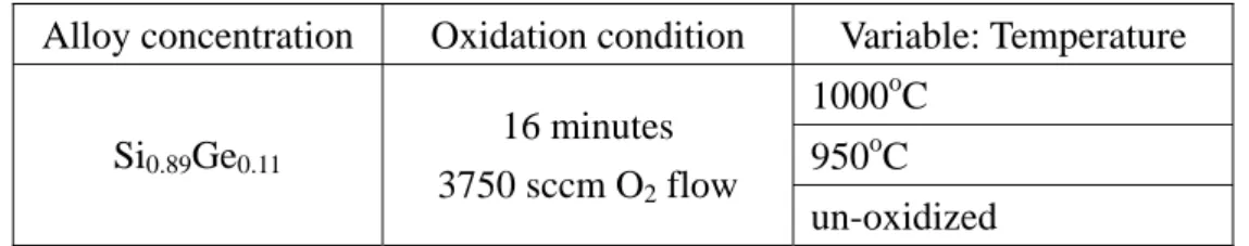
(28) Alloy concentration Si0.89Ge0.11. Oxidation condition 16 minutes 3750 sccm O2 flow. Variable: Temperature 1000oC 950oC un-oxidized. Table 2-1(A). Experiment of the Different Oxidation Temperature.. Alloy concentration. Oxidation condition. Variable: Time 36 minutes. o. Si0.93Ge0.07. 1000 C 3750 sccm O2 flow. 16 minutes 4 minutes un-oxidized. Table 2-1(B). Experiment of the Different Oxidation Time.. Alloy concentration. Oxidation condition. Si0.89Ge0.11. 1000oC 16 minutes. Variable: O2 Flow 3750 sccm 2500 sccm un-oxidized. Table 2-1(C). Experiment of the Different Oxygen Flow.. 19.
(29) Alloy concentration. Oxidation condition. Si0.93Ge0.07. 1000oC 36 minutes 3750 sccm O2 flow. Variable: Thickness 1000Å 500Å 300Å no pre-oxide. Table 2-1(D). Experiment of the Different Pre-oxide Thickness.. Alloy concentration. Oxidation condition. Variable: Rate o. 950 C 15 minutes Si0.93Ge0.07. 3750 sccm O2 flow. 900 oC 30 minutes 850 oC 75 minutes. Table 2-1(E). Experiment of the Different Oxidation Rate.. 20.
(30) Fixed oxidation condition Si0.89Ge0.11 16 minutes 3750 sccm O2 flow. Id Vd=(-6V). Temperature. gm(max). On/Off ratio. 1000 oC. 4.58. 8.02. 4.14. 950 oC. 6.45. 11.51. 6.02. Table 3-1. I-V characteristics with different oxidation temperature. Data was normalized by being divided by un-oxidized device.. Fixed oxidation condition Si0.93Ge0.07 1000oC 3750 sccm O2 flow. Id Vd=(-8V). Time. gm(max). On/Off ratio. 36 minutes. 8.32. 8.21. 3.33. 16 minutes. 2.51. 2.79. 1.61. 4 minutes. 1.19. 1.47. 1.49. Table 3-2. I-V characteristics with different oxidation time. Data was normalized by being divided by un-oxidized device.. Fixed oxidation condition Si0.89Ge0.11 16 minutes 1000oC. Id Vd=(-6V). O2 flow. gm(max). On/Off ratio. 3750 sccm. 6.02. 11.28. 5.89. 2500 sccm. 4.31. 5.64. 1.86. Table 3-3. I-V characteristics with different oxygen flow. Data was normalized by being divided by un-oxidized device.. 21.
(31) Fixed oxidation condition Si0.93Ge0.07 1000oC 36 minutes 3750 sccm O2 flow. Thickness of pre-oxide. Id Vd=(-8V). gm(max). On/Off ratio. 1000Å. 1.48. 1.08. 6.92. 500Å. 1.71. 2.88. 5.20. 300Å. 4.53. 6.98. 4.49. No pre-oxide. 8.92. 8.81. 2.74. Table 3-4. I-V characteristics with different thickness of pre-oxide. Data was normalized by being divided by un-oxidized device.. Fixed oxidation condition. Si0.93Ge0.07 3750 sccm O2 flow. Oxidation Rate. Pre-oxide Id gm(max) thickness Vd=(-6V). On/Off ratio. 950oC 15 minutes. 257Å. 3.92. 3.43. 4.11. 900oC 30 minutes. 261Å. 3.69. 3.30. 6.51. 850oC 75minutes. 266Å. 3.51. 3.61. 13.47. Table 3-5. I-V characteristics with different oxidation rate. Data was normalized by being divided by un-oxidized device.. 22.
(32) SiGe SiO2 Si Fig. 2-1. Cross sectional view of SiGe-based P-MOSFET after mask #1.. Fig. 2-2. Top view of SiGe-based P-MOSFET after mask #1.. 23.
(33) poly-Si SiO2 SiGe SiO2 Si. Fig. 2-3. Cross sectional view of SiGe-based P-MOSFET after mask #2.. Fig. 2-4. Top view of SiGe-based P-MOSFET after mask #2.. 24.
(34) -4. 10. o. 1000 C o 950 C unoxidized. -5. 10. Id (A). -6. 10. -7. 10. -8. 10. -9. 10. 4. 2. 0. -2. -4. -6. -8. Vg (V). -10. at Vd=-5V. Fig. 3-1(a). Id-Vg characteristic of different oxidation temperature.. -5. 10. -6. gm (S). 10. -7. 10. -8. 10. o. 1000 C o 950 C unoxidized. -9. 10. -10. 10. 0. -2. -4. -6. Vg (V). -8. -10. at Vd=-5V. Fig. 3-1(b). gm-Vg characteristic of different oxidation temperature. 25.
(35) 3.0 o. 1000 C o 950 C unoxidized. 2.5. Id (µA). 2.0 1.5 1.0 0.5 0.0 1. 0. -1. -2. -3. Vd (V). -4. -5. -6. -7. at Vg-Vt =-3V. Fig. 3-1(c). Id-Vg characteristic of different oxidation temperature.. 26.
(36) 36min 16min 4min unoxidized. -5. 10. -6. Id (A). 10. -7. 10. -8. 10. -9. 10. 5. 0. -5. -10. Vg (V). -15. at Vd=-5V. Fig. 3-2(a). Id-Vg characteristic after different oxidation time.. -6. 10. -7. gm (S). 10. -8. 10. 36min 16min 4min unoxidized. -9. 10. -10. 10. 0. -2. -4. -6. Vg (V). -8. -10. at Vd=-5V. Fig. 3-2(b). gm-Vg characteristic after different oxidation time. 27. -12.
(37) 5. 36min 16min 4min unoxidized. 4. Id (uA). 3 2 1 0 0. -2. -4. Vd (V). -6. -8 at Vg-Vt =-3V. Fig. 3-2(c). Id-Vd characteristic after different oxidation time.. 28.
(38) -4. 10. O2 3750 sccm. -5. 10. O2 2500 sccm unoxidized. Id (A). -6. 10. -7. 10. -8. 10. -9. 10. 4. 2. 0. -2. -4. -6. Vg (V). -8. -10. at Vd=-5V. Fig. 3-3(a). Id-Vg characteristic with different oxygen flow.. -5. 10. -6. gm (S). 10. -7. 10. -8. 10. O2 3750 sccm O2 2500 sccm unoxidized. -9. 10. 0. -2. -4. -6. Vg (V). -8. -10. at Vd=-5V. Fig. 3-3(b). gm-Vg characteristic with different oxygen flow. 29. -12.
(39) 3.0. O2 3750 sccm. 2.5. O2 2500 sccm unoxidized. Id (µA). 2.0 1.5 1.0 0.5 0.0 0. -1. -2. -3. Vd (V). -4. -5. at Vg-Vt =-3V. Fig. 3-3(c). Id-Vd characteristic with different oxygen flow.. 30. -6.
(40) -5. 10. NO Pre-oxide 300A 500A 1000A. -6. Id (A). 10. -7. 10. -8. 10. -9. 10. -10. 10. 6. 4. 2. 0. -2. -4. -6. -8. Vg (V). -10. -12. at Vd=-5V. Fig. 3-4(a). Id-Vg characteristic with different thickness of pre-oxide.. -6. 10. gm (S). -7. 10. -8. 10. NO Pre-oxide 300A 500A 1000A. -9. 10. -10. 10. 2. 0. -2. -4. -6. Vg (V). -8. -10. -12. at Vd=-5V. Fig. 3-4(b). gm-Vg characteristic with different thickness of pre-oxide. 31.
(41) 6. NO Pre-oxide 300A 500A 1000A. 5. Id (µA). 4 3 2 1 0 0. -2. -4. Vd (V). -6. -8. at Vg-Vt =-3V. Fig. 3-4(c). Id-Vd characteristic with different thickness of pre-oxide.. 32.
(42) -5. 10. o. 950 C 15min o 900 C 30min o 850 C 75min. -6. Id (A). 10. -7. 10. -8. 10. -9. 10. 4. 2. 0. -2. -4. -6. Vg (V). -8. -10. at Vd=-5V. Fig. 3-5(a). Id-Vg characteristic of different oxidation rate.. -6. 10. -7. gm (S). 10. -8. 10. o. 950 C 15min o 900 C 30min o 850 C 75min. -9. 10. -10. 10. 0. -2. -4. -6. Vg (V). -8. -10. at Vd=-5V. Fig. 3-5(b). gm-Vg characteristic of different oxidation rate. 33. -12.
(43) 3. Id (µA). 2. 1 o. 950 C 15min o 900 C 30min o 850 C 75min. 0. 1. 0. -1. -2. -3. Vd (V). -4. -5. -6. at Vg-Vt =-3V. Fig. 3-5(c). Id-Vd characteristic of different oxidation rate.. 34. -7.
(44) 簡歷. 姓. 名:吳資麟. 性. 別:男. 出生日期:民國 69 年 12 月 22 日 出 生 地:台灣省台北市 住. 址:台中市陜西東五街 47 巷 9-3 號 4 樓. 學. 歷:國立台中一中. (民國 85 年 9 月~民國 88 年 6 月). 國立交通大學電子工程系. (民國 88 年 9 月~民國 93 年 6 月). 國立交通大學電子工程所. (民國 93 年 9 月~民國 95 年 9 月). 碩士論文:矽鍺薄膜在不同氧化條件下之電性研究 A Study of Electrical Properties of SiGe Film with Various Oxidation Conditions. 35.
(45) 簡歷. 姓. 名:吳資麟. 性. 別:男. 出生日期:民國 69 年 12 月 22 日 出 生 地:台灣省台北市 住. 址:台中市陜西東五街 47 巷 9-3 號 4 樓. 學. 歷:國立台中一中. (民國 85 年 9 月~民國 88 年 6 月). 國立交通大學電子工程系. (民國 88 年 9 月~民國 93 年 6 月). 國立交通大學電子工程所. (民國 93 年 9 月~民國 95 年 9 月). 碩士論文:矽鍺薄膜在不同氧化條件下之電性研究 A Study of Electrical Properties of SiGe Film with Various Oxidation Conditions.
(46)
數據
+7
相關文件
Isakov [Isa15] showed that the stability of this inverse problem increases as the frequency increases in the sense that the stability estimate changes from a logarithmic type to
Particularly, combining the numerical results of the two papers, we may obtain such a conclusion that the merit function method based on ϕ p has a better a global convergence and
It is well known that second-order cone programming can be regarded as a special case of positive semidefinite programming by using the arrow matrix.. This paper further studies
● Using canonical formalism, we showed how to construct free energy (or partition function) in higher spin theory and verified the black holes and conical surpluses are S-dual.
To improve the convergence of difference methods, one way is selected difference-equations in such that their local truncation errors are O(h p ) for as large a value of p as
As is known, practices of Medicine Buddha correspond to the concept of development of the pure land in the human world; since Master Taixu, Master Hong Yi and Master Yin Shun in
– One of the strengths of CKC Chinese Input System is that it caters for the input of phrases to increase input speed.. The system has predefined common Chinese phrases, such
• One of the strengths of CKC Chinese Input System is that it caters for the input of phrases to increase input speed. The system has predefined common Chinese phrases, such
