國立交通大學
顯示科技研究所
碩 士 論 文
紫外光保護層於有機薄膜電晶體之研究
Ultraviolet Light Protective Layer for
OTFTs Encapsulation
研
究 生:方俊傑
指導教授:冉曉雯
博士
紫外光保護層於有機薄膜電晶體之研究
研究生:方俊傑 指導教授:冉曉雯 博士
國立交通大學
顯示科技研究所碩士班
摘要
在這份論文中, 我們製造 N, N' bis(naphthalen 1 y) N, N'-bis(phenyl) 二氨基 聯苯(NPB)保護層保護有機薄膜電晶體(OTFTs)在紫外光照射之下免受退化。有 熱蒸鍍沉積的二氨基聯苯(NPB)薄膜之有機薄膜電晶體(OTFTs), 它被發現在紫 外光照射下所導致的退化能顯著減少。例如, 在大約紫外光照射 120 分鐘之後, 載子移動率的改變僅只 37 % 並且臨限電壓值的變動是在 10% 之內。相對地 , 沒有二氨基聯苯(NPB)薄膜的有機薄膜電晶體(OTFTs)遭受了嚴重的退化;載子 移動率大約減少 90%, 而臨限電壓值卻增加超過了 40%。有機薄膜電晶體 (OTFTs)因紫外光所導致的退化在此也被討論; 藉由原子力顯微鏡(AFM)的表面 形態分析和電子顯微鏡的化學分析(ESCA)得知, 五環素(pentacene)薄膜表面的 氧化和破壞是影響有機薄膜電晶體(OTFT)特性退化的主要因素。我們認為, 我 們的二氨基聯苯(NPB) 保護層是一個有用的方法保護五環素有機薄膜電晶體 (pentacene TFTs) 。Ultraviolet Light Protective Layer for OTFTs
Encapsulation
Student: Chun Chieh Fang Advisor:Dr. Hsiao-Wen Zan
Display Institude
National Chiao Tung University
Abstract
In this thesis, we fabricated N,N′-bis(naphthalen-1-y)-N,N′-bis(phenyl) benzidine (NPB) passivation to protect the organic thin-film transistors (OTFTs) from degradation under UV-light illumination. With a thermally-deposited NPB film on the OTFTs, it was found that UV-light induced degradation could be significantly reduced. For example, after about 120 minutes UV-light the change of field effect mobility was only 37 % and the change of threshold voltage was within 10%. On the contrary, the OTFTs without NPB film suffered serious degradation. The field-effect mobility was reduced by about 90%, and the threshold voltage was increased by more than 40%.
UV-light induced degradation on OTFTs was also discussed; Through surface morphology analysis by atomic force microscopy ( AFM ) and electron Spectroscopy for Chemical Analysis ( ESCA ) , the surface oxidation and destroyed pentacene
grains pentacene film was the dominative factor that influenced OTFT’s properties. We conclude that our NPB passivation is a promising way to protect pentacene TFTs.
Finally, I would like to address that the work is conducted under the leading of my supervisor and also Mr. Kuo-His Yen, Ph. D student in our lab. The result is shared with all the co-workers in this research.
誌謝
兩年時間的飛逝,回首兩年前,滿懷著夢想與期望來到交大。在交大的求 學過程中,遇到了許多困難與考驗,這些考驗使自己在思想或能力上都成長許 多。首先要感謝我的指導教授冉曉雯老師,感謝冉老師帶領我進入 OTFT 的世 界,以及在研究路上不厭其煩的指導我,使我有機會在這塊領域著墨,並從研 究當中讓我了解到一個研究者該有的執著與專業。 感謝實驗室的博班學長:國錫學長、政偉學長、士欽學長、蔚宗學長、文 元學長,在這兩年來的幫助與鼓勵。尤其是國錫學長,在我這兩年來的研究生 涯裡,用心的教導我實驗方法以及提供實驗上的想法,並在心情低落時給予我 適時的開導,且不辭辛勞地協助我完成我的碩士論文。感謝實驗室的同學:武 衛、權陵、旻君、和璁以及志宇,這兩年來的互相打氣,互相砥礪。感謝實驗 室的學弟妹們:繁琦、鈞銘、祥瑞、淑玲、玉玫…等,在苦悶的研究生活裡, 添加了許多歡樂,有你們的陪伴,讓我在這兩年的研究生涯中更為甘甜回味。 最後感謝我的爺爺、奶奶、父母、老哥以及妹妹,感謝你們一路的陪伴與 支持,沒有你們,就不會有今日的我。Contents
Abstract (Chinese)
Ι
Abstract (English)
ΙΙ
Acknowledgement
ΙV
Contents
V
Figure Captions
VΙΙΙ
Table Captions
XI
Chapter 1. Introduction
1-1 Introduction of Organic Thin Film Transistors (OTFTs) 1
1-2 Motivation 3
1-3 Thesis Organization 4
Chapter 2. Theoretical Background of OTFTs
2-1 Introduction 7
2-2 Transportation Mechanisms of Organic Semiconductor 7
2-3 Pentacene OTFTs with passivation layers 10
2-3-1 Environmental stability of pentacene thin-film transistors 2-3-2 High energy UV-light illumination on pentacene thin-film
2-4 Parameter Extraction 14 2-4-1 Mobility
2-4-2 Threshold voltage 2-4-3 Subthreshod swing 2-4-4 On/off ratio
2-4-5Gated four-probes for resistance
Chapter 3. Experiments
3-1 OTFTs Fabrication 23
3-2 UV illumination experiments. 25
Chapter 4. Result and Discussion
4-1 Degradation of pentacene OTFTs under UV-light illumination 28 4-1-1Electrical properties of un-passivated OTFTs under UV-light
illumination
4-1-2 Electrical properties of Gated-Four-Probes on un-passivated OTFTs under UV-light illumination
4-1-3 Material analysis on pentacene films
4-2 Ultraviolet light Protective Layer for OTFTspassivation 35 4-2-1 Transmittance and absorbing property of NPB passivation.
4-2-2 Electrical properties of NPB-passivated OTFTs under UV-light illumination
4-2-3Electrical properties of Gated-Four-Probes on NPB-passivated OTFTs under UV-light illumination
4-3 Comparison of un-passivated OTFTs and NPB-passivated OTFTs under UV-light illumination
40 4-3-1 Electrical properties of un-passivated OTFTs and NPB-passivated
OTFTs under UV-light illumination
4-3-2 Electrical properties of Gated-Four-Probes un-passivated OTFTs and Gated-Four-Probes passivated OTFTs under UV illumination
Chapter 5. Conclusion
. 5-1 Conclusion 58References
60Profile
68.
Figure Captions
Chapter 1
Fig. 1-1 Energy curve spectra of solar radiation at sea level Fig. 1-2 Energy curve spectra of the low-pressure tube Fig. 1-3 Absorption spectra of pentacene films
Chapter 2
Fig. 2-1 The X-ray diffraction (XRD) curves of pentacene film under different UV-light illumination times.
Fig. 2-2 UV-degeneration of electrical properties on pentacene TFTs Fig. 2-3 The Fourier transform infrared spectroscopy (FTIR) spectrum of
pentacene film under different UV-light illumination times Fig. 2-4 The structures of our flexible pentacene TFT with the SnO2
encapsulation layer prepared by IBAD: (a) schematic cross section (b) photographic plan view
Chapter 3
Fig. 3-1 The device structure of pentacene OTFTs with NPB passivation layer Fig. 3-2 The optical image of pentacene OTFTs with NPB passivation layer Fig.3-3 The image of UV illumination experiments
Chapter 4
Fig. 4-1 The transfer characteristics of pentacene OTFTs under different UV-light illumination times: Without passivation layer
threshold-voltage (VG−Vth ) of un-passivated OTFTs under UV-light
illumination , respectively.
Fig. 4-3 The △Rcont and △Rfilm and the percentage (%) of Rcont and Rfilm are
further plotted as a function of UV-light illumination times at VG−Vth=
-25 V .
Fig. 4-4 The X-ray diffraction (XRD) curves of pentacene film under different UV-light illumination times.
Fig. 4-5 The Raman spectrum of pentacene film under different UV-light illumination times
Fig. 4-6 The Fourier transform infrared spectroscopy (FTIR) spectrum of
pentacene film under different UV-light illumination times are shown in Fig. (a) and Fig. (b)
Fig. 4-7 The AFM images of pentacene films under different UV-light illumination times are shown in Fig. (a) ,. (b) , (c) , (d) ,(e) ,and (f).
Fig. 4-8 Electron Spectroscopy for Chemical Analysis (ESCA) under different UV-light illumination times : (a) Oxygen (O1s) and Carbon (C 1s) (b) Oxygen (O1s), and (c) Carbon (C 1s).
Fig. 4-9 Electron Spectroscopy for Chemical Analysis (ESCA) of depth profile under different UV-light illumination times
Fig. 4-10 The performance of the OTFT before and after the passivation with (a)TiO2 (b) NPB/Mg/TiO2 /PDMS (c)NPB
Fig. 4-11 The transmittance and absorption spectra of the film are obtained as presented in Figure (a) and Figure (b) , respectively
Fig. 4-12 The initial transfer characteristics with un-passivated OTFTs and passivated OTFTs , respectively.
Fig. 4-13 The transfer characteristics of pentacene OTFTs under different UV-light illumination times: Covered with NPB passivation layer.
Fig. 4-14 Figures. (a) and (b) presents the variation of the linear regime field-effect mobility and threshold voltage under UV-light illumination.
Fig. 4-15 The variation of the linear regime field-effect mobility under UV-light illumination.( the literatures with SnO2 film)
Fig. 4-16 The Rcont and the Rfilm is plotted as a function of gate-voltage minus
threshold-voltage ( VG−Vth =-25V) of un-passivated OTFTs and
NPB-passivated OTFTs under UV-light respectively. .
Table Captions
Chapter 2
Table 1 Summary list of current studies on OTFT passivation
Chapter 4
Table 2 The transfer characteristics of the OTFTs before and after passivation with TiO2 ,NPB, NPB/Mg/TiO2/PDMSlayers compared with literatures
Chapter 1
Introduction
1-1 Introduction of Organic Thin Film Transistors (OTFTs)
The concept of using organic materials as semiconductors layer in transistors are realized at least since the 1980s [1,2]. Recently , pentacene has received enormous attention as the most promising organic semiconductor for flexible displays, smart cards, radio frequency- identification tags , and various kinds of organic sensors[3-6]. Organic TFTs with mobility exceeding 1 cm2/v.s and an on/off ratio greater than 106
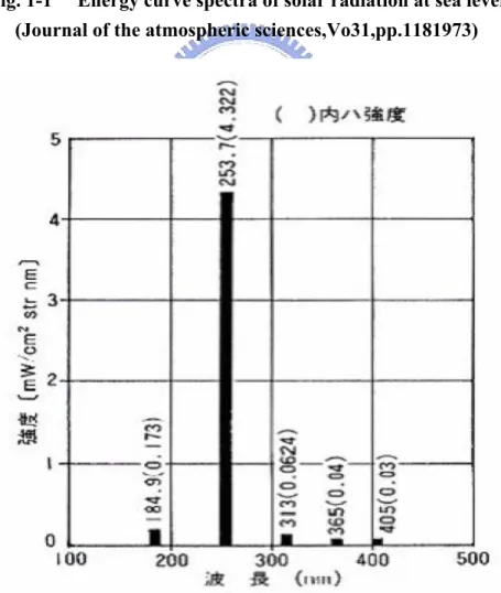
have been developed; these values are comparable to hydrogenated amorphous silicon transistors (a-Si:H TFT ) [7]. Nevertheless, there are still several issues to be considered before pentacene TFTs are launched into real applications: minimizing threshold voltage hysteresis, improving gate voltage stress resistance, and avoiding the environmental contamination or high-energy ultraviolet (UV)-induced degradation on the pentacene film.[8-10] Among these issues, the UV-induced degradation of pentacene is probably the most immediate and serious. Many studies reported the UV-degeneration effects on pentacene TFTs that were illuminated by a high energy UV with energy over 3.9 eV (wavelength shorter than ~320 nm). Though in a normal sea-level solar radiation the UV portion is very small(See Fig 1-1)[9-16].The
light-source such as fluorescent lamps and even the mercury light were the common source of UV-light. The low-pressure tube will emit short-wavelength radiation (185nm and 253.7nm from mercury vapor) which may cause damages to organic films(See Fig 1-2).However, in the present studies the details for UV degradation of device characteristics are still not well-understood.The performance of pentacene TFTs under high energy UV is also not reported.According to Jeong-M. Choi‘s research[11],when a high energy UV strikes the initial crystalline pentacene,it is likely that the pentacene channel gradually loses its crystallinity, enhancing the molecularlike character of constituent pentacenes inside as shown in Fig. 1-3.. In contrast, the energy of 364 nm UV is not high enough to generate crystalline defects in the pentacene channel. Light with energy larger than the energy gap of the respective semiconductor leads to a degradation of the devices.[15].Hence, it is important to discuss the device degradation under high energy UV illumination.
On the other hand , the stability of OTFTs is one of the major concerns. This is because, OTFTs or any other organic devices tend to easily degrade when they are directly exposed to ultraviolet (UV) lights with energy over 3.9 eV (wavelength shorter than ~320 nm)[13-15]. Although, Woo Jin Kim et.al[10] have reported on the fabrication of flexible pentacene thin-film transistors (TFTs) encapsulated with an ultraviolet (UV) protecting SnO2 thin film that has been prepared by
ion-beam-assisted deposition (IBAD). However, the SnO2 encapsulation involves ion beam processes that might cause a little damage on organic pentacene layer.In view of these facts, it is important to develop a protection technique for organic-based devices.
1-2 Motivation
In this experiment, we try to investigate that UV-light induced degradation on OTFTs.By the gated-4-probes OTFTs, the organic film properties and mental-contact effects can be studied separately. Moreover , it is conjected from material analysis to find what may be the dominative factor that influenced OTFT’s properties.
Finally ,we proposed on the fabrication of pentacene TFTs encapsulated with NPB thin-film that protect the organic thin-film transistors (OTFTs) from degradation under UV-light illumination.NPB film has high transparent property and does not damage on organic pentacene layer during the passivation process.
1-3 Thesis Organization
In Chapter 1, we make a brief introduction to the demands on OTFTs , passivation layer , and motivation of the thesis. In Chapter 2, we introduce the
transportation mechanisms of organic semiconductor, and parameter extraction. In Chapter 3, the fabrication and the structure of OTFTs are presented. In Chapter 4, the transmittance property of NPB passivation film , the transfer characteristics of un-passivated OTFTs and passivated OTFTs under UV-light illumination, and effects of UV light illumination on our OTFTs are investigated. Finally, we will make a conclusion in Chapter 5.
Fig. 1-1 Energy curve spectra of solar radiation at sea level (Journal of the atmospheric sciences,Vo31,pp.1181973)
Fig. 1-2 Energy curve spectra of the low-pressure tube
Fig. 1-2 Absorption spectra of pentacene films (Appl. Phys. Lett. , Vol. 90, pp.113515 2007 )
Chapter 2
Theoretical Background of OTFTs
2-1 Introduction
A large number of conjugated polymers, oligoacenes, and fused aromatics have been used to be the active layers of OTFTs. Most of these organic or polymer semiconductors are p-type material. Recently, many molecular semiconductors, such as pentacene, thiophene oligomers, and regioregular poly(3-alkyl-thiophene) are proposed. The most significant difference between distinguishing those devices fabrication is the deposition method. Among the p-type material , pentacene (C22H14)
is a rod-like aromatic molecule composed of five benzene rings, shows the highest mobility (>1cm2/v-sec), owning to highly ordered films with proper dielectric
properties and growth conditions. Hence, pentacene (C22H14) is a promising candidate
for future electronic devices and an interesting model system [17].
2-2 Transport Mechanisms of Organic Semiconductor
Carrier transport in the organic semiconductors have been investigated on the theory and modeling in the past years [18]. Organic conductors are conjugated materials, where the π-electrons are conducted intra the molecular. In conjugated
molecules , the properties of charge transport are intrinsically correlated with their crystalline structure, where the π delocalized carriers are responsible for the intra-molecular conduction.However, the nature of van der Waals bonding between discrete molecules is thought to be the limitation of the carrier transport, and the transport is usually described by “localized model “ Hence, the carrier transport is described by different models than the covalent-bonded semiconductors. In covalent-bonded semiconductors, carriers move as highly delocalized plane waves in wide bands and have a very high mobility. But in weak-bonded organic semiconductors, the high-mobility model is no longer valid.
Recently, two principal types of theoretical model are used to describe the transport in organic semiconductors : “The band-transport model” and “The hopping models”. However, band transport may not suit for some disordered organic semiconductors, in which carrier transport is govern by the hopping between localized states. Hopping is assisted by phonons and the mobility increases with temperature. Typically, the mobility is very low, usually much lower than 1cm2/V-sec. The
boundary between “band transport” and “hopping” is divided by materials mobilities (~1cm2/V-sec) at room-temperature (RT) [19]. Many kinds of polycrystalline
organic semiconductors , such as several members of the acene series including pentacene, rubrene, have RT mobility larger than 1cm2/V-sec. [20] Sometimes,
temperature-independent mobility was found in some polycrystalline pentacene devices [20]. Thus, this observation argued that the simply thermal activated hopping process governed the whole carrier transport behaviors in high quality polycrystalline pentacene film, despite that the temperature independent mobility has been observed in exceptional cases [21].
The understanding of carrier transport in single-crystal of organic semiconductors will help us to describe the transport mechanism in polycrystalline organic semiconductors. The coherent band-like transport of delocalized carriers becomes the prevalent transport-mechanism in the single crystals of organic semiconductors, such as pentacene, tetracene, under the low-temperature environments. A very high hole mobility values has been measured by time-of-flight experiments [22]. Thus, the temperature dependence of the carrier mobility was found below 100K and following with a power law of μ ∝ T-n, n~1, [23],
in single crystals of organic semiconductors, consistent with the band-transport model. However, between 100K and 300K, the carrier mobility show a constant value [23], that has been described as the superposition of two independent carrier transport mechanisms. The first mechanism was small molecular polaron (MP). According to this model, the carriers were treated as the heavy; polaron-type; quasi-particles. It is formed by the interaction of the carriers with intra-molecular vibrations of the local
lattice environment, and move coherently via tunneling. In this model, the mobility follows the power law μMP=aT-n. The other involves a small lattice polaron (LP),
which moves by thermally activated hopping and exhibits a typical exponential dependence of mobility on temperature : μLP=bexp[-Ea/kT]. The superposition of
these two mechanisms could get a good consistence with experimentally measurement of temperature-dependence mobility from room temperature to a Kelvin degrees (K) [24].
Finally, the exact nature of the charge carrier transport in organic molecular crystals is still not well-understood, which has been the focus in many theoretical studies [25].
2-3 Pentacene OTFTs with passivation layers
Organic thin-film transistors (OTFTs) have received increasing attention recently in place of conventional inorganic electronics because of advantages in their lower cost and simpler packaging, relative to conventional inorganic electronics, and their compatibility with flexible substrates[26-27]. For the commercial value of many applications based on organic devices, stability and performance of organic materials are important[27]. This is because that OTFTs or any other organic devices tend to easily degrade when they are directly exposed to ambient air with some degree of
humidity[28-30] or when exposed to UV-lights with energy over 3.9 eV (wavelength shorter than 320 nm)[13-15]. In view of these facts, it is important to develop a protection technique for organic-based devices.
2-3-1 Environmental stability of pentacene thin-film transistors
Recent studies on the environmental stability of OTFT indicate that some specific gases such as H2O and O2 affect the TFT performance significantly.[28-30]
For example, H2O remarkably degrades the performance of the OTFT without
encapsulation layers in ambient air. This is because that H2O can diffuse into the grain
boundaries and crystal lattice, and they capture charges generated in the channel because of its polar nature.[27,28,30] This results in the decrease in the on-current and field-effect mobility. On the other hand , in case of O2, because of its electronegativity,
it attracts the electrons from the pentacene molecules and generates holes.[31] Jurchescu et al. [31]suggested that oxygen accumulates holes within the pentacene layers by solving one-dimensional Fick’s second law. The dislocations in the pentacene crystal lead to accessible vacant orbital and enhance the chemical reactivity.[32] In other words, oxygen diffused to the grain boundaries does not contribute to form the accumulation of holes, but change pentacene into pentacenequinone by oxidation.[32] Therefore , in order to enhance the stability of devices, some encapsulation layers capable of preventing H2O or O2 in air from
penetrating through the organic layers have been employed.[33] SiOx, SiNx, AlOx, AlOxNy, SnO2 and SiOxNy are common amorphous oxides used as an inorganic gas
barrier[33-36]. Furthermore , parylene , polyvinylalcohol(PVA), photosensitive acryl ,and polydimethylsiloxanes(PDMS) are common organic materials used as an organic gas barrier[37-43].( The passivation layers summarized in Table1) .This is because these passivation layers which can perform the function of a gas barrier.[44] However, during the deposition process of the passivation layer, some serious damage might be induced on the organic layers. This damage would be caused by energetic ions, X-rays, or electron beams.[33,45-46]Therefore, finding a simple and suitable way to passivate or package organic devices has become an important subject.
2-3-2 High energy UV-light illumination on pentacene thin-film transistors
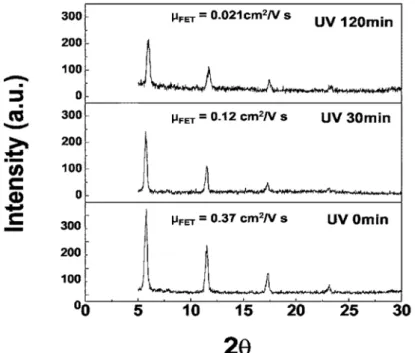
Many previous studies reported the UV-degeneration effects on pentacene TFTs when samples illuminated by a high-energy UV with energy over 3.9 eV (wavelength shorter than ~320 nm)[9-16]. In Woo Jin Kim ‘s research[10], according to X-ray diffraction data as shown in Fig.2-1 , they indicates that the UV-induced-degradation of device characteristics is directly correlated to the degradation of pentacene crystallinity against UV radiation. Furthermore, in Jeong-M. Choi‘s research[11] , according to the UV-degeneration of electrical properties on pentacene
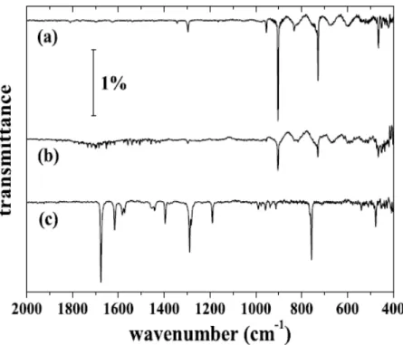
TFTs(SeeFig.2-2) , they signifies that the deep UV damaged the pentacene crystalline channel layer from the surface to the channel/gate oxide interface, generating excessive defects in the whole layer thickness. In particular, it is suspected that the deep UV may additionally cause a surface oxidation of organic pentacene, generating deep level defects near the surface in the vicinity of oxygen molecules in air. Finally in Woo Jin Kim ‘s research[12] , as shown in Fig.2-3 . absorption peaks characteristic of pentacene have decreased in intensity, and only a very weak and ill-defined broad feature between 1600 cm-1 and 1800 cm-1 (region of C–O stretching modes) appears
in the spectrum, which may indicate the formation of a variety of oxidized intermediate species (the tiny sharp absorptions in this region are due to residual water vapour in the spectrometer).Therefore, they indicates that the chemical reactions occurring in pentacene thin films in the presence of reactive oxygen species. As mentioned above, it is important to discuss the degradation of UV-light illumination on OTFTs.
On the other hand ,in order to protect the organic thin-film transistors (OTFTs) from degradation under UV-light illumination , Woo Jin Kim et.al[10] have reported on the fabrication of flexible pentacene thin-film transistors (TFTs) encapsulated with an ultraviolet (UV) protecting SnO2 thin film that has been prepared by
beam processes that might cause a little damage on organic pentacene layer. Therefore, before the IBAD processes , they were attempted on thermally evaporated buffer SnO2 on the top dense SnO2.(see.Fig2-4.) This makes the process complicated. In our research, a simple approach was demonstrated to protect organic devices from the damage of strong UV illumination.
2-4 Parameter Extraction
In this section, the methods of extraction the mobility, the threshold voltage, the subthreshold swing, the maximum interface trap density, and the is characterized, respectively.
2-4-1 Mobility
Generally, the linear mobility (for VD <VG−Vth) can be extracted from the
transconductance maximum g in the linear region: m
D OX t cons V G D m V L WC V I g D μ = ⎥ ⎦ ⎤ ⎢ ⎣ ⎡ ∂ ∂ = = tan (2.1)
The saturation mobility (for VD >VG−Vth) can also be extracted from the slope
of the curve in the squared drain-current versus the gate-voltage diagram: ( ) 2 OX G TH D C V V L W I = μ − (2.2)
2-4-2 Threshold voltage
Threshold voltage is related to the operation voltage and the power consumptions of an OTFT. We extract the threshold voltage from equation (2.2), the intersection point of the squared drain-current versus gate-voltage.
2-4-3 Subthreshold swing
Subthreshold swing is also important characteristics for device application. Its is a factor to estimate how rapidly the device switches from the off state to the on state in the region of exponential current increase. It is defined by:
∂
(
log)
=constant ∂=
D V D GI
V
S , when VG<VT for p-type. (2.3) Moverover, the subthreshold swing also represents the interface quality and the defect density [26], the maximum interface state trap-density can be extracted by:
q C q kT e S N i SS − ⋅ ⋅ = 1] / ) log( [ (2.4) A high-performance TFTs will show a lower subthreshold swing.
2-4-4 On/off ratio
Devices with high on/off current ratio represent large turn-on current and small off current. It determines the gray-level switching of the displays. High on/off current ratio means there are enough turn-on current to drive the pixel and sufficiently low off current to keep in low power consumption.
2-4-5 Gated four-probes for resistance
During the standard three-terminal current-voltage measurements, the channel potential was monitored in situ at two points in the channel via the potential probes. At a constant VD, VG was swept and the channel potential was measured at each VG step. Knowing the channel potential at two points, V1 and V2, a linear extrapolation of
the potential profile to each contact was performed. The potential drops at the source and drain, Δ ,VS ΔVDandΔVFilm, were calculated according to the following equations:
1 2 2 2 2 1 ( ) ( ) ( ) S S V V V V L L V L L ⎡ − ⎤ Δ =⎢ − − ⎥− − ⎣ ⎦ (2.5) 1 2 2 2 2 1 ( ) ( ) D D V V V V V L L L ⎡ − ⎤ Δ = −⎢ + ⎥ − ⎣ ⎦ (2.6) 1 2 2 1 ( ) ( ) Film V V V L L L − Δ = − (2.7)
where V , S V , D V , and 1 V are the voltages at the source, drain, and potential probes, 2
respectively.L , 1 L , and L are the distances from the drain electrode to the first 2
potential probe, the second potential probe, and the source electrode, respectively. where ΔVFilmis the actual voltage drop across the film.
With the knowledge of the total current flowing through the device and the potential drops across the film and contacts, the resistance of the source contact, drain contact, and the film can be calculated using Ohm’s Law, when devices operation in linear region.
S S D V R I Δ = (2.8) D D D V R I Δ = (2.9) F F D V R I Δ = (2.10)
Fig. 2-1 The X-ray diffraction (XRD) curves of pentacene film under different UV-light illumination times.
( Electrochem. Solid-State Lett. Vol 9, pp.G251 2006 )
Fig. 2-2 UV-degeneration of electrical properties on pentacene TFTs (Appl. Phys. Lett. , Vol. 90, pp.113515 2007 )
Fig. 2-3 The Fourier transform infrared spectroscopy (FTIR) spectrum of pentacene film under different UV-light illumination times
(Surface Science , Vol.600 , pp. 4004. 2006 )
Fig. 2-4 The structures of our flexible pentacene TFT with the SnO2
encapsulation layer prepared by IBAD: (a) schematic cross section (b) photographic plan view
Table 1 Summary list of current studies on OTFT passivation paper 作者 研究單位 passivation material Mobility
cm
2/Vs
期刊 年份 High-quality thin-film passivation by catalyzer-enhance d chemical vapor deposition for organic light-emitting diodesHan-Ki Kim Department of Information and Nano Materials Engineering, Kumoh National Institute of Technology Yangho-dong, Gumi, Gyeongbuk 730-701, Korea SiNx (CECVD) APPLIED PHYSICS LETTERS 90, 013502 2007 Air-Stable Operation of Organic Field-Effect Transistors on Plastic Films UsingOrganic/Met allic Hybrid Passivation Layers Tsuyoshi SEKITANI_ and Takao SOMEYA Quantum Phase Electronics Center, School of Engineering, The University of Tokyo, 7-3-1 Hongo, Bunkyo-ku, Tokyo 113-8656, Japan Parylene (coater) 0.58 Japanese Journal of Applied Physics Vol. 46, No. 7A, , pp. 4300–4306 2007 Solvent Effect of the Passivation Layer on Performance of an Organic Thin-Film Transistor Seung Hoon Han, Jun Hee Kim Department of Information Display and Advanced Display Research Center, Department of Chemistry and Advanced Display Research Center, and Kyung Hee University, Seoul 130-701 PA, PVA/ D-PVA, PVA/D-PVA /PA, and parylene-C. 0.43 Electrochem ical and Solid-State Letters, 10 _5_ J68-J70 2007
paper 作者 研究單位 passivation material Mobility
cm
2/Vs
期刊 年份 Lifetime of organic thin-film transistors with organic passivation layers Seung Hoon Han, Jun Hee Kim, and Jin Janga_Department of Information Display and Advanced Display Research Center, Kyung Hee University, Seoul 130-701, Korea Acryl+PVA 0.8 APPLIED PHYSICS LETTERS 88, 073519 2006 Transistor performance of top rough surface of pentacene measured by laminated double insulated-gate supported on a poly(dimethylsiloxa nes) base structure
Mang-mang Ling and Zhenan Bao Department of Chemical Engineering, Stanford University, Stanford, California 94305 PDMS 0.1-0.2 APPLIED PHYSICS LETTERS 88, 033502 2006 Photolithographic ally defined polythiophene organic thin-film transistors Flora M. Li,a_ Yuri Vygranenko, Sarswati Koul, and Arokia Nathan Department of Electrical and Computer Engineering, University of Waterloo, Waterloo, Ontario N2L 3G1, Canada SiNx
(PECVD)
10−3 to 10−5 J. Vac. Sci. Technol. A 24„3…, May/Jun 2006High mobility top gated pentacene thin film transistors Christopher R. Newman, Reid Department of Chemical Engineering and Materials Science, University of Minnesota, Minneapolis Parylene (laboratory-made CVD apparatus.) 0.1 J.Apply. Phys .vol 98, pp.084506 2005
paper 作者 研究單位 passivation material Mobility
cm
2/Vs
期刊 年份 Encapsulation of Organic Field-Effect Transistors with Highly Polarizable Transparent Amorphous OxideWoo Jin KIM, Won Hoe KOO, Department of Metallurgical Engineering, Yonsei University, Seoul 120-749, Korea SnO2 (IBAD) 0.8 Japanese Journal of Applied Physics Vol. 44, No. 37, , pp. L 1174–L 1177 2005 Suppression of DC bias stress-induced degradation of organic field-effect transistors using postannealing effects Tsuyoshi Sekitani, Shingo Iba, Quantum-Phase Electronics Center, School of Engineering, The University of Tokyo, Hongo, Bunkyo-ku, Tokyo 113-8656, Japan Parylene (poly-chloro -para-xylyle ne _dix-SR, Daisankasei Co., Ltd.) 0.27-0.36 APPLIED PHYSICS LETTERS 87, 073505 2005 Patterning pentacene organic thin film transistors Ioannis Kymissis, Christos D. Dimitrakopoul os, IBM Research, T. J. Watson Research Center, Yorktown Heights, New York 10598 parylene (vapor deposited) 0.08 J. Vac. Sci. Technol. B 20.3., MayÕJun 2002 Characterisation of aluminium oxynitride gas barrier films Erlat, A.G.; Henry, B.M.; Ingram aDepartment of Materials, Uni_ersity of Oxford, Parks Road, Oxford OX1 3PH, UK
AlOxNy Thin Solid Films
Vol.388,pp. 78
Chapter 3
Experiments
3-1 OTFTs Fabrication
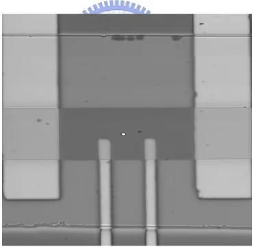
A cross-sectional view and photographic plan view of pentacene OTFTs fabricated in this experiment is shown in Fig.3-1and Fig.3-2. The detail fabrication processes are as follows:
Step 1. Preparation of Substrates
A p-type, single crystal silicon wafer (100) was used as the substrate and the gate electrode. After RCA cleaning, a 1000Å thermally-grown SiO2 layer was deposited
by furnace. After the SiO2 deposition, we try to remove the SiO2 layer from the
wafer of unpolished-side. The etching-solution we used is buffered oxide etching (B.O.E.). Hence, the wafer of unpolished-side without SiO2 layer can serve as a
gate-electrode. Finally, the substrate was cleaned in ultrasonic tank by the sequence of: de-ionic water (5 minutes), acetone (1 minutes), and de-ionic water (5 minutes).
Step 2. Spin-coated PMMA on SiO2
After substrate cleaning, we spin the solution-based Polymethylmethacrylate (PMMA) onto the substrate to modify the surface. The content of solution-based PMMA is a mix of PMMA and anisole with a concentration (10%) .Consequently, we
try to remove the residual solvent. The substrate is then baked on hot-plate at 90℃ about 30 minutes.
Step.3 Growth of Pentacene film and Electrodes
The pentacene powder used in this experiment was obtained from Aldrich and its purity was about 99%. The deposition of pentacene film is started at a pressure around 1×10⁻⁶ torr. The deposition-rate is controlled at ~0.5Å/sec and the thickness of
pentacene film was about 100nm, monitored by the quartz crystal oscillator. The pentacene film region is defined through the shadow-mask and the substrate temperature is controlled at room temperature(RT) during the pentacene film deposition.
After the pentacene deposition, a 100-nm-thick gold (Au) layer was deposited through shadow masks to serve as source/drain electrodes. The channel width (W) and length (L) of the Gated-four-probed OTFTs were 800μm and 1200μm, respectively.
Step.4 Passivation layer deposition
The NPB film was then deposited on the top of the device by thermal evaporation at room temperature (RT) at a pressure around 1×10⁻⁶ torr to a film
thickness of about 600 nm. Afterward, by using e-gun evaporation system, the multiple thin-film layers, which made by oxide(100nm) and metal(100nm) layers, can be continuously deposited on the NPB film at a pressure around 3×10⁻⁶ torr .
Finally , we spin the PDMS onto the device to passiviate the OTFTs. The substrate is then baked on hot-plate at 50℃ about 90 minutes.
The current-voltage (I-V) characteristics of our pentacene OTFTs were obtained from the semiconductor parameter analyzer Keithley 4200-SCS and Keithley 2636 in the dark at room temperature(RT).
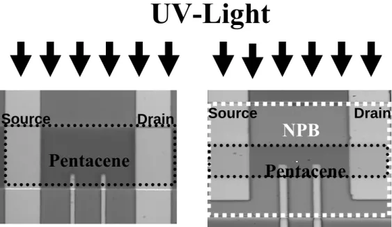
3-2 UV illumination experiments
In Figure.3-3 , we show the image of UV illumination experiments. The UV (Jelight Company, GLS-144 UV Lamp) illumination experiments were performed with un-passivated and passivated pentacene OTFTs under a strong UV (175-254 nm) with an optical power density of 0.043mW/cm2.The UV light was continuously
illuminated onto our un-passivated and passivated pentacene OTFTs for periods of 0, 10, 20, 40, 80, and 120 minutes.
Fig. 3-1 The device structure of pentacene OTFTs with NPB passivation layer
UV-Light
Fig. 3-3 The image of UV illumination experiments.
Pentacene
Source
Drain
NPB
Drain
Source
Pentacene
Chapter 4
Result and Discussion
4-1 Degradation of pentacene OTFTs under UV-light
illumination
In this experiment, we try to investigate that UV-light induced degradation on OTFTs and by the gated-4-probes OTFTs, the organic film properties and mental-contact effects can be studied separately. Moreover, it is conjected from material analysis to find what may be the dominative factor that influenced OTFT’s properties
4-1-1 Electrical properties of un-passivated OTFTs under
UV-light illumination
First , the figures. 4-1 show the transfer characteristics of un-passivated OTFTs under UV-light illumination. After about 120 minutes UV-light illumination, the turn-on current (ID) at VG= -45V of un-passivated OTFTs was significantly reduced
from 0.38 μA to 0.028 μA. It is clear that un-passivated OTFTs almost lost the drain current .
These UV-light illuminations effects are again observed from the plots of ID vs
hole mobilities, threshold voltage, subthreshold swing, and on/off current ratios, respectively. After about 120 minutes UV-light illumination , the pentacene OTFTs without the passivation layers exhibited significantly reduced in field effect mobility from 0.47 cm2 /V s to 0.039 cm2 /V s; the threshold voltage was significantly changed
from -12.2V s to -16.2V ; the subthreshold swing was significantly changed from 2.36 V/decade s to 4.78 V/decade ; the on/off current ratio was significantly reduced from 106 to103 when the off current was defined at V
GS = 0 V.
It is evident that the degradation of un-passivated OTFTs was significantly reduced under high energy UV-light illumination.
4-1-2 Electrical properties of Gated-Four-Probes on un-passivated
OTFTs under UV-light illumination
From potential-probes on channel, the voltage-drops at the source electrode (Δ ), drain electrode (VS ΔVD), and within the pentacene film (ΔVfilm ) can be
estimated by: 2 1 1 1 2 1 ( ) [ ] ( ) S S V V V V L V L L − Δ = − ⋅ − − 2 1 2 2 2 1 ( ) [ ( )] ( ) D D V V V V V L L L L − Δ = − + ⋅ − − 2 1 2 1 ( ) ( ) film V V V L L L − Δ = ⋅ − 1
electrode) and second potential probe (near the drain electrode), respectively. L 1
and L is the distance from the first potential probe to source electrode and the 2
second potential probe to drain electrode. L is the channel length.V and D V is the S
drain voltage and source voltage, respectively. The total contact resistance (Rcont)
and film resistance (Rfilm) can also be estimate by:
S D cont D V V R I Δ + Δ = film film D V R I Δ =
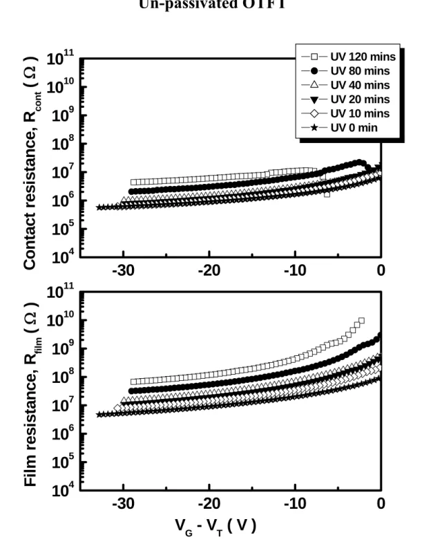
As shown in Fig. 4-2 , we show the he contact resistance and pentacene resistance by the gated-four-probes of un-passivated OTFT under UV-light illumination. When the UV-light illumination times increases, both the Rcont and the Rfilm will increase.
To study the effects of UV-light illumination on OTFT devices, the △Rcont
and △Rfilm is further plotted as a function of UV-light illumination times at G th
V −V = -25 V in Fig 4-3(a). After about 120 minutes UV-light illumination, the
cont
R will approach a maximum value about 4.9×10⁶ Ω, which is smaller than the
value of Rfilm around 8.1×10⁷ Ω. The Fig. 4-3(b) shows the percentage (%) of cont
R and Rfilm versus UV-light illumination times, respectively. It is clear that the
percentage (%) of Rfilm is as high as about 90% under different UV-light
illumination times. Thus, the OTFT characteristics should be mainly dominated by the pentacene film properties rather than the contact properties.
4-1-3 Material analysis on pentacene-OTFTs
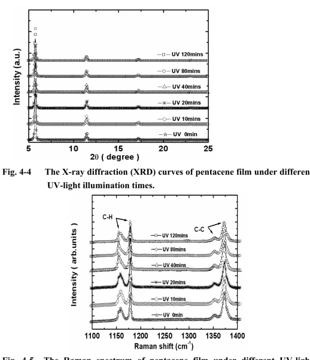
From the the transfer characteristics of pentacene OTFTs under UV-light illumination , it is important to discuss the degradation of UV-light illumination on OTFTs. Therefore , we try to investigate the pentacene film properties under different UV-light illumination times firstly. In Fig. 4-4 , we show the x-ray diffraction (XRD) curves of pentacene film under different UV-light illumination times. All pentacene films show the (001) signal with a peak value about 5.73° (degree). The higher order signal of (002) and (003) peak is also observed with a values about 11.47° (degree) and 17.21° (degree), respectively. According to the XRD analysis[47], it implies that the pentacene films under different UV-light illumination times are almost identical. It is clear that pentacene crystallization was not significantly changed after UV-light illumination. Consequently, we also try to verify the pentacene film by the Raman spectrum. With the Raman spectrum analysis, the conformational transition during carrier transport [47]. The pentacene vibration-modes of C−H (around 1155-1179cm-1) and C−C (around
1353-1380cm-1) bindings are plotted in Fig. 4-5 . According to the Raman spectrum analysis, the result also reveals that the intermolecular coupling was not be changed even if the pentacene films under different UV-light illumination times. Finally, we also show fourier transform infrared spectroscopy (FTIR) spectrum of the pentacene
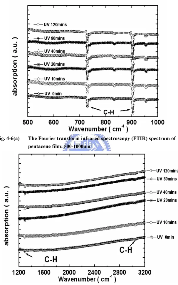
films under different UV-light illumination times. The FTIR spectrum of 100nm thick pentacene films on SiO2 (see Fig. 4-6 ) displays a number of strong absorption bands, which can be identified according to the literature [12,48]: 729 cm-1 and 903
cm-1 are out-of-plane C−H bending modes, 1296 cm-1 a ring stretching mode, and
3004 cm-1correspond to C−H in-plane stretching modes. According to the FTIR
spectrum analysis, the bonding of pentacene films was not be changed even if the pentacene films under different UV-light illumination times. Based on these material analysis, the crystalline, molecular coupling, and the absorptive properties of pentacene film under different UV-light illumination times should be almost identical. It is clear that deep UV do not damage the pentacene crystalline channel layer from the surface to the channel/gate oxide interface, and not generating excessive defects in the whole layer thickness.
In order to study the effect of UV-light illumination on OTFTs, we verified the effects of UV-light illumination on thin-film properties. In Fig. 4-7, we show the AFM images of pentacene films under different UV-light illumination times. Before illumination, the dendritic pentacene grains could be observed. Beside, the monolayer edges also clearly appeared. However, after illumination, several knobs appeared on the dendritic pentacene grains[12].The monolayer edges were blurred. Pentacene
UV cause a surface damage of organic pentacene which UV-light illumination times increases.
It is not clearly understood why UV cause a degradation of pentacene TFTs. However , it is conjectured from electron Spectroscopy for Chemical Analysis (ESCA) was used to examine the changes of thin film chemical bonding. The pentacene vibration-modes of carbon (C) signal (around 285eV) and oxygen (O) signal (around 532eV) bindings are plotted in Fig. 4-8(a). The carbon (C) signal of pentacene films is further plotted as a function of binding energy in Fig. 4-8(b), which were illuminated by UV-light with different times. Significantly, the carbon signal significantly decreased, additionally, a carbon-oxygen (O) related signal around 290eV appear after UV-light illumination[49]. We also show the oxygen signal in Fig. 4-8 (c).We found pentacene film without UV-light illumination showed a very low oxygen signal. However, when pentacene film was exposed to UV-light illumination, the oxygen signal significantly increased. This implied that UV-light illumination may result in a photo-induced oxidation of organic pentacene. This will result in changed bonding between the benzene ring and oxygen. The added oxygen in the pentacene film severely influenced OTFT performance.
To further find where the photo-induced oxidation of organic pentacene is, electron Spectroscopy for Chemical Analysis (ESCA) depth profile was plotted in Fig.
4-9. We can compare the carbon (C) signal and oxygen (O) signal, which were illuminated by UV-light with different times. Significantly, in the thickness of pentacene film thiner than 10 nm , the carbon signal significantly decreased. In contrast , the oxygen signal significantly increased. It is clear that UV-light illumination cause a surface oxidation of organic pentacene , generating deep level defects near the surface in the vicinity of oxygen molecules in air.[13]
According to charge transport mechanisms of pentacene OTFTs[50], all the charge of the conducting channel resides in the first monolayer next to the insulator–pentacene interface; in other words, the charges located close to the interface have the highest mobility, which reinforces their contribution to the conductivity of the conducting channel. Consequently, the conventional field-effect mobility gives a relatively good estimate for the actual mobility at the interface. However , the electron Spectroscopy for Chemical Analysis (ESCA) depth profile result further verify surface oxidation of pentacene film severely degraded OTFT performance.Therfore , it is clear that the charge of the conducting channel not just located in the first monolayer next to the insulator–pentacene interface ,but also in whole pentacene layer.
4-2 Ultraviolet light protective layer for OTFTs passivation
In order to protect the organic thin-film transistors (OTFTs) from degradation under UV-light illumination , we proposed on the passivation of pentacene TFTs using two kinds of passivation layers : TiO2, N′-bis(naphthalen-1-y)-N,N′-bis(phenyl) benzidine (NPB)/Mg/TiO2/PDMS and NPB.
For UV-light illumination , the TiO2 thin film have strong absorption property. Therefore , we used the TiO2 thin film to protect the organic thin-film transistors (OTFTs) from degradation under UV-light illumination. However, in figure 4-10(a) ,we shows the performance of the OTFT before and after the passivation with TiO2 . It is clear that there is a significant increment in the off-current after the
passivation. We signifies that UV-light illumination on the TiO2 thin film, occurring
the chemical reactions in TiO2 thin film. Furthermore, during the deposition process , x rays, and electron beams damages the pentacene active layer, resulting in the degradation of the field-effect mobility from 0.38 to 0.32 cm2/V.s, This result
coincides with the previous report on the X-rays and electron beams effect on pentacene OTFT.[45-46]
Therefore , in order to avoid OTFT degradation during the passivation process and the off current decrease, we proposed on the passivation of pentacene TFTs with NPB/Mg/TiO2/PDMS. By using e-gun evaporation system, the multiple thin-film
layers, which made by oxide and metal layers, can be continuously deposited on OTFTs. These multiple thin-film layers were low optical transparency and high gaseous resistance, which will act as the protective layers to avoid OTFT degradation under UV-light (wavelength: 175-254 nm) soaking. However , in figure 4-10(b) ,we shows the performance of the OTFT before and after the passivation with NPB/Mg/TiO2 /PDMS. It is clear that although the off-current does not change after
the passivation. But during the deposition process , X-rays, and electron beams damages the pentacene active layer[45-46], resulting in the degradation of the field-effect mobility from 0.44 to 0.35 cm2/V.s, so that the drop was 0.09 cm2/V s.
Therefore , in order to avoid OTFT degradation during the passivation process , we proposed the NPB film as the passivation for pentacene TFTs .Because the NPB film have highly transparent property.[51]. Furthermore , in figure 4-10(c) , we shows the transfer characteristics of the OTFT before and after passivation with NPB layer. Before passivation , the device shows a mobility about 0.47cm2/v-sec, a threshold
voltage about -12.2V, a subthreshold swing about 2.36 V/decade , and a on/off ratio about 106 . On the other hand, the OTFTs with NPB passivation show a similar
mobility about 0.48 cm2/v-sec, a lower threshold voltage about -11 V, a larger
subthreshold swing about 2.4V/decade, and a lower on/off ratio about 104. It is
subthreshold swing will be increased , and the on/off ratio will be reduced . But the field effect mobilities almost remains unchanged..Therefore , it is clear that during the passivation process , the NPB film does not damage on organic pentacene layer.
The transfer characteristics of the OTFTs before and after passivation with TiO2 ,NPB, NPB/Mg/TiO2/PDMS layers compared with literatures which have
summarized in Table 2. It is clear that the transfer characteristics of the OTFTs before and after passivation with NPB layer almost remains unchanged. This result for passsivation layer of pentacene OTFTs is our unique finding .Therefore, the NPB film as the passivation layer to protect the organic thin-film transistors (OTFTs) from degradation under UV-light illumination.
4-2-1 Transmittance and absorbing property of NPB passivation
To verify the UV protective properties of the NPB passivation , the transparent and absorptive properties are important demands. In this experiment, the NPB film with thickness about 600 nm was deposited on guartz glass by thermal evaporation , the spectrum of the film presented in Figure 4-11(a) and Figure 4-11(b) , respectively. During the visible wavelength of the spectrum , the NPB film displays a transmittance about as high as 80%, and based on the plot of the squared angular frequencyabsorption coefficient (α ω2 2) vs. photon energy (ev) ,the estimated optical bandgap of NPB film was around 2.9 eV[10]. It is clear that the NPB film is highly transparent[51]. It should be a good passivative layer for covering the OTFTs,
especially for in the application of displays.
4-2-2 Electrical properties of passivated OTFTs under UV-light
illumination
In Figures. 4-12 , we show the transfer characteristics of passivated OTFTs under UV-light illumination.After about 120 minutes UV-light illumination, the turn-on current (ID) at VG= -45V of un-passivated OTFTs was slightly changed from 0.4 μA
to 0.23 μA. It is clear that passivated OTFTs still showed a high current level of 0.23 μA while the un-passivated one almost lost the drain current (that decreased from 0.38 μA to less than 0.028 μA)
These UV illuminations effects are again observed from the plots of ID vs VG and
Log10 ID vs VG as presented in Fig. 4-12, where we can evaluate the field effect hole
mobilities, threshold voltage, subthreshold swing, and on/off current ratios, respectively. After about 120 minutes UV-light illumination , the pentacene OTFTs with the passivation layers exhibited slightly reduced in field effect mobility from 0.48 cm2 /V s to 0.30 cm2 /V s; the threshold voltage was slightly changed from -11V
to -12V ; the subthreshold swing was slightly changed from 2.40V/decade to 3.96 V/decade ; the on/off current ratio was slightly reduced from 104 to103 when the off
current was defined at VGS = 0 V. Evidently, with NPB passivation, the UV light
induced degradation was reduced.
4-2-3 Electrical properties of Gated-Four-Probes on NPB-passivated
OTFTs under UV-light illumination
In Figures. 4-13 , we show the he contact resistance and pentacene resistance by the gated-four-probes of passivated OTFT under UV-light illumination, respectively. When the UV-light illumination times increases , both the Rcont and the Rfilm will
slightly increase. It is clear that the NPB film will protected pentacene OTFTs effectively from high energy UV illumination
4-3 Comparison of un-passivated OTFTs and
NPB-passivated OTFTs under UV-light illumination
4-3-1 Electrical properties of un-passivated OTFTs and
NPB-passivated OTFTs under UV illumination
The field effect mobility vs UV illumination period plotted and summarized in Fig. 4-14(a). The field-effect mobility of un-passivated OTFTs significantly degraded from 0.47 cm2 /V s to 0.04 cm2 /V s while the NPB passivated one does slightly
degrade from 0.48 cm2 /V s to 0.30 cm2 /V s. The NPB-passivated TFT shows a
gradual degradation of mobility while the un-passivated one does very rapid degradation. .Similar results were reported with SnO2 thin film.(See Fig.4-14(b)).
In Figures. 4-15 presents the variation of the linear regime threshold voltage, under different UV-light illumination times. The relative change from -12.2V s to -16.2V in the threshold voltage of un-passivated OTFTs, as the UV-light illumination times are increased, are much larger than the relative change ( from -11V s to -12V) in the NPB-passivated OTFTs, as stated above.
It is evident that the NPB film have protected pentacene OTFTs effectively from high energy UV illumination
4-3-2 Electrical properties of Gated-Four-Probes un-passivated
OTFTs and Gated-Four-Probes passivated OTFTs under UV
illumination
As shown in Fig. 4-16 , the Rcont and the Rfilm is plotted as a function of
gate-voltage minus threshold-voltage (VG−Vth= -25 V) of un-passivated OTFTs and
passivated OTFTs under UV-light illumination , respectively. When the UV-light illumination times increases , both the Rcont and the Rfilm will increase. But the
cont
R and the Rfilm of un-passivated OTFTs shows a significantly increases while
the NPB passivated one does slightly increase .It is clear that the NPB film will protected pentacene OTFTs effectively from high energy UV illumination.
10
-1310
-1210
-1110
-1010
-910
-810
-710
-6-50
-40
-30
-20
-10
0
0.0
1.0x10
-72.0x10
-73.0x10
-74.0x10
-75.0x10
-76.0x10
-7 UV 120mins UV 80mins UV 40mins UV 20mins UV 10mins UV 0 minD
rai
n cur
re
nt
(
A
)
VD=-2V
Gate Voltage(V)
D
rai
n cur
rent
(
A
)
Fig.4-1 The transfer characteristics of pentacene OTFTs without NPB passivation layer under different UV-light illumination times
Un-passivated OTFT
-30
-20
-10
0
10
410
510
610
710
810
910
1010
11-30
-20
-10
0
10
410
510
610
710
810
910
1010
11F
ilm
r
e
s
is
ta
n
c
e
, R
film(
Ω
)
V
G- V
T( V )
C
o
nt
act
r
e
si
st
ance,
R
cont(
Ω
)
UV 120 mins UV 80 mins UV 40 mins UV 20 mins UV 10 mins UV 0 minFig. 4-2 The variation of the linear regime resistance of un-passivated under different UV-light illumination times
0 2 0 4 0 6 0 8 0 1 0 0 1 2 0 0 1 x 1 07 2 x 1 07 3 x 1 07 4 x 1 07 5 x 1 07 6 x 1 07 7 x 1 07 8 x 1 07 9 x 1 07 1 x 1 08 0 1 x 1 07 2 x 1 07 3 x 1 07 4 x 1 07 5 x 1 07 6 x 1 07 7 x 1 07 8 x 1 07 9 x 1 07 1 x 1 08 Δ
R
c ΔR
f ilm ΔR
film(
Ω)
ΔR
c(
Ω)
VD= - 2 V VG- VT H= - 2 5 V U V illu m in a t io n t im e ( m in u t e s )Fig. 4-3(a) The △Rcont and △Rfilm is plotted as a function of UV-light
illumination times. 0 2 0 4 0 6 0 8 0 1 0 0 1 2 0 0 1 0 2 0 3 0 4 0 5 0 6 0 7 0 8 0 9 0 1 0 0 % 1 0 0 % % 1 0 0 % f i l m f i l m f i l m c o n t c o n t c o n t f i l m c o n t R R R R R R R R = × + = × + VD= - 2 V V G- VT H= - 2 5 V R f i l m % R c o n t % R esi st anc e ( % ) U V i l l u m i n a t i o n t i m e ( m i n u t e s )
Fig. 4-4 The X-ray diffraction (XRD) curves of pentacene film under different UV-light illumination times.
Fig. 4-5 The Raman spectrum of pentacene film under different UV-light illumination times
Fig. 4-6(a) The Fourier transform infrared spectroscopy (FTIR) spectrum of pentacene film: 500-1000nm
Fig. 4-6(b) The Fourier transform infrared spectroscopy (FTIR) spectrum of pentacene film:1200nm-3200nm
(a) UV 0 min (b) UV 10 mins
(c) UV 20 min (d) UV 40 mins
(e) UV 80 min (f) UV 120 mins
Fig. 4-7 The AFM images of pentacene films under different UV-light illumination times are shown in Fig. (a) ,. (b) , (c) , (d) ,(e) ,and (f).
Monolayer edges
Fig. 4-8(a) Electron Spectroscopy for Chemical Analysis (ESCA) under different UV-light illumination times : Oxygen (O1s) and Carbon (C 1s)
2 8 0 2 8 5 2 9 0 2 9 5 C - O C C 1 S B i n d i n g e n e r g y ( e V ) In te n s ity ( a .u . ) U V 1 2 0 m i n s U V 8 0 m in s U V 4 0 m in s U V 2 0 m in s U V 1 0 m in s U V 0 m i n
Fig. 4-8(b) Electron Spectroscopy for Chemical Analysis (ESCA) under different UV-light illumination times :Carbon (C 1s)
5 2 5 5 3 0 5 3 5 5 4 0 B i n d i n g e n e r g y ( e V ) O O 1 S In te nsi ty ( a. u. ) U V 1 2 0 m in s U V 8 0 m in s U V 4 0 m in s U V 2 0 m in s U V 1 0 m in s U V 0 m in
Fig. 4-8(c) Electron Spectroscopy for Chemical Analysis (ESCA) under different UV-light illumination times : Oxygen (O 1s)
0 20 40 60 80 100 O 1S C 1S In te n s it y ( a .u . ) thickness ( nm ) O-UV 0min O-UV 40mins O-UV 120mins C-UV 0min C-UV 40mins C-UV 120mins
Fig. 4-9 Electron Spectroscopy for Chemical Analysis (ESCA) of depth profile under different UV-light illumination times
10-13 10-12 10-11 10-10 10-9 10-8 10-7 10-6 10-5 -50 -40 -30 -20 -10 0 0.0 2.0x10⁻⁷ 4.0x10⁻⁷ 6.0x10⁻⁷ 8.0x10⁻⁷ 1.0x10⁻⁶ VD = -5V after passivation befoe passivation D rai n cu rr en t ( A ) D ra in cu rr en t ( A ) Gate Voltage(V)
Fig. 4-10(a) The performance of the OTFT before and after the passivation with TiO2 10-13 10-12 10-11 10-10 10-9 10-8 10-7 10-6 10-5 -50 -40 -30 -20 -10 0 0.0 2.0x10⁻⁷ 4.0x10⁻⁷ 6.0x10⁻⁷ 8.0x10⁻⁷ 1.0x10⁻⁶ VD = -5V after passivation before passivation D rai n cur rent ( A ) D rai n cur rent ( A ) Gate Voltage(V)
Fig. 4-10(b) The performance of the OTFT before and after the passivation with NPB/Mg/TiO /PDMS
10-13 10-12 10-11 10-10 10-9 10-8 10-7 10-6 -50 -40 -30 -20 -10 0 0.0 1.0x10⁻⁷ 2.0x10⁻⁷ 3.0x10⁻⁷ 4.0x10⁻⁷ 5.0x10⁻⁷ VD = -2V NPB passivation without NPB passivation Dr ai n cur rent ( A ) Dr ai n cur rent ( A ) Gate Voltage(V)
Fig. 4-10(c) The performance of the OTFT before and after the passivation with NPB
200 300 400 500 600 700 800 0 20 40 60 80 100
Thermally evaporated NPB film Thickness : ~ 600nm T ransm it ta nce( % ) Wavelength(nm)
Fig. 4-11(a) The transmission curve of NPB film (600nm) was plotted as a function of wavelength
Fig. 4-11(b) The absorption spectrum of NPB fim was plotted as a function of
-50
-40
-30
-20
-10
0
10
-1310
-1210
-1110
-1010
-910
-810
-710
-60.0
1.0x10
-72.0x10
-73.0x10
-74.0x10
-75.0x10
-76.0x10
-7D
rai
n cu
rr
en
t (
A
)
Gate Voltage(V)
UV 120mins UV 80mins UV 40mins UV 20mins UV 10mins UV 0 minV
D= -2V
D
rai
n cur
rent
(
A
)
Fig. 4-12 The transfer characteristics of pentacene OTFTs with NPB passivation layer under different UV-light illumination times