國立交通大學
電子工程學系 電子研究所碩士班
碩 士 論 文
以深層暫態能譜分析碳化矽缺陷
之研究暨溝槽式接面蕭基位障二
極體之設計分析
A study on the Defect in SiC by Deep Level
Transient Spectroscopy (DLTS) and Design
Analysis of the SiC Trench Junction Schottky
Barrier (TJBS) Diode
研究生:連崇德
指導教授:崔秉鉞 教授
以深層暫態能譜分析碳化矽缺陷之研究暨溝槽
式接面蕭基位障二極體之設計分析
A study on the Defect in SiC by Deep Level
Transient Spectroscopy (DLTS) and Design
Analysis of the SiC Trench Junction Schottky
Barrier (TJBS) Diode
研究生:連崇德 Student : Chong-De Lien
指導教授:崔秉鉞 Advisor : Bing-Yue Tsui
國立交通大學 電子工程學系 電子研究所
碩士論文
A Thesis
Submitted to Department of Electronics Engineering & Institute of Electronics College of Electrical and Computer Engineering
National Chiao Tung University in Partial Fulfillment of the Requirement
for the Degree of Master of Science in
Electronic Engineering 2013
Hsinchu, Taiwan, Republic of China 中華民國一 O 二年九月
i
以深層暫態能譜分析碳化矽缺陷之研究暨溝槽
式接面蕭基位障二極體之設計分析
研究生:連崇德 指導教授:崔秉鉞
國立交通大學電子工程系 電子研究所碩士班
摘要
由於碳化矽具有高崩潰電場和高導熱係數,應用於高溫高壓的元件是非常好 的半導體材料。對於高壓元件而言,磊晶層的品質會影響到導通電阻、崩潰電壓 和逆偏漏電,所以是非常重要的一環。深層暫態能譜分析能夠測量出缺陷能階、 捕獲截面積,以及缺陷密度。此外,深層暫態能譜分析對於缺陷擁有高靈敏度, 而且與其它偵測系統比起來相對容易去架設,因此我們選擇深層暫態能譜分析來 偵測磊晶層之中的缺陷。而碳化矽中最廣泛的高壓元件應用就是蕭基位障二極體、 接面二極體和接面蕭基位障二極體。為了改進接面蕭基位障二極體的特性或是簡 化製程,有許多不同的結構變化。溝槽式接面蕭基位障二極體是當中最新的結構, 因此我們將會利用Sentaurus TCAD tool,對於溝槽式接面蕭基位障二極體去找出 其設計概要。 深層暫態能譜分析的架設是利用安捷倫半導體儀器分析儀和有溫度控制器 的探測台。利用市售之深層暫態能譜分析系統來作為我們深層暫態能譜分析之系 統驗證。我們的系統與市售系統在相同位置有一樣的峰值,只是我們的半導體儀 器分析儀的電容量測速度比較慢,所以我們的系統有著相對弱的訊號。 試片方面製作了鎳金屬於碳化矽上的蕭基位障二極體和電容去量測磊晶層 的缺陷。對於蕭基二極體而言,深層暫態能譜分析系統沒有量測到任何的缺陷。 因此利用低劑量之氮離子佈值去創造缺陷。經過離子佈值之後,有非常強烈的深ii 層暫態能譜訊號被偵測到,但是這訊號是由不同缺陷組成的,所以無法萃取缺陷 能階。我們也利用不同的方式去減少離子佈值造成的缺陷,當中最有效的是 1600 度的高溫退火,幾乎所有離子佈值造成的缺陷都可以被修復,只是高溫退火同時 也會產生缺陷 Z1/2,而缺陷 Z1/2可以利用高溫退火前之碳離子佈值,或是碳化矽 之氧化去消除。 在本次研究中,我們也使用深層暫態能譜分析系統去量測碳化矽電容之介面 能態。而電容的介電層是利用熱氧化方式生長在碳化矽上的二氧化矽。而電容量 測到的深層暫態能譜並不是介面能態,反而是被介電層缺陷所主導整個分析。若 是深層暫態能譜量測到含有其他種缺陷,那麼利用深層暫態能譜萃取出之介面能 態將會是不正確的。而利用離子佈值後的磊晶層所做出之電容,展現了非常差的 電容對電壓曲線,但是在深層暫態能譜分析方面卻與蕭基位障接面二極體有一樣 的結果。 溝槽式接面蕭基位障二極體之模擬分析已經利用不同的布局參數去找到它 的設計概要。當溝槽之深度加深時,因為從側壁來的額外電流,所以有比較小的 臨界電壓。轉換電壓被定義成電流導通機制由單極電流 (蕭基接面電流) 轉換成 雙極電流 (介面二極體電流)的電壓。與一般接面蕭基二極體相比,溝槽式接面 蕭基位障二極體有比較低的轉換電壓,且導通之後有相對低的導通電阻和比較的 順向導通電流。轉換電壓會隨著蕭基接面的寬度增加而增加,但是會隨著接面二 極體之寬度和溝槽深度而減少。 與一般接面蕭基位障二極體相比,由於溝槽式接面蕭基位障二極體有溝槽底 部有溝槽角落和較薄的磊晶層,所以會有比較低的崩潰電壓。而對於溝槽式接面 蕭基位障二極體而言,崩潰發生的原因是來自於結構上的設計,因此並不能用邊 緣終端技術來提高它的崩潰電壓。溝槽式接面蕭基位障二極體比較適合應用在高 電流之元件應用,然而一般接面蕭基位障二極體卻是比較適合應用在高壓操作使 用。
iii 總體而言,深層暫態能譜分析系統之架設與驗證已經完成。因為氮離子佈值 所造成的不同缺陷已經被偵測到,而且這些缺陷可以藉由 1600 度的退火去除, 但是同時也會產生缺陷 Z1/2。深層暫態能譜分析於碳化矽電容上量到的訊號主要 是介電層缺陷所主導;若是深層暫態能譜量到有其他缺陷,那麼在轉換至介面能 態時,介面能態將會被高估。在相同條件下,蕭基位障二極體與電容有一樣的深 層暫態能譜。溝槽式接面蕭基位障二極體的設計概要已經被分析出來,而溝槽結 構會對元件的所有特性造成影響。溝槽式接面蕭基位障二極體比較適合應用在高 電流之元件應用,然而一般接面蕭基位障二極體卻是比較適合應用在高壓操作使 用。
iv
A study on the Defects in SiC by Deep Level
Transient Spectroscopy (DLTS) and Design
Analysis of the SiC Trench Junction Schottky
Barrier (TJBS) Diode
Student: Chong-De Lien Advisor: Bing-Yue Tsui
Department of Electronics Engineering
Institute of Electronics
National Chiao Tung University
Abstract
Silicon carbide (SiC) is an ideal semiconductor material for the higher power and high temperature applications due to its wide bandgap, high critical electric field, and good thermal conductivity. For high breakdown voltage device, the quality of the n -epi-layers is very important, because it influences the on-resistance, junction leakage current, and breakdown voltage of device. Deep level transient spectroscopy (DLTS) is capable of characterizing the defect energy, defect capture cross section, and density of defect quantitatively. Besides, DLTS has high sensitivity and is relatively easier than the other defect detection systems to be setup. Hence, we choose DLTS to analysis the defects in the epi-layer. The widest applications of SiC are its power diodes like Schottky barrier diode, pn diode, and junction barrier Schottky (JBS) diode. The JBS diodes have many different variations of structure for the improvement in performance or the ease of process. The trench junction barrier Schottky (TJBS) diode is one of the latest innovations, so we are going to figure out
v
the design guidelines of the TJBS diodes by the Sentaurus TCAD tool.
The setup of DLTS system consists of a semiconductor parameter analyzer with a capacitance measurement unit and a probe station with a temperature heating controller. Our DLTS system can measure the same signal but weaker signal intensity in comparison with the commercial DLTS system due to the sampling rate limitation of the capacitance measurement unit.
To measure the defects in epi-layer, Ni/SiC Schottky barrier diode and SiC MOS capacitor are fabricated. For the Schottky barrier diode, there is no defect measured by our DLTS system. In order to create defects in the epi-layers, low dose nitrogen ion implantation is introduced. After ion implantation, strong signal is measured in the DLTS, but severe overlap of signals from different defects makes it hard to extract the defect energy. Different processes are applied to eliminate the defects induced by ion implantation. The most effective one is annealing at 1600 oC.Almost all the defects induced by ion implantation are eliminated. However, high temperature annealing could generate Z1/2 defect.
The interface state of the SiC MOS capacitor is also investigated by our DLTS system. The gate dielectric of MOS capacitor is thermal oxide. The DLTS of MOS capacitor is dominated by oxide trap in SiO2. The signals from oxide traps overlap the
signals from interface states. If the DLTS is not only composed of interface states, the direct transformation of DLTS into interface state density would be incorrect. For MOS capacitor fabricated on the ion-implanted epi-layer, poor capacitance-voltage characteristic is exhibited, but the DLTS result is the same as that measured on the Schottky barrier diode.
The design guidelines of the TJBS diode have been investigated by considering different geometric parameters. As the trench depth becomes deeper, the cut-in voltage becomes slight lower due to the extra sidewall current. We define the
vi
transition voltage as the voltage at which the current transport changes from unipolar conduction (Schottky junction dominant) to bipolar conduction (pn junction dominant). TJBS diodes have lower transition voltage, and thus lower specific on-resistance and higher forward conduction current after bipolar conduction. The transition voltage increases as wider Schottky contact width, but decreases as wider pn junction width or deeper trench depth. Because of trench corner and thinner epi-layer under the pn junction due to the trench structure, relatively low breakdown voltage is observed on TJBS diodes than JBS diodes. For TJBS diodes, the breakdown voltage depends on structural design, which can be compensated by edge termination design.
In conclusion, the setup and verification of DLTS system have been accomplished. Different defects after nitrogen ion implantation has been detected in Schottky barrier diode. These defects can be annihilated by a 1600 oC annealing, but meanwhile Z1/2 defect will be generated. The DLTS of MOS capacitor are dominated
by oxide trap. The Dit from DLTS would be overestimated if other traps are mixed in
the signal. Under the same process condition, Schottky barrier diode has identical DLTS result to MOS capacitor. The design guidelines of TJBS diodes are proposed. The trench affects all the characteristics of device. It is suggested that TJBS diodes are suitable for the higher current application, while JBS didoes are favored for high voltage application.
vii
Contents
Abstract (Chinese)………..…. i
Abstract (English)……….……. iv
Contents………. .vii
List of Tables………ix
List of Figures………...x
Chapter 1 Introduction ……….……….…..1
1-1 History of Power Devices ………..…………....………….……1
1-2 Overview of Wide Band-gap Materials ……….…..……..………. 3
1-3 Silicon Carbide (SiC) Crystals………...……….….…….……...5
1-4 Quality of SiC epi-layer……...……….……….…..………....6
1-5 Power diodes of SiC ……….…….…….……….8
1-6 Thesis Organization……….……..………..……….9
Chapter 2 Defect
in
4H-SiC
by
deep
level
transient
spectroscopy ……….………...…...17
2-1 Introduction to deep level transient spectroscopy (DLTS)………..…….……….……...………..17
2-2 Setup of DLTS system………...……….…………..………….19
2-3 Verification of DLTS system……….….………..……….20
2-4 Sample fabrication for DLTS measurement….………..………...21
2-4.1 Ni/SiC Schottky barrier diode.…………...…..………...21
2-4.2 SiC MOS capacitor………….…………...…..………...21
2-5 Electrical characteristics of Ni/SiC Schottky barrier diode.….………….…...22
viii
2-5.2 Capacitance-voltage characteristics……….………..………...24
2-5.3 DLTS results of Ni/SiC Schottky barrier diode ………...24
2-6 Electrical characteristics of MOS capacitor.….………...26
2-6.1 Capacitance-voltage characteristics………...26
2-6.2 DLTS results of MOS capacitor ………....27
2-7 Summary of DLTS results……….….………...29
Chapter 3 Design Analysis of the SiC Trench Junction Schottky
Barrier (TJBS) Diode………..………..……….………55
3-1 Structure and parameters in simulation……….……...…………...…..55
3-2 Forward bias characteristics of JBS diode………..…...56
3-3 Forward bias characteristics of TJBS diode………..………….……....58
3-4 Comparison of electrical characteristics of TJBS diode………...……….……59
3-5 Summary of the TJBS diodes ……….……….………..………....…60
Chapter 4 Conclusions and Future Works………..…..….…...….…..76
4-1 Conclusions……… ….…….…………..……...…76
4-2 Future Works……….…….…………..…….….78
References……….…….……….………..……...80
ix
List of Tables
Chapter 1
Table1-1 Physical characteristics main wide bandgap semiconductor [11]………….10 Chapter 2
Table2-1 Specifications of C-t function in Agilent B1500A semiconductor device parameter analyzer [34]………...………..31. Table2-2 Main processes conditions of Ni/SiC Schottky barrier diodes.…………..…...31
Table2-3 Main processes conditions of SiC MOS capacitors.………..………...32
Table2-4 Measurement conditions in DLTS of Ni/SiC Schottky barrier diodes. Sample IA has different turn-on voltage, so the depletion width doesn’t change under the same DLTS measurement condition as the other……….32
Table 2-5 Measurement conditions in DLTS of SiC MOS capacitors. The VP is depend
on the VFB of each sample, and all the sample have the same electric
x
List of Figures
Chapter 1
Fig.1-1 In SiC, silicon atom is covalently bonded with 4 carbon atoms in the tetrahedral arrangement [13]………...………..………….10 Fig.1-2 Three possible suited positions for hexagonal structure [14]……….….….……….…………...….11 Fig.1-3 Common prototypes of SiC with different stacking orders [14]………..……….…………..12 Fig.1-4 Four Miller Indices (a1 a2 a3 c) in hexagonal structure
[14]………...………..13 Fig.1-5 Comparison of unipolar limit of specific on-resistance versus blocking voltage
for some device types in Si and SiC [15]……….13 Fig.1-6 Cross section schematic of VDMOSFET, UMOSFET, BJT, IGBT [16,
17].………..………...…….14 Fig.1-7 Cross section schematics of Schottky diode and PiN diode in vertical structure………...…..….…15 Fig.1-8 Cross section schematics of junction barrier diode (JBS). In forward bias, the Schottky contact will turn on at low voltage; in reverse bias, the p-type grids will deplete n-drift region to provide higher breakdown voltage and smaller leakage [28]………15 Fig. 1-9 Dual-metal trenched Schottky diode (DMTS) with two different metals to achieve and trenched MOS barrier Schottky diode (TMBS) with MOS structure are introduced by the same basic theory of JBS [28] ……….……16 Fig. 1-10 Device configuration of trenched junction barrier Schottky diode (TJBS)
xi
[30]. In forward bias, the Schottky contact will turn on at low voltage,and sidewall of schoottky diode can provide more on-current to lower down its on-resistance; in reverse bias, the p-type grids will deplete n-drift region to maintain breakdown voltage and smaller leakage………..16
Chapter 2
Fig. 2-1 Operation principle of DLTS: the dash line in depletion is defect………….33 Fig. 2-2 Extraction of transient capacitance with different temperatures. Select two
time points t = t1 and t = t2, so at proper temperature T1 the δC will be
maximum.………..….…………..………..….……… 33 Fig. 2-3 Capacitance-time-Temperature measurement flow: 1. Check the temperature
of chunk 2. Invoke C-t measurement……… 34 Fig. 2-4 “ln(τeT2) – 1/kT” plot. From the slope of regression line, we can get energy of
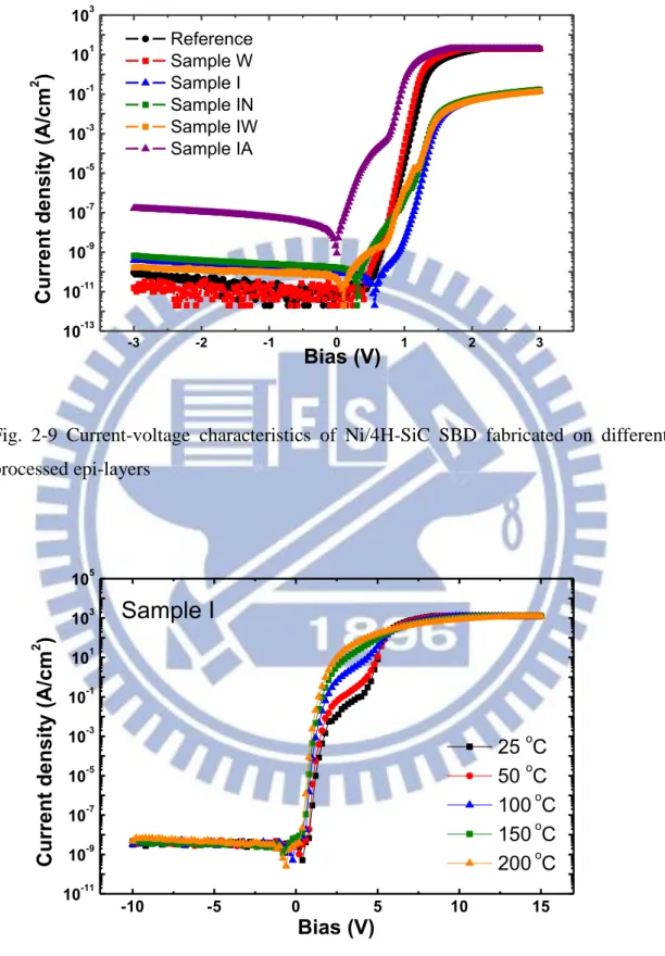
trap, and from the interception on y-axis, we can obtain the capture cross section. ……….34 Fig. 2-5 Measured DLTS of commercial DLTS system and our DLTS system…...…35 Fig. 2-6 Schematic of different sampling time has the same emission time constant..35 Fig. 2-7 Configuration of Ni/SiC Schottky barrier diode (SBD) …...…36 Fig. 2-8 Configuration of SiC MOS capacitor…...……….36 Fig. 2-9 Current-voltage characteristics of Ni/4H-SiC SBD fabricated on different
processed epi-layers………...…………37 Fig. 2-10 Current-voltage characteristics over temperature characteristics of
Ni/4H-SiC SBD sample I with ion implantation………37 Fig. 2-11 Current-voltage over temperature characteristics of Ni/4H-SiC SBD sample
IN with ion implantation and 1050 oC N2 annealing…………..………38
Fig. 2-12 Current-voltage over temperature characteristics of Ni/4H-SiC SBD sample IW with ion implantation and 1050 oC wet oxidation………..………..38
xii
Fig. 2-13 Cross section of sample I by TEM, and smooth morphology is observed...39
Fig. 2-14 Cross section of sample IA by TEM, and poor morphology is observed which is responding for phenomenon of double barrier and high reverse leakage current……….…………..39
Fig. 2-15 Capacitance-voltage characteristics of Ni/4H-SiC SBD fabricated on different processed epi-layers...40
Fig. 2-16 Extracted concentration by C-2-V characteristics of Ni/4H-SiC SBD sample IA. The slope reflects the donor concentration of epi-layer after dopant activation. ...40
Fig. 2-17 Measured DLTS result of Ni/4H-SiC SBD reference sample...41
Fig. 2-18 Measured DLTS result of Ni/4H-SiC SBD sample I...41
Fig. 2-19 Measured DLTS result of Ni/4H-SiC SBD sample W...42
Fig. 2-20 Measured DLTS result of Ni/4H-SiC SBD sample IN...42
Fig. 2-21 Measured DLTS result of Ni/4H-SiC SBD sample IW...43
Fig. 2-22 Measured DLTS result of Ni/4H-SiC SBD sample IA. ...43
Fig. 2-23 ln(τeT2) – 1/kT plot. Activation energy and capture cross section can be extracted from the slope and interception on y-axis...44
Fig. 2-24 High-low frequency C-V characteristics of SiC MOS capacitor sample W……….……...44
Fig. 2-25 High-low frequency C-V characteristics of SiC MOS capacitor sample P..……….……...45
Fig. 2-26 Different frequency C-V characteristics of SiC MOS capacitor sample IP..………...45
Fig. 2-27 High-low frequency C-V characteristics of SiC MOS capacitor sample IAP. ..………...……...46
xiii
Fig. 2-29 Equivalent circuit of MOS capacitor with highly resistive substrate [48]...47
Fig. 2-30 Simulation and experiment result of MOS capacitor with highly resistive substrate [48]………...……..………...……...47
Fig. 2-31 Capacitance-voltage characteristics over temperatures of SiC MOS capacitor sample W.……...……..………...……...48
Fig. 2-32 Capacitance-voltage characteristics over temperatures of SiC MOS capacitor sample P.……...……..………...……...48
Fig. 2-33 Capacitance-voltage characteristics over temperatures of SiC MOS capacitor sample IAP…...……..………...……...49
Fig. 2-34 Traps can be detected by DLTS system [50]...……...49
Fig. 2-35 Transient capacitance of two different mechanisms [50]...50
Fig. 2-36 Measured DLTS of SiC MOS capacitor sample W...50
Fig. 2-37 Measured Dit from of SiC MOS capacitor sample W...51
Fig. 2-38 Measured DLTS of SiC MOS capacitor sample P...51
Fig. 2-39 Measured Dit from of SiC MOS capacitor sample P...52
Fig. 2-40 Measured DLTS of SiC MOS capacitor sample I…...52
Fig. 2-41 Measured DLTS of SiC MOS capacitor sample I with larger reverse bias to observe the substrate defect with higher activation energy………53
Fig. 2-42 Measured DLTS of SiC MOS capacitor sample IAP………53
Fig. 2-43 Measured Dit from of SiC MOS capacitor sample IAP………54
Chapter 3 Fig. 3-1 Simulation structure and geometric parameters of JBS diode and TJBS diode………...…………62
Fig. 3-2 Simulated forward characteristics of JBS diode with Ws= 0.25 m and different values of Wp….………...…...…62
xiv
Fig. 3-3 Simulated forward characteristics of JBS diode with Ws= 0.5 m and different values of Wp..………...……...…63 Fig. 3-4 Simulated forward characteristics of JBS diode with Ws= 1 m and different values of Wp………….………...……...…63 Fig. 3-5 Simulated forward characteristics of JBS diode with Ws= 2 m and different values of Wp………….………...……...…64 Fig. 3-6 Simulated forward characteristics of JBS diode with Ws= 3 m and different values of Wp………….………...……...…64 Fig. 3-7 Simulated forward characteristics of JBS diode with Wp= 3 m and different values of Ws. ………….………...…..…...…65 Fig. 3-8 Relations of transition voltage with Wp and Ws in JBS diodes……….65 Fig. 3-9 Depletion region edge before and after the bipolar switch of smooth and discontinuous I-V curve……….66 Fig. 3-10 Electron current density and hole current density before and after the bipolar
switch of smooth and discontinuous I-V curve……….66 Fig. 3-11 Electrostatic potential at the pn junction near the Schottky contact before
and after the bipolar switch of smooth and discontinuity I-V curve. Different total electrostatic potential is due to different transition voltage of Ws= 0.25
m and 3 m………..………67
Fig. 3-12 Simulated forward characteristics of TJBS diode with D= 0.5 m, Ws= 0.25 m and different values of Wp………...……67 Fig. 3-13 Simulated forward characteristics of TJBS diode with D= 0.5 m, Ws= 0.5 m and different values of Wp………...……68 Fig. 3-14 Simulated forward characteristics of TJBS diode with D= 0.5 m, Ws= 1.0 m and different values of Wp. ………...……68 Fig. 3-15 Simulated forward characteristics of TJBS diode with D= 0.5 m, Ws= 2.0
xv
m and different values of Wp.………...……69 Fig. 3-16 Simulated forward characteristics of TJBS diode with D= 0.5 m, Ws= 3.0 m and different values of Wp.………...……69 Fig. 3-17 Simulated forward characteristics of TJBS diode with D= 0.5 m, Wp= 3.0 m and different values of Ws.………...……70 Fig. 3-18 Relations of transition voltage with Wp and Ws in TJBS diodes with D= 0.5
m……….………...……70
Fig. 3-19 Comparison of simulated forward characteristics of JBS diode and TJBS diodes with Ws= 0.25 m and Wp = 3 m………71 Fig. 3-20 Comparison of simulated forward characteristics of JBS diode and TJBS
diodes with Ws= 0. 5 m and Wp = 3 m.………71 Fig. 3-21 Comparison of simulated forward characteristics of JBS diode and TJBS
diodes with Ws= 1.0 m and Wp = 3 m…………..………72 Fig. 3-22 Comparison of simulated forward characteristics of JBS diode and TJBS
diodes with Ws= 2.0 m and Wp = 3 m…………..………...72 Fig. 3-23 Comparison of simulated forward characteristics of JBS diode and TJBS
diodes with Ws= 3.0 m and Wp = 3 m………..73 Fig. 3-24 Breakdown voltage of JBS diode with different parameters………73 Fig. 3-25 Breakdown voltage of TJBS diode with D= 0.5 m. and different parameters………..74 Fig. 3-26 Breakdown voltage of TJBS diode with D= 1 m. and different
parameters………..74 Fig. 3-27 Relations of different electrical characteristics with different parameters...75
1
Chapter 1
Introduction
1-1 History of Power Devices
The first power device is germanium diode appeared in 1952. In 1957, Silicon controlled rectifier (SCR) [1], also called thyristor, was invented in a 4-layer structure with alternating n-type layer and p-type layer. SCR has the advantages of high blocking voltage and high on-current. The structure of SCR contains 3 bipolar junctions. These junction capacitances result in low switching speed of about 50 to 60 Hz [2].
Bipolar Junction Transistor (BJT) was introduced in 1960s, which is capable of withstanding high reverse blocking voltage and high on-current. In the meanwhile, BJT overcomes the slow switching speed of SCR and can be controlled by external signal [3]. However, it still takes time to charge junction capacitances in BJT which slows the switching speed [4]. Furthermore, BJT has poor current gain in the high frequency applications [5].
With the mature of semiconductor process technology, the power MOSFET commercial products became available in 1970s. Power MOSFET has high input impendence and low input driving current. MOSFET has also much faster switching speed than BJT, because MOSFET is free of minority carrier storage phenomenon [3]. The main drawback of MOSFET is that it’s limited to lower power applications [6].
Insulated Gate Bipolar Transistor (IGBT) combines the advantages of BJT and MOSFET [3]. IGBT has the gate-structure of MOSFET and bipolar conduction of BJT, which can be controlled by external signal. Better conducting current and higher breakdown voltage than MOSFET can be achieved. However, if the switching speed
2
in IGBT become faster, the forward voltage drop will become larger. IGBT has slower switching speed than MOSFET, although this problem has been solved in recently researches [3].
Since the introduction of power device to today, it has been passed over several decades, and most of power devices are made of silicon. Many efforts have been devoted to meet the requirements of power devices, and the most important characteristics of power devices are high breakdown voltage, low on-resistance, low reverse leakage current, high operation temperature, and fast switching speed. The followings are the fundamentals of these characteristics:
1. Breakdown voltage
Impact ionization is the phenomenon that electron gain energy from semiconductor band bending. Once the electron energy reaches 1.5 times of the semiconductor bandgap [7], the electron can generate an electron-hole pair. The generated electron and hole gain energy from band-bending again, and induce another two electron-hole pairs. Such a multiplication process is called avalanche breakdown. 2. On–resistance (Ron)
The ideal Ron of the drift region is expressed in eq. (1-1) [7].
Ron = 4𝐵𝑉
2
𝜀𝑠𝜇𝑛𝐸𝑐 , eq. (1-1) where BV is the breakdown voltage of device, 𝜀𝑠 is the dielectric constant of semiconductor (F/cm-2), 𝜇𝑛 is the electron mobility (cm2/V·s) in drift region. Ec is
the critical breakdown electric field (V/cm), which is proportional to the semiconductor bandgap. The increasing of doping concentration of the drift region helps in reducing on-resistance, but it also decreases the breakdown voltage of devices.
3 3. Reverse leakage current
Junction reverse leakage current is directly proportional to the intrinsic carrier density (ni). From eq. (1-2) [9], the greater the intrinsic carrier density is, the larger
leakage current is. JL= qniW 𝜏𝑒 +q( 𝐷ℎ 𝜏ℎ) 1 2 ⁄ 𝑛 𝑖 𝑁𝐷 2 , eq. (1-2) where ni is the intrinsic carrier concentration (cm-3), W is the depletion region width
(cm), τe is the lifetime of electrons (s), ND is the donor concentration (cm-3), Dh is the
diffusion constant of holes in the n-type region (cm2/s), and τh is the lifetime of holes.
In the view of intrinsic carrier density, as the bandgap (Eg) becomes larger, the
intrinsic carrier density becomes smaller as expressed in eq. (1-3) [10]. = √ 𝑉 −
2 , eq. (1-3)
where NC is the effective density of states in conduction band (cm-3) and NV is the
effective density of states in valence band (cm-3), Eg is the bandgap, k is Boltzmann
constant, and T is the temperature in Kelvin. 4. High operation temperature
For applications of power devices in special situations, like car engine, jet aircraft engine, or deep oil extraction, the operation temperature of environment is normally higher than 150C [11] At such a high temperature, reverse leakage current will increase remarkably according to eq. (1-3), which is not desire for high power devices. For all mentioned above, the bandgap of material is a very important material characteristics for high power device. Since the bandgap of silicon is only 1.12 eV, it’s necessary to use wide bandgap material to match the requirements of power devices.
1-2 Overview of Wide Bandgap Materials
4
silicon-based power devices to the theoretical limit of silicon material. Even though, silicon-based devices cannot satisfy all of the requirements of power devices, like higher breakdown voltage, lower on-resistance, smaller reverse leakage current, and higher operation temperature. Hence, many kinds of wide bandgap semiconductors have been raised to break through the limitation of silicon as listed in Table 1 [11]. Silicon Carbide (SiC), Gallium nitride (GaN), and diamond have 3 times wider bandgap than that of silicon. Accompanying with wider bandgap, the intrinsic carrier density becomes smaller, so the reverse leakage current can be lower. Due to higher critical electric field, which allows higher doping concentration in drift region, the breakdown voltage and on-resistance of power device under the same requirement can be improved future more. In addition, the total area of device can be reduced.
Among these materials, diamond has the best material properties, but it is too expensive for massive production of semiconductor and its technology is not mature enough to fabricate power devices. For the rest of wide bandgap materials, GaN shows the best physical properties with wider bandgap and higher electron mobility which benefits high frequency applications [12]. However, there are some disadvantages on GaN-based devices. First, GaN has no native oxide like silicon [11], so it’s hard to fabricate MOSFET on GaN substrate. Second, the crystal growth of GaN has to be heteroepitaxy on sapphire or SiC substrate, the quality of GaN wafer and the cost are still issues. Though, pure GaN substrate is available, but it’s much more expensive than heteroepitaxy.
When it comes to SiC, all the problems mentioned in GaN are relaxed. SiC has native oxide like silicon, and it’s relatively easy to transfer the matured silicon-based technology to SiC-based technology. SiC boules can be grown, so the cost of SiC wafer is lower than that of GaN wafer. The most important advantage of SiC over GaN is its excellent thermal conductivity, about 4 times higher than GaN [11],
5
because under high power and high temperature operation situation the dissipation of heat generated by device inside must be conducted very quickly.
As discussed above, the excellent electrical and material properties of SiC are very suitable for high temperature and high power devices.
1-3 Silicon carbide (SiC) Crystals
Silicon carbide (SiC) is composed of a silicon atom and a carbon atom, and each silicon atom is covalently bonded with 4 carbon atoms in the tetrahedral arrangement as shown in Fig.1-1. The lattice structure of SiC is hexagonal, and all the atoms have the suited position in lattice structure as shown in Fig. 1-2. There are more hundreds of prototypes of SiC, because they all have different crystal stacking orders. If all the bilayers of SiC have the same orientation, with an ABCABC stacking order in Fig.1-3, we call it 3C-SiC with face-centered cubic (FCC) structure [13]. 3C-SiC is the only one cubic structure in all the prototypes of SiC [14]. When the stacking sequences become ABAB with a hexagonal-closed packed (HCP) structure, we call it 2H-SiC.
All the SiC structures are described by hexagonal coordinate system. The hexagonal coordinate system is composed by three plane coordinates: a1, a2, a3 and a
c-axis coordinate. As shown in Fig.1-4, a1, a2, a3 are the plane coordinates with an
angle of 120o to each other, and c-axis is perpendicular to the plane coordinates, which represents the stacking layer direction. If only three Miller indices, the symmetry of lattice structure of hexagonal is not obvious, so four Miller indices is quietly suitable for SiC crystals [14].
Different prototypes of SiC have different physical and electrical properties. Here we interest in 4H-SiC and 6H-SiC with bandgap equal to 3.26 eV and 3 eV, respectively. 4H-SiC and 6H-SiC are the combination of hexagonal and cubic types of
6
SiC. 4H-SiC has the ABAC structure order, and 6H-SiC has the ABCACB stacking sequences as shown in Fig. 1-3. Although they have similar physical and electrical properties, 4H-SiC has about 2 times higher electron mobility than 6H-SiC. In addition, 4H-SiC shows isotropic electrical characteristics in anisotropic direction of lattice, but 6H-SiC doesn’t, which is not ideal for vertical structure [14]. Hence, 4H-SiC is the most widely used crystal in power devices.
1-4 Quality of SiC epi-layer
4H-SiC is an ideal candidate for high power devices. With a 3.26 eV bandgap, 4H-SiC has a critical electrical field about 10 times of silicon. Benefited from this, 4H-SiC power devices have higher breakdown voltage and lower on-resistance as shown in Fig. 1-5 [15], as well as lower reverse leakage current. Besides, excellent thermal conductivity promises the high temperature application of 4H-SiC power devices [16]. Power devices are used as a discrete component in circuits, so there’s no interconnection problem; in order to spare the device area and utilize the 4H-SiC substrates, almost all the power devices are fabricated in vertical structure, like VDMOSFET, UMOSFET, BJT and IGBT as shown in Fig.1-6 [16, 17].
For all the power devices, the lightly doped region to sustain high breakdown voltage is essential. In silicon, this region can be doped by dopant diffusion, but it’s impossible in SiC due to extreme low diffusivity of dopant in SiC [18]. Ion implantation causes lattice damages, and the electrical properties may be degraded even after high temperature activation annealing [19]. Consequently, for SiC, adapting epi-layers as the lightly doped region is vital, and the qualities of SiC epi-layers directly affect the performance of SiC-based power device [20]. Defects in SiC epi-layers cause the premature of breakdown and increase of leakage current and
7
on-resistance [21]. The structure defects in SiC epi-layers include stacking faults, inclusions of prototypes, micro-pipes, dislocations, pits, carrots…, and all of them can be inspected by techniques like optical microscopy (OM), scanning electron microscopy (SEM), atomic force microscopy (AFM), x-ray diffraction (XRD) [22, 23]. However, some defects inside the epi-layers like vacancy, interstitials, and carbon-clusters in SiC epi-layer cannot be detected easily by the above methods, but they still affect the electrical properties directly.
Many techniques have been proposed to characterize the quality of epi-layer. The simplest one is measuring the resistance of the epilayer, but it’s unable to locate the defect energy level in the bandgap of semiconductor. There are some methods can determine the energy level of trap. Photoluminescence (PL) and deep level transient spectroscopy (DLTS) are the most common techniques used to characterize the energy levels of traps in semiconductors [23, 24]. PL is a non-destructive technique with very high spectrum resolution to atom-sized defect. However, PL cannot detect some defects like di-vacancy and only neutral-charged trap can be characterized, called quenching in PL. In addition, the intensity of PL spectrum is not proportional to the density of defect, so it’s impossible to calculate density of defect from PL [25].
DLTS has high sensitivity to defects, and almost all defects can be characterized under proper measurement conditions. Not only substrate defects but also interface states of MOS structure can be characterized [26]. More information can be provided from DLTS, like trap energy level, trap capture cross section, and trap density. DLTS can even characterize the space distribution of defects in device. Besides, setting up a DLTS measurement system only needs a capacitance versus time (C-t) meter, and a temperature controller. It’s relatively easy to establish and operate in comparison with other techniques. In order to verify the quality of 4H-SiC epi-layers after ion implantation and dopant activation, we setup a DLTS measurement system and DLTS
8
measurement is performed on samples with different processes in this thesis.
1-5 Power diodes of SiC
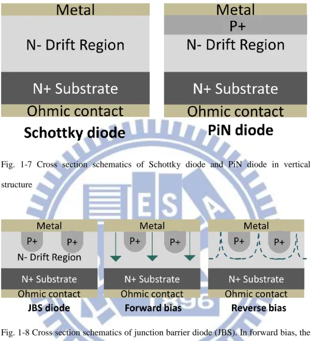
As far as now, SiC-based power devices are the most matured technology among the other wide bandgap materials. 4H-SiC Schottky barrier diodes (SBDs) have been widely used in fast switching and high temperature applications as shown in Fig. 1-7 [27, 28]. The most commonly metals used on 4H-SiC SBDs are nickel (Ni) and titanium (Ti) with Schottky barrier heights (SBH) equal to 1.6 eV and 1.2 eV, respectively. The breakdown of Schottky diode occurs at the interface between metal and SiC.
The PiN diode shown in Fig. 1-8 provides higher breakdown voltage than Schottky barrier diode. With a built-in potential of 2.7 eV, an even lower reverse leakage current in PiN diode is obtained than in Schottky barrier diode, but higher forward voltage drop in PiN diode is not desired in some applications. Although PiN has higher forward voltage drop, Schottky barrier diode has no enough breakdown voltage.
In order to solve this dilemma, junction barrier Schottky (JBS) diode was introduced as a new device. As shown in Fig. 1-8, there are some p-type grids underneath the Schottky contact [29]. In forward operation, the Schottky contact will turn on at low voltage; in reverse bias, the p-type grids will deplete the n-drift region to provide higher breakdown voltage and lower leakage current from Schottky contact. Hence, the JBS diode does not breakdown at the Schottky contact interface, but at the boundary of pn junction.
Different JBS diodes have been proposed to ease the process of p-type dopant activation or to improve the performances of JBS diodes with the same basic theory,
9
like dual-metal trench Schottky diode and MOS trenched Schottky barrier diode [28]. As shown in Fig. 1-9, by etching SiC substrate first, these trenches are filled with high work-function metal or fabricated as trenched MOS capacitor [28]. Both of the devices deplete n-drift region under reverse bias similar to the p-type grids in JBS diode.
The trench junction barrier Schottky barrier (TJBS) diode is shown in Fig.1-10 [30]. TJBS diode is expected to provide more on-current from the sidewall of Schottky contact than JBS, and maintain the same breakdown voltage as JBS. Here, we simulate the TJBS structure in Sentaurus TCAD. We expect to figure out the design guidelines of TJBS.
1-6 Thesis Organization
The first chapter includes the introduction of history of power devices, wide bandgap materials, and fundamentals of SiC crystals. Different structures of SiC-based power devices are introduced briefly. The importance in the quality of epilayers of SiC and different characterization technologies of epilayer-quality are discussed. The next chapter exhibits the theory and setup of DLTS system. Verifications of DLTS system are also resented. Sample preparations of DLTS measurement and results of different treatment are also discussed.
Then, the third chapter contains the simulation of new structures of TJBS and geometric parameters, forward current characteristics, and breakdown voltage compared to JBS. Finally, we will summarize the design guidelines of TJBS. The last chapter is conclusions and suggested future works.
10
Table 1-1 Physical characteristics of Si and main wide bandgap semiconductor [11]. ɛ=ɛr∙ɛ0 , where ɛ0 = 8.85∙10-14 F/cm
Property Si GaAs 6H-SiC 4H-SiC GaN
Diamond Bandgap, Eg (eV) 1.12 1.43 3.03 3.26 3.45 5.45 Dielectric constant ɛr 11.9 13.1 9.66 10.1 9 5.5 Electric Breakdown Field, Ec (MV/cm) 0.3 0.4 2.5 2.2 2 10 Electron Mobility, µn (cm2/V-sec) 1500 8500 // c-axis:80 ┴c-axis:500 1000 1250 2200 Hole Mobility, µp (cm2/V-sec) 600 400 101 115 850 850 Thermal Conductivity, λ (W/cm-K) 1.5 0.46 4.9 4.9 1.3 22 Saturated Electron Drift Velocity (x107 cm/s) 1 1 2 2 2.2 2.7
11
Fig.1-1 In SiC, silicon atom is covalently bonded with 4 carbon atoms in the tetrahedral arrangement [13].
12
13
Fig.1-4 Four Miller Indices (a1 a2 a3 c) in hexagonal structure [14].
Fig.1-5 Comparison of unipolar limit of specific on-resistance versus blocking voltage for some device types in Si and SiC [15].
14
15
Fig. 1-7 Cross section schematics of Schottky diode and PiN diode in vertical structure
Fig. 1-8 Cross section schematics of junction barrier diode (JBS). In forward bias, the Schottky contact will turn on at low voltage; in reverse bias, the p-type grids will deplete n-drift region to provide higher breakdown voltage and smaller leakage [28].
16
Fig. 1-9 Dual-metal trenched Schottky diode (DMTS) with two different metals to achieve and trenched MOS barrier Schottky diode (TMBS) with MOS structure are introduced by the same basic theory of JBS [28].
Fig. 1-10 Device configuration of trenched junction barrier Schottky diode (TJBS) [30]. In forward bias, the Schottky contact will turn on at low voltage,and sidewall of schoottky diode can provide more on-current to lower down its on-resistance; in reverse bias, the p-type grids will deplete n-drift region to maintain breakdown voltage and smaller leakage
17
Chapter 2
Defects in 4H-SiC by deep level transient
spectroscopy
2.1 Introduction to deep level transient spectroscopy (DLTS)
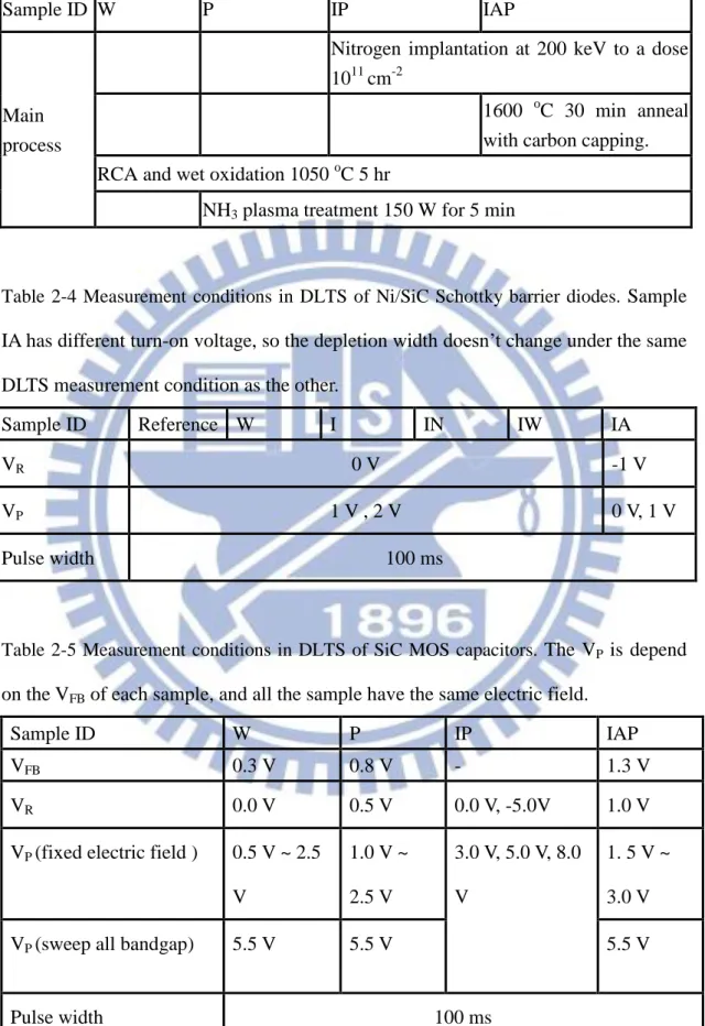
Deep level transient spectroscopy (DLTS) is a defect detection technique, which was first proposed by D. V. Lang in 1974 [31]. DLTS is a capacitance transient spectroscopy and it can acquire more information effectively than traditional defect detection techniques [32].
The concept of DLTS is on the bases of the change in capacitance of depletion region in a pn diode or Schottky diode [31, 33]. The operation principle is shown in Fig. 2-1. First, the diode is kept at a reverse bias VR to empty electrons in depletion
region. Second, the device is pulsed with a voltage VP, so the depletion region
becomes very small. The change in the width of depletion region results in the change in capacitance. The original empty defects capture electrons from conduction band. Last, after pulse, the voltage across the diode returns to the reverse bias VR. The free
majority carrier can responds the bias soon, but the trapped electron cannot. Hence, the depletion region would be wider than its original width to compensate the trapped electrons, which corresponds to a smaller junction capacitance. The trapped electrons will emit from defects eventually, so the depletion region will be back to steady state as well as the junction capacitance [33].
The transient capacitance is a function of time as expressed in eq. (2-1) [33]. According to eq. (2-2), by selecting two different time points t1 and t2, in a transient
18 C(t) = C0[1 − nT 2NDexp(− t τe)], eq. (2-1) δC = C(t1) − C(t2) =2NnT DC0{exp (− t2 τe) − exp(− t1 τe)}, eq. (2-2) where C0 is the capacitance in steady state, 𝑛𝑇 is the defect concentration (cm-3), ND is the donor concentration (cm-3), τe is the emission time of the trapped electron (s),
and t is the time passed (s).
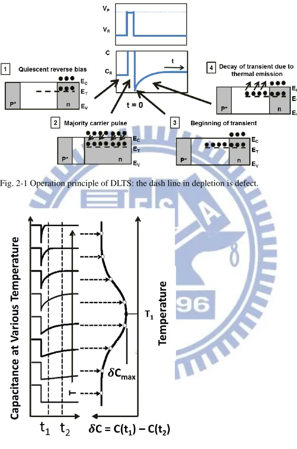
The emission time of trapped electron depends on the depth of the energy level from band edge and the temperature during measurement as shown in eq. (2-3). In Fig. 2-2, if the temperature is low, the change of capacitance will be very slow, so the δC will be very small; at high temperature, the emission time of the trapped electron is short and the change of capacitance will be very fast, so the δC will be very small, too. Consequently, at proper temperature T1, δC will reach its maximum value [33].
By differentiating eq. (2-3) to τe, we can get the relation of τe between t1 and t2 as
expressed by eq. (2-4). With eq. (2-4) and proper temperature T1, we can get the
energy level and the capture cross section of the traps from eq. (2-3). τe = exp((EγC−ET)/kT)
nσnT2 ,
eq. (2-3) τe,max =ln(tt2−t1
2⁄ )t1 , eq. (2-4) where τe is the emission time of trapped electron (s), EC is the conduction band energy
(eV), ET is the energy of the deep trap in bandgap (eV), k is the Boltzmann constant, T
is the temperature in Kelvin, 𝛾𝑛 is a constant (cm-2·s-1·T-2), and σn is the capture cross section (cm2).
As mentioned above, we can acquire the deep trap level and capture cross section from the DLTS effectively [31]. Since the introduction of DLTS in 1974, many improvements have been proposed, like lock-in amplifier DLTS, CCDLTS, Correction DLTS, isothermal DLTS, and Laplace DLTS [33]. Here, we established a conventional
19 DLTS system.
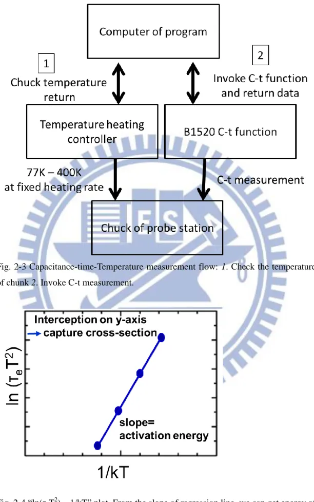
2.2 Setup of DLTS system
In order to detect the defects in the 4H-SiC epi-layer and the traps after ion implantation and dopant activation processes, we establish a conventional DLTS system. The DLTS system requires two basic elements: transient capacitance meter (C-t meter) and temperature controller [31].
The C-t meter in our DLTS system is a multi-frequency capacitance measurement unit of module B1520A appended in the Agilent B1500A semiconductor device parameter analyzer. The specifications of the C-t function of the B1520A are listed in Table 2-1 [34]. Measurements are conducted in a probe station of model Lake Shore CPX-VF with a temperature controller. The probe station can be vacuumed to about 10-5 torr to avoid the condensation of moisture and residual gases. The temperature of chuck can be cooled down to 77 K by liquid N2 circulation and be
raised with regular ramping rate to 400 K by temperature heating controller.
Computer program written in HT BAISC language controls the B1520A and the temperature controller simultaneously [35, 36]. The algorism of the program is presented in Fig. 2-3. First, the chuck is cooled down to 77 K and maintaining at 77 K for 20 minutes with probing on device. After setting measurement conditions in program, the measurement procedure starts. During the Capacitance-time-temperature (C-t-T) measurement, the program will acquire the temperature of chuck firstly. Then, the program will invoke the B1520A to execute a C-t measurement and return the data to computer. By repeat these two steps, the C-t-T measurement are done till the temperature of chuck researches 400 K. By changing t1 and t2 according to eq. (2-4),
20
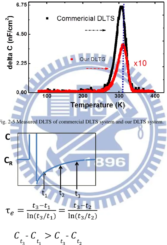
Fig. 2-4. Then, we can draw the “ln(τeT2) – 1/kT” plot [33]. From the slope of the
linear regression line, we can obtain the energy of the traps, and from the interception on y-axis, we can obtain the capture cross section [33].
2.3 Verifications of DLTS system
To verify our DLTS system, the same sample was measured by our DLTS system and by a commercial purchased DLTS system. The commercial DLTS system is provided by the Sula Technologies Co. and was installed in Professor J. F. Chen’s lab in the Department of Electrophysics of National Chiao Tung University. The sample used here is sample IA. The process flow will be introduced in next section. Only substrate defect is observed on sample IA from the DLTS result.
Fig. 2-5 shows the DLTS results measured by the commercial DLTS system and our system. For the same emission time constant, the signal peak occurs at the same temperature. The large signal intensity difference comes from the relatively slow sampling rate of the B1520A. As shown in Fig. 2-6, the selection in different time points will have the same time emission constant but different δC. The shortest sampling rate of the commercial DLTS system is less than 100 s [37]. This system selects time points automatically according to the specified emission time constant, but the actually time points are unknown. For our DLTS system, the actually time points is known. However, the relatively slow sampling rate of the B1520A, 10ms, is the main reason for the large difference in signal intensity. The signal intensity doesn’t affect the temperature position of peak, so the function of our DLTS system is verified.
21
2.4 Sample fabrication for DLTS measurements
2.4.1 Ni/SiC Schottky barrier diode
The starting material is a 4-inch (0 0 0 -1)-oriented n-type 4H-SiC substrate with a 5-m-thick epi-layer purchased from Cree. The substrate is doped by nitrogen to a concentration of 5x1018 cm-3. The nitrogen concentration ND in the epi-layer is equal
to 1015 cm-3. The 4H-SiC wafer was cut into small pieces. These samples were cleaned by standard RCA clean process and followed by different treatments as summarized in Table 2-2. These are four kinds of treatments. They are wet oxidation (W), nitrogen ion implantation (I), N2 annealing (N), and 1600oC high temperature
activation (A). The sample ID indicates the composition of these treatments. For example, sample IN indicates that the sample receives nitrogen ion implantation and N2 annealing. The samples experienced 1600 oC annealing were capped with carbon
layer before annealing to avoid Si sublimation. The carbon layer was removed by a 900 oC oxidation for 1 hour in O2 ambient. Before depositing PECVD oxide as field
oxide, all the substrates were cleaned by SPM (H2SO4:H2O2 = 3:1) and dipped by
diluted HF. A 100-nm-thick Ni and a 10-nm-thick TiN were sputtered at samples’ backside followed by a 1000oC RTA for 30s to form backside ohmic contact. Then, contact holes were defined by conventional lithography process and the field oxide was etched by BOE. The Schottky metal of 10-nm-thick Ni was deposited by a sputtering system. Samples were immediately loaded into a thermal coater within 5 min to evaporate a 300-nm-thick Al as electrode. Finally, the residual metal was removed by a lift-off process. The schematic structure of the Ni/SiC Schottky barrier diode (SBD) is shown in Fig. 2-7.
22
2.4.1 SiC MOS capacitor
Metal-oxide-semiconductor (MOS) capacitors were fabricated on the same 4H-SiC epi-wafer. After standard RCA clean, some samples were implanted by nitrogen at 200 keV to a dose of 1011 cm-2. After ion implantation, samples were cleaned by RCA clean process again and followed by 1050 oC wet oxidation for 5 hr. Some samples received NH3 plasma treatment for 5 min to reduce the interface states
(Dit) [38]. The main process conditions for the MOS capacitors are summarized in
Table 2-3. There are for process steps: wet oxidation (W), nitrogen ion implantation (I), NH3 plasma treatment (P), and high temperature activation (A). Aluminum was
deposited by thermal evaporation and patterned by lithography and wet etching to form gate electrode. The backside of wafer was cleaned by BOE and followed by Al deposition as backside contact. All the samples were sintered at 400 oC for 30 min in N2 ambient. The schematic structure of the SiC MOS capacitor is shown in Fig. 2-8.
2.5 Ni/SiC Schottky barrier diode
2.5.1 Current - voltage characteristics
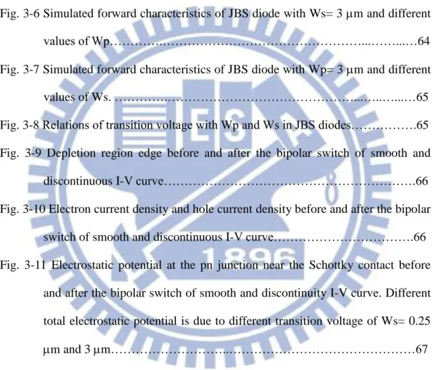
The I-V characteristics of the Ni/4H-SiC Schottky barrier diode (SBD) fabricated with different processes as listed in Table 2-2 are shown in Fig. 2-9. The reference sample shows ideal SBD characteristics. The Schottky barrier height is 1.5 eV and the ideality factor is 1.12. For the ion implanted samples, I, IN, and IW, the distorted I-V curves and low forward current at 3 V are observed at forward bias. If we raising the measurement temperature, kink phenomenon occurs and the forward current increases to normal value at high forward bias as shown in Fig. 2-10 ~ Fig. 2-12. This observation can be explained by a two energy barriers model - one is the Schottky barrier and the other one comes from the damaged region formed by ion implantation.
23
The raising of forward bias bends the energy band gradually so that electrons can overcome the two barriers sequentially. The kink indicates electron overcomes the potential barrier due to the high-low junction. As the measurement temperature becomes higher, electron can overcome the barrier easier by thermionic emission. Hence, the kink phenomenon fades out and the cut-in voltage drops due to higher temperature. The other phenomenon like higher resistance is electrons suffers from more phonon scattering at higher temperature [39].
Sample IA has the same forward current at 3 V as the reference sample, but kink phenomenon is observed at lower voltage. Because the reverse current increases apparently, it is suspected that there are two Schottky barrier heights at the Ni/SiC contact. From thermionic emission equation [39], the two extracted Schottky barrier heights are 0.6 eV and 1.3 eV. The low Schottky barrier may be originated from the surface local defects induced by ion implantation and activation [40]. Fig. 2-13 and Fig. 2-14 shows the cross sectional TEM micrographs of sample I and sample IA, and much poorer surface morphology is observed on sample IA which is corresponding to the double barrier. The high Schottky barrier height is lower than the Schottky barrier of the reference sample. During the epi-layer growth of SiC, the gas flow ratio of C/Si has direct impact on the Schottky barrier height [41]. The lower the C/Si ratio is, the lower the Shcottky barrier height is. This implies more carbon vacancy in SiC under the lower C/Si ratio condition. Because of the generation of carbon vacancy after high temperature, a relatively lower Schottky barrier is measured in sample IA compared to the reference sample [42].
24
2.5.2 Capacitance - voltage characteristics
The C-V characteristics of all samples are shown in Fig. 2-15. The reference sample shows the largest junction capacitance, but for samples I, IN, and IW, relatively low capacitance was measured. Because of the ion implantation damage, the damaged region is easily depleted so the total junction capacitance is much lower than the reference sample. As for sample IA, the 1600 oC annealing activates the nitrogen from ion implantation, so the effective ND at the surface region may be slightly higher
than original ND as observed in Fig.2-16. Theoretically, the capacitance should be
larger due to the higher ND, but the result is opposite. The relatively low Schottky
barrier height and surface defects may be the reason for the lower capacitance compared to the reference sample.
2.5.3 DLTS results of Ni/SiC Schottky barrier diode
The DLTS measurement conditions are listed in Table 2-4. Sample IA has different measurement condition because of the smaller turn-on voltage due to its relatively low Schottky barrier height. This measurement condition can reflect the change in depletion width clearly.
The DLTS of reference sample is shown in Fig. 2-17. There is no significant signal compared to the DLTS of sample I shown in Fig. 2-18. The DLTS of sample I has distinct signals at 270 K and 370 K obviously. These signals are too broad to result from a single trap. It’s impossible to identify the trap energy because the severe overlap of signals. Different pulse voltages (VP) of sample I have similar results. The
slightly difference in signal intensity comes from the difference in depletion width at different VP, so different amounts of traps can be detected. Besides, if the VP becomes
25
higher, the edge of the depletion region becomes closer to the surface of substrate. The spatial distribution of defect can be detected.
In order to eliminate the ion implantation induced defects in the 4H-SiC epi-layer, post implantation annealing was conducted. Annealing at 1050 oC for 5 hour in N2 or
O2 ambient was performed for defect recovery. Some defects can be annihilated by
thermal annealing and oxidation [43]. In order to avoid defects generation during oxidation, DLTS of sample W was also measured and the result is shown in Fig. 2-19. No significant signal is observed. As the results in Fig 2-20 and Fig 2-21, the DLTS of sample IN and sample IW still have obvious signals. Even they are distinct to be identified, but all of them are still too broad to be considered as a single trap. For VP =
1 V, both of the samples IN and IW have almost identical spectra, which represents the same defects. While VP = 2 V, a new signal appears at 170 K, which is located
spatially near the SiC surface. We can distinguish it barely composed of two traps ID4
and ID8 with activation energies EC-0.37 eV and EC-0.45 eV, respectively [44]. As to
the extra peak at 300 K in the DLTS of sample IW, it’s a single trap S2 with activation energy EC-0.70 eV [45]. In the DLTS of sample IN and sample IW, the other
un-discussed signals are still too broad to be a single trap, and are hard to be distinguished.
The DLTS result of sample IA is shown in Fig 2-22, almost all traps are vanished, and only one trap, known as Z1/2 with activation energy EC-0.60eV, is observed [44].
High temperature annealing is effective in reducing defects, but in the meanwhile it could generate large amount of Z1/2 trap [42]. By drawing the ln(τeT2) – 1/kT plot,
activation energy and capture cross section can be extracted from the slope and interception on y-axis, respectively. The extracted results are shown in Fig. 2-23.
On sample I, traps ID4 and ID8 are not obvious, but after 1050 oC annealing they
26
together to form stable structural defects. Oxidation of SiC will form carbon interstitial (Ci) [46]. Some Ci will pile up at the interface between SiO2 and SiC,
which leads to large amount of Dit, and some Ci will diffuse into the substrate [46, 47].
From previous study, the trap S2 is a complex of Ci, so the appearance of trap S2 in
sample IW near SiC surface is reasonable [45]. After 1600 oC annealing, the trap Z1/2
shows up, which corresponds to carbon vacancy (Vc) [42]. The origin of Z1/2 in the
epi-layer may diffuse from the n+ SiC substrate where high concentration of VC
presents [42]. The Z1/2 traps can be reduced by thermal oxidation or carbon
implantation to improve the quality of epi-layers [42, 46].
2.6 SiC MOS capacitor
2.6.1 Capacitance – voltage characteristics
The high frequency and quasi-static C-V curves of SiC MOS capacitors are shown from Fig. 2-24 to Fig. 2-27. Expect for the sample IP, the Dit extracted by the
high-low frequency method are shown in Fig. 2-28 [38]. It can be observed that the samples with NH3 plasma treatment have lower Dit than the sample without plasma
treatment [38]. As to the sample IP, ion implantation produces an damaged region as mentioned before. According to previous study, the MOS capacitor fabricated on high resistive substrate suffers from seriously series resistance [48]. As shown in Fig. 2-29, the equivalent circuit has to be modified to accommodate the frequency dependence. With the presence of highly resistive substrate, the measured accumulation capacitance at high frequency is relatively small to the capacitance of oxide, whereas the accumulation capacitance at low frequency is not affected [48]. Fig.2-30 shows the simulated and measured C-V curves from previous study which matches our observation on sample I [48].
27
For C-V characteristics over temperatures, since sample IP exhibits abnormal C-V characteristic, it is not discussed here. A large flat band voltage shift can be observed on the rest samples as shown from Figs. 2-31, 3-32, and 3-33, flat band voltage shift is originated from the large amount of Dit [47]. At high temperature, the
traps are capable of emitting the trapped electrons by thermal emission, and the response is fast enough to follow the gate voltage sweep. At low temperature, the same traps are unable to thermally emit their captured electrons within the time frame of the measurement, so that the trapped charge is frozen in. These trapped electrons at Dit in all the samples make the flat band voltage shift.
2.6.2 DLTS results of SiC MOS capacitor
The DLTS measurements are performed on the SiC MOS capacitors. There are three types of traps can be identified by DLTS as shown in Fig. 2-34. They are substrate defect, interface state (Dit), and oxide trap [49]. It’s relatively easy to
distinguish substrate defect from the other trap, because substrate defect does not distribute continuously in the bandgap. The Dit and oxide trap are continuously
distributed in the bandgap so that both of them result in broader DLTS signals. Oxide trap has relatively slow emission time constant and the time constant depends on electric field in the gate dielectric [49]. The signal intensity of substrate defect and Dit
will saturate as the VP increasing due to the limited defect density of them near
surface. For oxide trap, the signal intensity keeps increasing, because more electrons are trapped deeper into the dielectric [54]. Dipole-like relaxation will result in opposite transient capacitance as shown in Fig. 2-35 [50]. The dipoles will be arranged during the pulse, and become disordered during the measurement, so the transient capacitance will decrease gradually.
28
SiC MOS capacitors with different processes listed in Table 2-3 were fabricated. Because of different flat band voltages on different samples, the parameters of DLTS measurement are varied for different samples as listed in Table 2-5. The Vp was
adjusted so that the electric field in dielectrics are the same. Because of the flat band voltage shift at low temperature, the larger VP was applied to make sure all the Dit will
be measured.
In Fig. 2-36, the DLTS of sample W exhibits a continuous signal. The intensity of signal increases and the peak position changes as VP increasing. Only oxide trap
exhibits the behavior with the dependence with applied voltage. For VP = 5.5 V, the
dipole-like relaxation becomes obvious. Because at high temperature the de-trapping of electron becomes very fast, the transient capacitance due to electron de-trapping is too fast to be measured, so the relatively slow dipole-like relaxation becomes the dominant phenomenon. At higher VP, it will induce more dipoles, so the dipole-like
relaxation becomes more obvious. If applying eq. (2-5) to transform the DLTS result to the corresponding Dit, the Dit extracted from DLTS is much higher than that
extracted from the high-low frequency method as shown in Fig. 2-37 [26]. Because of the presence of oxide trap, the Dit extracted from DLTS includes oxide trap and Dit,
and we cannot separate them apart from the DLTS signal. The DLTS of sample P as shown in Fig.2-38 shows similar VP dependence as that on sample W, and oxide trap
signal dominates the entire DLTS. The Dit extracted from DLTS is also higher than
that extracted from the high-low frequency method as shown in Fig.2-39. E t = EC− 𝑘𝑇𝑙𝑛 {γnσnT2(t2−t1)
𝑙𝑛(t2/t1) } , D t = −
ɛ𝑟ɛ0NDCOX
𝑘𝑇 𝑡13ln(t2/t1),
eq. (2-5) [26] where Eit is the energy level below conduction band (eV), ɛ𝑟 is the dielectric
constant of SiC, ɛ0 is the vacuum permittivity (F/cm), Ct1 is the transient
29
Sample IP has a high resistance damaged layer due to ion implantation induced damages. In Fig. 2-40, the DLTS of sample IP shows three peaks as the VP increases
from 3 V to 8 V. More electrons are trapped, so the signal becomes more obvious. The DLTS theory is based on the change in depletion width [31]. It should be noted that only the traps above Fermi level can be detected, because the trapped electrons are hard to be emitted [52]. If we change the VR, the DLTS signal becomes weak, because
the depletion region is not dominated by the damaged region. Instead, the un-damaged epi-layer dominates the most of depletion, so the δC will be very small. Hence, we redraw it in Fig. 2-41, and a peak is observed at 370 K compared to VR = 0 V. The
DLTS of the MOS capacitor sample IP and the SBD sample IW exhibit the same signal at the same temperature position which matches to each other very well.
Sample IAP was annealed at 1600 oC to repair the lattice damages and to activate dopants. In Fig. 2-42 the DLTS of sample IAP is the same as that of sample W, except the peak related to substrate defect at 270 K. The substrate defect is detected on SBD sample IA, too. In Fig. 2-43, the Dit extracted by DLTS measurement is higher than
that extracted by high-low frequency method. Besides, the Dit extracted by DLTS
measurement is affected by substrate defect.
2.7 Summary of DLTS results
Different ion implantation damages in 4H-SiC epi-layer have been investigated by DLTS. These traps are corresponding to ID4 and ID8 with activation energies
EC-0.37 eV and EC-0.45 eV, respectively. Due to severe overlap of signals, the other
defects are hard to be distinguished [44]. The carbon interstitial generated from thermal oxidation induced a new trap S2 with activation energy EC-0.70 eV [45, 46].
30
surface of substrate. The DLTS of the SBD sample IW is consistent with that of the MOS capacitor sample IP. For the 1600 oC annealed sample, both diode and capacitor have the defect Z1/2 with activation energy EC-0.60 eV, which is generated after higher
temperature annealing [42, 44].
Oxide traps dominates the DLTS result of the MOS capacitor [49]. With the presence of oxide trap, substrate defect, and dipole-like relaxation, eq. (2-5) would result in overestimation of Dit in comparison with the Dit extracted from high-low

![Table 1-1 Physical characteristics of Si and main wide bandgap semiconductor [11]](https://thumb-ap.123doks.com/thumbv2/9libinfo/8122399.165946/27.892.130.766.166.888/table-physical-characteristics-si-main-wide-bandgap-semiconductor.webp)
![Fig. 1-9 Dual-metal trenched Schottky diode (DMTS) with two different metals to achieve and trenched MOS barrier Schottky diode (TMBS) with MOS structure are introduced by the same basic theory of JBS [28]](https://thumb-ap.123doks.com/thumbv2/9libinfo/8122399.165946/33.892.133.807.124.867/trenched-schottky-different-achieve-trenched-schottky-structure-introduced.webp)