國立交通大學
電子物理學系暨研究所
碩士學位論文
以分子束磊晶法成長氧化錳鋅
稀磁性半導體的磁學與光學特性
Magnetic and optical properties of ZnMnO
diluted magnetic semiconductor grown by
molecular beam epitaxy
研究生 : 陳宣劭
指導教授 : 周武清 博士
以分子束磊晶法成長氧化錳鋅稀磁性半導體的磁學與光學特性 Magnetic and optical properties of ZnMnO diluted magnetic
semiconductor grown by molecular beam epitaxy
研究生:陳宣劭 指導教授:周武清 博士
Student: Hsien-Shao Chen Advisor: Dr. Wu-Ching Chou
國 立 交 通 大 學 電子物理學系暨研究所
碩 士 論 文
A Thesis
Submitted to Department of Electrophysics College of Science
National Chiao Tung University in partial Fulfillment of the Requirements
for the Degree of Master in
Electrophysics
June 2013
Hsinchu, Taiwan, Republic of China
以分子束磊晶法成長氧化錳鋅
稀磁性半導體的磁學與光學特性
研究生:陳宣劭 指導教授:周武清 博士 國立交通大學 電子物理學系暨研究所 碩士班摘要
本研究利用分子束磊晶方法將高品質的氧化錳鋅薄膜成長於以 氮化鋁作為緩衝層的矽(111)基板上,並藉由光激螢光系統及超導量 子干涉儀等方法量測成長出的氧化錳鋅薄膜在不同錳濃度下的光學 與磁學特性並進行分析。 從光激螢光光譜中可以確認氧化鋅薄膜具有良好的發光特性,並 且能觀察到激子復合發光會隨著錳濃度上升而急遽減弱,同時也因此 可在較高錳濃度的樣品中觀察到共振拉曼現象,並可以瀑布模型解釋 不同訊號峰值的強度變化。 而從室溫磁滯曲線中可發現不同濃度下的氧化錳鋅樣品皆具有 室溫鐵磁性,其中也包括了未進行錳摻雜的純氧化鋅樣品,對此我們 採用束縛磁極化子模型來描述不同樣品中的磁性行為,並推測氧化鋅 樣品中的鐵磁性可能由缺陷誘發。Magnetic and optical properties of ZnMnO diluted
magnetic semiconductor grown by molecular beam
epitaxy
Student: Hsien-Shao Chen Advisor: Dr. Wu-Ching Chou
Department of Electrophysics National Chiao Tung University
Abstract
This research is dedicated to the growth of high quality ZnMnO thin films on Si(111) substrates with AlN as buffer layer by molecular beam epitaxy (MBE). The optical and magnetic properties were investigated by photoluminescence (PL) system and superconducting quantum interference device (SQUID).
The PL spectra confirmed good emission property in ZnO sample, and the quench of excitonic transitions as Mn doping concentration increased was observed. Hence the resonant Raman scattering phenomenon became clear in samples with higher Mn doping concentration and the intensity variation of different peaks could be explained by cascade model.
Room temperature magnetic hysteresis loops indicated the existence of room temperature ferromagnetism in all ZnMnO samples including ZnO. Bound magnetic polaron model is employed to describe the distinct
magnetic properties in ZnMnO samples and the ferromagnetism in ZnO could be inferred that is induced by defects.
Acknowledgement
誌謝
碩士的兩年時光倏忽即逝,不知不覺間我也到了離開校園即將踏 入社會的年齡。我之所以能夠順利畢業最先要感謝的便是我的指導老 師 周武清博士,老師提供給我們相當良好的研究環境讓我們能夠安 心順利地進行研究,在我們遭遇困難時以專業的學識教導我們,同時 也用深厚的學術素養為我們指引方向。 還有時常關心我、給予我指導的李寧學長、彥丞學長、文忠學長、 崑峯學長和安傑學長,特別是安傑學長常在我不知所措時指點我,真 的是不勝感激。也感謝助理小育姐姐幫我們處理實驗室的行政事務, 讓我們無須為其他事情分心而可以專心致力於實驗。 謝謝在碩一剛進實驗室時教導我儀器操作,讓我能較快熟悉實驗 室環境的偉仕學長、蓉菲學姐、維綸學長、祐霖學長、靜宜學姐。 還有同屆的其他三位同學,嘉華、明睿、湘穎,以及四位學弟妹 阿丹、阿毛、乖乖、戴戴,謝謝你們常常幫我買便當還會包容我的冷 笑話,而且還會幫我慶祝生日、一起去唱歌,不過如果湘穎可以不要 常常生氣那就更好了。 最後還要謝謝我的家人,我的父親、母親、哥哥、姐姐、姐夫, 因為有你們在背後的支持才讓我能夠無後顧之憂的完成學業。Contents
Abstract (Chinese)...I Abstract (English)...II Acknowledgement...IV Contents...V Table Captions...VII Figure Captions...VIII Chapter.1 Introduction...1 1.1 Motivation...1 1.2 Paper review...2Chapter.2 Experimental details...7
2.1 Molecular beam epitaxy (MBE)...7
2.2 Sample Preparation...8
2.3 Photoluminescence (PL)...9
2.4 Scanning electron microscope (SEM)...9
2.5 X-ray absorption spectroscopy (XAS)...10
2.6 Superconducting quantum interference device (SQUID)...10
Chapter.3 Result & Discussions...17
3.1 Surface morphology analyze...17
3.2 Photoluminescence spectra of ZnO and ZnMnO...20
3.4 Magnetic behavior in ZnMnO...33
Chapter.4 Conclusion...47
Table Captions
Table.2-1 Mn doping concentration of ZnMnO samples...13 Table.3-1 The phonon replica peak positions of Zn0.931Mn0.069O...27
Table.3-2 The energy difference between nth mode and (n-1)th mode...28
Figure Captions
Fig.1-1 (a) Electrical spin injection in an epitaxial GaMnAs ferromagnetic semiconductor heterostructure; (b) EL intensity (black curve) at 6 K and 1000 Oe with its corresponding polarization (red
curve)...5
Fig.1-2 The comparison of Curie temperature with various DMS materials...6
Fig.2-1 Plasma assisted molecular beam epitaxy system...12
Fig.2-2 The schematic of photoluminescence measurement...14
Fig.2-3 Scanning electron microscopy system...15
Fig.2-4 Schematic of superconducting quantum interference device...16
Fig.3-1 SEM top-view images of Zn1-xMnxO samples, (a) x = 0; (b) x = 0.003; (c) x = 0.0054; (d) x = 0.0159; (e) x = 0.0373 and (f) x = 0.0693...18
Fig.3-2 The SEM cross-section images of Zn1-xMnxO samples, (a) x = 0; (b) x = 0.003; (c) x = 0.0054; (d) x = 0.0159; (e) x = 0.0373 and (f) x = 0.0693...19
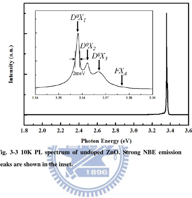
Fig.3-3 The 10K PL spectrum of undoped ZnO. Strong NBE emission peaks are shown in the inset...22
Fig.3-4 (a) The temperature dependent PL spectra of undoped ZnO; (b) the temperature dependent peak positions plot. The Varshni fitting results were shown in solid lines...23
Fig.3-5 Low temperature PL spectra of Zn1-xMnxO samples, where x = 0 ~ 6.97...24
Fig.3-6 RRS spectrum of Zn0.931Mn0.069O. The phonon replica peaks up to
11 LO were clearly observed...25 Fig.3-7 Schematics of RRS and relaxation path...26 Fig.3-8 The Mn2+L-edge energy transitions diagram...31
Fig.3-9 L-edge spectra of Zn1-xMnxO samples, where x = 0.003 ~ 0.069.
Their L2 and L3 peaks positions matched the peaks of Mn
2+
ion in MnO. The observed transitions energies of E1, E2, E3, E4 and E5 are 640.59 eV, 641.96 eV, 644.12 eV, 650.89 eV and 652.66 eV, respectively...32 Fig.3-10 Temperature dependent magnetic hysteresis loops of Zn0.979Mn0.021O...37
Fig.3-11 Temperature dependent remanant magnetization of Zn0.979Mn0.021O. The spontaneous magnetization fitting is shown by red
line...38 Fig.3-12 Temperature dependent magnetization curves of Zn0.979Mn0.021O.
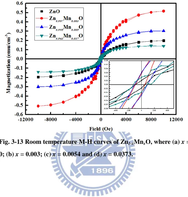
The ZFC and FC curves were shown in black line and red line, respectively...39 Fig.3-13 Room temperature M-H curves of Zn1-xMnxO, where (a) x = 0;
(b) x = 0.003; (c) x = 0.0054 and (d) x = 0.0373...40 Fig.3-14 The relationship between remanent magnetization (red line), coervice field (black line) and Mn doping concentration plot...41 Fig.3-15 Zero field cooling temperature dependent magnetization curves of Zn0.979Mn0.021O. The Bloch spin wave function fitting was shown in the
red line...42 Fig.3-16 The relationship between the effective exchange constant (Jex)
and Mn doping concentration...43 Fig.3-17 Effective Bohr magneton contributed from ferromagnetic Mn
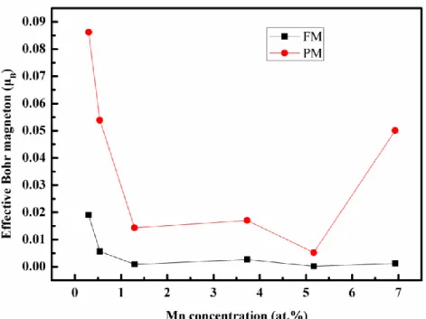
ions (black points) and paramagnetic Mn ions (red points)...44 Fig.3-18 The relative ratio of FM to PM Mn ions in different Mn doping concentration samples...45 Fig.3-19 Schematics of mixed magnetic phases in Zn1-xMnxO samples..46
Chapter 1 Introduction
1.1 Motivation
Accompanied with technology development of semiconductor materials and devices, integrated circuit (IC) devices have been developed to high integration, fast signal process and excellent reliability. Operation of ICs uses external electric field to manipulate the flow of carriers in semiconductors by controlling the charge properties of free carriers. By switching the current to high or low to control the logic gates results in high energy consumption and leads to high operating temperature. Conventional electronic device operation base on the control of current density and electrical field limits the switching frequency and increases energy cost. Spintronics devices provide solution to these problems. The operation of spintronic devices bases on the control of spin polarization and spin coupling of charge carriers. It consumes less power and high-speed switching is possible [1-2].
Despite the great advantage of spintronic devices, detailed physical properties of spintronics devices are yet to be discovered. Research groups have demonstrated the operation of spintronic devices based on diluted magnetic semiconductor (DMS) materials, as shown in Fig. 1-1 is an example of spin light emitting diode. But these devices could only operate at low temperature [3-5]. Therefore, it is urgent to develop novel DMS materials which could be used to fabricate spintronic devices working at room temperature.
1.2 Paper review
The most important issue for the development of spintronics devices is to study magneto-photonic properties, which combine the magnetism and photonic properties of spintronics materials [6]. Earlier researches focused on the injection of spin electrons from ferromagnetic metals to semiconductors and devoted to the epitaxial growth of transition metals (ex: iron, cobalt, nickel, and etc.) on semiconductor substrates [2]. Due to the crystal structure mismatch and band alignment difference between the transition metals and semiconductors, the efficiency of spin injection is strictly limited to less than 1% [7-8].
The concern of high spin injection efficiency has shifted the focus from transition metal/semiconductor system to half-metal material. The half-filled spin polarization state providing near 100% spin polarization [9]. In addition, many of half-metal materials exhibit very large Curie temperatures exceeding room temperature. However, second phase and interlayer between half-metal material and semiconductor could be easily formed due to the crystal structure difference. Thus, half-metal material still suffered from the large contact resistance at the hetero-junction [10]. Transition metal lightly doped into semiconductor, which is also known as diluted magnetic semiconductor (DMS) material [11-12], has a similar crystal structure to the host semiconductor. As a result, good crystal quality and high efficiency of spin injection from DMS to semiconductor could be achieved. At the temperature below the Curie temperature, the Zeeman splitting of conducting carriers could induce spin polarization [13] for the application of spintronic devices.
However, the Curie temperatures of most DMS materials are far lower than room temperature. For the fabrication of spintronic devices based on DMS, the Curie temperature must be higher than the ambient temperature. In 2000, T. Dietl et al. [14] theoretically calculated the Curie temperature of Mn-doped GaN and ZnO, as shown in Fig.1-2. They predicted that the Curie temperature could be higher than 300 K.
ZnO is a direct band gap semiconductor with emission photon energy around 3.37 eV at 10K [15-17]. The exciton binding energy of ZnO is 60 meV, providing exciton emission at room temperature. Besides, zinc and oxygen are sufficient supply in nature. ZnMnO is one member of the ZnO based DMS material. Manganese doping in ZnO provides divalent manganese, which could have a half filled d orbital. The parallel spin direction results in the quantum numbers s = 5/2, l = 0. Therefore, the Mn2+ ions could contribute more magnetic spin moment than other valence states.
Some references reported that ZnMnO could present magnetic hysteresis loop at room temperature, implied the room temperature ferromagnetism (RTFM) [18-19]. However, other research groups observed para-magnetism or antiferro-magnetism in ZnMnO at room temperature [20-21]. Furthermore, ferromagnetic properties have also been investigated in pure ZnO thin film without doping transition metals [22-24], revealing complicate magnetic properties of ZnO and ZnMnO.
In this work, ZnMnO DMS were grown by plasma-assisted molecular beam epitaxy. Structural, optical and magnetic properties of ZnMnO were studied. In Chapter 2, experimental details will be
described. Results and discussions will be presented in Chapter 3. Finally, a summary is given in Chapter 4.
Fig.1-1 (a) Electrical spin injection in an epitaxial GaMnAs ferromagnetic semiconductor heterostructure; (b) EL intensity (black curve) at 6 K and 1000 Oe with its corresponding polarization (red curve). [5]
Fig.1-2 The comparison of Curie temperature with various DMS materials [14].
Chapter 2 Experimental details
In this chapter, we describe the plasma-assisted molecular beam epitaxy (PA-MBE) system and other measurements which were employed to characterize the samples, including scanning electron microscope (SEM), photoluminescence (PL) and superconducting quantum interference device (SQUID).
2.1 Molecular beam epitaxy (MBE)
Molecular beam epitaxy is a superior method to grow materials with high crystal quality. The growth rate of MBE can be controlled as slower as 1 Å /s. MBE system requires ultra-high vacuum, up to 10-11 Torr, leading molecular beams with high mean free paths onto substrate directly with low collision possibility to achieve very high crystal quality. Various structures like thin film, nanocrystals, quantum dots and quantum wells could be grown by MBE system under different growth condition. Within growth process, solid source elements are heated in isolated crucibles until they begin to sublime slowly. Meanwhile, the cell flux and hence growth rate can be manipulated by change cell temperatures.
During the growth process, in-situ reflection high-energy electron diffraction (RHEED) can be used for monitoring the growth status. RHEED could provide information about surface morphology by showing spotty or streaky patterns on the phosphor screen.
The present MBE system is made by SVTA from the U.S.A., as shown in Fig. 2-1, with ultra high vacuum growth chamber and load lock
chamber. Six solid elements are zinc (Zn), magnesium (Mg), cadmium (Cd), tellurium (Te), selenium (Se), manganese (Mn). Two plasma sources are oxygen (O2) and nitrogen (N2), which are activated by RF power. The substrates were mounted to a 2” manipulator with a heater which can heat up to 900°C and the manipulator is able to rotate with constant angular velocity for uniform growth. The flux gauge could detect the beam equivalent pressure (BEP) of each cell, providing useful information to adjust the content of our samples.
2.2 Sample Preparation
In this study, ZnO and Zn1-xMnxO samples were grown on silicon
(111) substrates with AlN buffer layers. AlN thin films grown on Si(111) were provided by Professor Kao, department of electronic engineering, Chung-Yuan Christian University. The surface roughness of AlN thin films is only 0.6 nm and the lattice mismatch between AlN and ZnO is only 4.4%. Therefore, AlN is a good choice as a buffer layer for ZnO.
The substrates were cleaned by HCl:H20=1:20 solutions with supersonic rinse for 15 minutes and then cleaned in de-ionized water. The substrates were then mounted on a moly block by using indium glues then transfer to growth chamber via load lock chamber.
Afterward, samples were transferred into growth chamber and heated to 850°C for desorption and surface reconstruction until the appearance of the RHEED patterns. Then the substrate temperature was decreased to 660°C for growth. In this study, the Zn cell temperature was set at 280°C. The oxygen flow rate was 0.6 SCCM with RF power 250 W. The Mn cell
temperatures were varied from 680°C to 770°C, to control Mn doping concentration. The Mn doping concentration was measured by energy dispersion X-ray spectroscopy (EDX). The Mn concentration of ZnMnO samples are listed in Table.2-1.
2.3 Photoluminescence (PL)
The He-Cd continuous wave mode laser with wavelength 325 nm (3.815 eV) line is used as an excitation light source and the laser beam is focused and redirected by lens to incident on the samples. The samples were mounted on the copper holder in the vacuum chamber and could be cooled by closed-cycle refrigerator. A heater is set to adjust the measurement temperature from 10K to 300K.
The photoluminescence signal is analyzed by a Horiba-Jobin Yvon
iHR550 (2400 grooves/mm grating) spectrometer with a liquid nitrogen
cooled CCD detector, the energy resolution of PL spectrometer is about 0.3 meV. The experimental set-up of PL is shown in Fig.2-2.
2.4 Scanning electron microscope (SEM)
Scanning electron microscope (SEM), as shown in Fig. 2-3, is one kind of electron microscope that produces images by focused scanning electron beam. The incident electrons scatter with surface atoms of the sample, producing various signals, including secondary electrons (SE), back-scattered electrons (BSE), characteristic X-rays (EDX), infra-red to ultra-violet light (cathodoluminescence, CL). Secondary electron imaging
is the standard SEM image mode which could achieve resolution at about 1.5 nm at acceleration voltage of 15 kV.
2.5 X-ray absorption spectroscopy (XAS)
X-ray absorption spectroscopy (XAS) is used for the determination of the local geometry and electronic structure of materials. Synchrotron radiation is usually used as X-ray excitation source since its tunability of photon energy which could varied from 100 to 100,000 eV. In this experiment, the measurement system was set in National Synchrotron Radiation Research Center (NSRRC, Hsinchu, Taiwan) at beam line BL-17B1.
The extremely short wavelength synchrotron radiation excites core electrons to measure their energy level transitions. XAS could be used for determination of valence states, coordination environment and subtle geometrical distortions of matters.
2.6 Superconducting quantum interference device
(SQUID)
The main device of superconducting quantum interference device (SQUID), as shown in Fig.2-4, is a superconducting loop containing Josephson junctions, which is very sensitive to extremely small magnetic fields. SQUID magnetometers have been developed to characterize the magnetic properties of materials over a broad temperature range and it can apply strong magnetic fields up to several Tesla.
From SQUID measurement, the magnetization and other magnetic properties could be obtained.
Chapter 3 Result & Discussions
3.1 Surface morphology analyze
The top-view SEM images of Zn1-xMnxO samples were shown in
Fig.3-1 (a)-(f). The surface morphology of pure ZnO shows merged nanorods structure with rough surface.
The surface flatness was improved when the thickness increases, as shown by the cross section images in Fig.3-2 (a)-(f).
Fig.3-1 SEM top-view images of Zn1-xMnxO samples, (a) x = 0; (b) x =
Fig.3-2 The SEM cross-section images of Zn1-xMnxO samples, (a) x =
0; (b) x = 0.0054; (c) x = 0.0159; (d) x = 0.0159; (e) x = 0.0373 and (f) x = 0.0693.
3.2 Photoluminescence spectra of ZnO and ZnMnO
To characterize the crystal quality of ZnO sample, low temperature PL is performed at 10K, the obtained spectrum was shown in Fig.3-3. The strong and narrow near band edge (NBE) emission peaks were shown in the figure and no defect-related yellow-green luminescence peaks were detected. These results imply good crystal quality.
Several emission peaks were observed in the NBE. They are identified as donor bound excitons, D0X1 (3.358 eV), D0X2 (3.362 eV),
D0X3 (3.367 eV) and free exciton FXA (3.377 eV), as shown in the inset of
Fig.3-3. The full width at half maximum (FWHM) of the dominated neutral donor bound exciton emission peak at 3.358 eV is about 2 meV, which also confirms the good crystal quality.
The temperature-dependent PL spectrum was shown in Fig.3-4 (a) and their peak positions were calculated and shown in Fig.3-4 (b). The peak positions were well fitted by the Varshni’s formula as [25]:
2 0 ( ) g T E T E T ,
where E0 is the band gap of the sample at T = 0K, and are fitting constants.
The three donor-related excitonic transitions were thermally quenched at 80K, 120K and 120K, which corresponds to the activation energy about 7 meV, 11 meV and 11 meV for D0X1, D
0
X2 and D 0
X3,
respectively. Above 120K, the NBE transitions merged and finally red-shifted to 3.293 eV at 300K. The red-shift of peak position is due to the lattice thermal expansion as temperature increases. Even at 300K, FXA
Fig.3-5 shows the low temperature PL spectra of Zn1-xMnxO, x = 0 ~
6.97%. As the Mn doping concentration increased, the excitonic transition lines were drastically suppressed due to the effect of internal d-d transitions [26], and the excitonic emission is completely disappeared when the Mn doping concentration is above 3%.
Besides, the laser excited phonon replica could be clearly observed near the NBE in Fig.3-6 due to strong phonon and exciton coupling, which is called resonant Raman scattering (RRS). For high Mn doping concentration samples RRS is more pronounced. The phonon energies of longitudinal optical (LO) and E2,high mode are respectively 585 and 436
cm-1 in bulk ZnO [27]. The resonant Raman cross section can be expressed as [28]: i i 2 4 0 0 , , , , ( ) ( ) LO B j k T n j m ex LO g n j e m e m g j e E m j
.In Fig.3-6, up to eleven LO phonon peaks were observed in Zn1-xMnxO for x = 6.93%. The LO phonon peak positions and the energy
of the phonon mode were listed in Table.3-1 and Table.3-2. Similar results were reported in other semiconductor materials [29]. The enhancement of RRS peaks near band gap could be explained by the Fröhlich interaction which describe the coupling between excitons and
Fig. 3-3 10K PL spectrum of undoped ZnO. Strong NBE emission peaks are shown in the inset.
Fig.3-4 (a) The temperature dependent PL spectra of undoped ZnO; (b) the temperature dependent peak positions plot. The Varshni fitting results were shown in solid lines.
Fig.3-5 Low temperature PL spectra of Zn1-xMnxO samples, where x
Fig.3-6 RRS spectrum of Zn0.931Mn0.069O. The phonon replica peaks
Phonon replica mode Peak position (cm-1) Phonon replica mode Satellite peak position (cm-1) klaser-1kLO 588 klaser-1kLO-1kE2,high 1014 klaser-2kLO 1174 klaser-2kLO-1kE2,high 1603 klaser-3kLO 1759 klaser-3kLO-1kE2,high 2181 klaser-4kLO 2349 klaser-4kLO-1kE2,high 2769 klaser-5kLO 2938 klaser-5kLO-1kE2,high 3355 klaser-6kLO 3525 klaser-6kLO-1kE2,high 3932 klaser-7kLO 4105 klaser-7kLO-1kE2,high 4515 klaser-8kLO 4691 klaser-8kLO-1kE2,high 5118 klaser-9kLO 5277
klaser-10kLO 5859 klaser-11kLO 6449
nth
mode
Wavenumber difference between nth LO and (n-1)th LO
mode (cm-1)
Wavenumber difference between
nth LO and nth LO + E2,high mode
(cm-1) 1 588 426 2 586 429 3 585 422 4 590 420 5 589 417 6 587 407 7 580 410 8 586 427 9 586 10 582 11 590
3.3 Valence states of manganese ions in ZnMnO
Manganese ions could have different valence states and electronic configuration in different materials. For example, manganese could be divalent (3d5), trivalent (3d4) and tetravalent (3d3) which correspond to MnO, Mn2O3 and MnO2, respectively.
Different electronic configuration and lattice structure would result in different net magnetic moment and could have distinct magnetic behavior. For example, MnO is antiferromagnetic, α-Mn2O3 is antiferromagnetic and γ-Mn2O3 is ferrimagnetic. Substitution of Zn by Mn in ZnO results in divalent Mn2+.
X-ray absorption spectroscopy (XAS) measurements of the Mn
L-edge spectra in ZnMnO samples were performed to evaluate the
valence states of Mn. L-edge XAS spectrum measures the electron transition energy from the 2p to 3d orbital. There are several effects split the 2p and 3d orbital. For 3d orbital, due to the Pauli exclusion principle, energy levels split into spin-up and spin-down states, the electrons filled spin-up state to lower system energy, then crystal symmetry and coordination distortion split the energy levels further into t2g and eg states
[30]. The energy level diagram was shown in Fig.3-8.
The L-edge spectra of ZnMnO samples were shown in Fig.3-9, the L3 and L2 edge peaks were clearly observed. (E1 = 640.59 eV, E2 = 641.96 eV,
E3 = 644.12 eV, E4 = 650.89 eV, and E5 = 652.66 eV) The L3 and L2 edge peaks represent the transitions from 2P3/2 to 3d orbital and 2P1/2 states to 3d orbital, respectively. The 2P3/2 and 2P1/2 states of a 2p
5
electron configuration were split due to the spin-orbital coupling. The L3 peaks
have stronger intensity since 2P3/2 states have more degenerate states than 2P1/2 states [31].
As shown in Fig.3-9, the L2 and L3 peaks positions matched with the peaks of Mn2+ ion in MnO. This result implies that most incorporated manganese ions are mainly divalent state rather than in trivalent or tetravalent states.
Fig.3-9 L-edge spectra of Zn1-xMnxO samples, where x = 0.003 ~ 0.069.
Their L2 and L3 peaks positions matched the peaks of Mn
2+
ion in MnO. The observed transitions energies of E1, E2, E3, E4 and E5 are
3.4 Magnetic behavior in ZnMnO
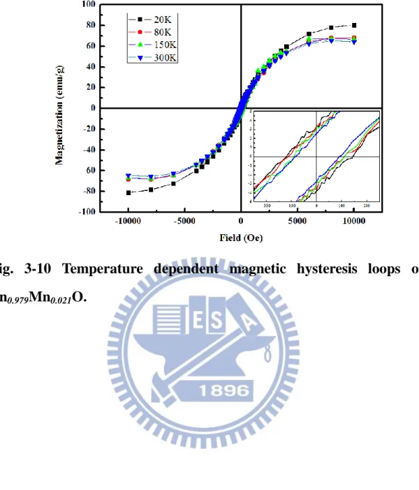
Fig.3-10 shows the temperature dependent magnetic hysteresis loops of Zn0.979Mn0.021O up to 300K. This implies the Curie temperature is
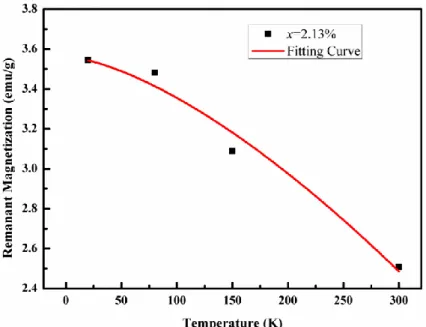
higher than 300K. Fig.3-11 shows the temperature dependent remanant magnetization. The spontaneous magnetization formula [32],
3 2 0(1 ( ) ) c T M M T ,
was used to calculate the Curie temperature. Where, M0 is the magnetization at T = 0K and Tc is the Curie temperature. The data is well
fitted by the formula and is shown by red line. The estimated Curie temperature is about 660K, which is certainly far above room temperature.
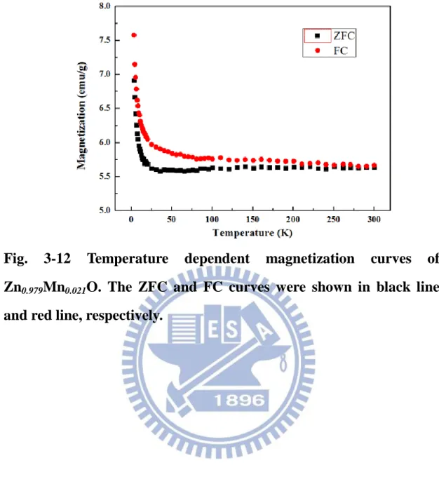
To further analyze the magnetic behaviors of ZnMnO samples, temperature dependent magnetization curves (M-T curves) of Zn0.979Mn0.021O were shown in Fig.3-12. In Fig.3-12, zero field cooling
(ZFC) and field cooling (FC) curves were shown. The curves were measured from 2K to 300K at applied magnetic field strength 200 Oe. The curves showed a clear divergence and the divergence persisted up to 300K, imply clear ferromagnetism at room temperature, which is consistent with previous results from hysteresis loops. However, in the region where temperature is below 50K, the curves show the paramagnetic behavior. We will discuss this behavior in more details later.
Fig.3-13 shows the hysteresis loops at room temperature with different Mn doping concentration. The data imply room temperature ferromagnetism of all samples including undoped ZnO sample.
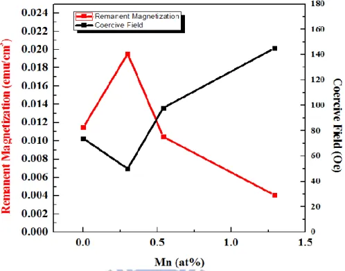
The ferromagnetism of undoped ZnO might contribute from the defect-induced bound magnetic polarons (BMP) [33] since carrier-mediated ferromagnetism required n-type or p-type doping. Moreover, the lowest Mn doping concentration (0.3%) has the highest remanent magnetization, but the remanent magnetization decreased as we increased the Mn doping concentration. The relationship between the remanent magnetization, coercive field and Mn doping concentration was shown in Fig.3-14. Besides, the remanent magnetization shows a negative correlation along with coercive field at different Mn doping concentration, it could be related to the motion of domain walls [34].
Here we assume the origin of magnetism in our samples contributed from the BMPs. The BMP model stated that the carriers trapped near defect centers would interact with localized spin moments, and the wavefunction of the localization carriers would extend to several nanometers, forming bound polarons. A polaron would exert antiferromagnetic exchange interaction on the spin moments e.g. magnetic ions, defect induced magnets which situate inside the polaron. Then the magnetic moments inside the polaron would become parallel aligned, e.g. forming ferromagnetism, to be in steady state [35]. Meanwhile, if there is a Mn2+ ion as next nearest neighbor for another Mn2+ ion, the two Mn2+ ions would experienced antiferromagnetic superexchange interaction, which favors anti-aligned spin configuration that could reduce the system energy to keep it in stable [36].
However, if the adjacent Mn2+ pair is inside a polaron, the antiferromagnetic exchange between the localized carrier and Mn2+ ions would lead to polarization of the polaron and contributes to
ferromagnetism, while the superexchange interaction between adjacent Mn2+ ions results in anti-aligned spin. The two interactions which favor different spin configuration would compete with each other and result in the decrease of the stability and overall magnetization of the BMP [37]. In our previous M-T curves, we showed the paramagnetic behavior dominates below 50K. The paramagnetic behavior could be attributed from the short-range antiferromagnetic exchange.
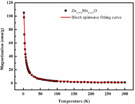
To further identify the exchange interaction strength between Mn2+ ions, Fig.3-15 shows the temperature dependent zero field cooling magnetization curve of Zn0.979Mn0.021O. The curve was well fitted by
Bloch spin wave function and Curie-Weiss law, implies the spontaneous magnetization exists, which is consistent with previous results from hysteresis loops. The fitting formula is as follows:[38]
3 2 0(1 ( ) ) c T c H M M T T ,
where M0 is the remanant magnetization at T=0, Tc is the Curie
temperature, c is the Curie constant, H is applied magnetic field and is the Weiss constant.
By Bloch spin wave function fitting, we can calculate a negative , which implies the existence of antiferromagnetic exchange interaction. Then we can further calculate the effective exchange constant (Jex) by the
following formula:[39]
2 1 3exB J x S S z k ,where x is the Mn doping concentration, S = 5/2 is the total spin quantum number of Mn2+ ion, z = 12 is the number of nearest neighbors for
cations.
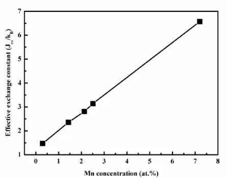
The relationship between the absolute value of Jex and Mn doping
concentration could be plot in Fig.3-16. The absolute value of Jex could
describe the antiferromagnetic exchange interaction strength. The absolute value of effective exchange increases with the Mn doping concentration. It implies the enhancement of antiferromagnetic exchange interaction, which corroborates with our previous assumption that the magnetization is due to polarization of Mn2+ ions induced by polaron.
The magnetization contribution of Mn ions can be estimated by hysteresis loops. For a divalent Mn ion, its 5 electrons in 3d orbital will align in parallel according to Hund’s rule, resulting in quantum numbers of s = 5/2, l = 0, and hence contribute to 5 effective Bohr magneton (B).
If we assume the remanent magnetization was contributed from ferromagnetic (FM) Mn ions and the saturated magnetization was contributed from the summation of ferromagnetic and paramagnetic (PM) Mn2+ ions. We could calculate the relative amount of FM and PM Mn ions, as shown in Fig. 3-17. The FM/PM ratios at different Mn doping concentration were shown in Fig. 3-18. The curves show the suppressed FM manganese ions at high Mn doping concentration which is due to the increasing anti-ferro-magnetic interaction in high Mn samples.
In summary, complicate magnetic phases coexisted in our samples, the magnetic polarons contributed to ferromagnetism whereas the antiferromagnetic superexchange interaction between Mn2+ ions and isolated Mn2+ ions contributed to antiferromagnetism or paramanetism, as shown in Fig.3-19.
Fig. 3-10 Temperature dependent magnetic hysteresis loops of Zn0.979Mn0.021O.
Fig. 3-11 Temperature dependent remanant magnetization of Zn0.979Mn0.021O. The spontaneous magnetization fitting is shown by
Fig. 3-12 Temperature dependent magnetization curves of Zn0.979Mn0.021O. The ZFC and FC curves were shown in black line
Fig. 3-13 Room temperature M-H curves of Zn1-xMnxO, where (a) x =
Fig. 3-14 Relationship between remanent magnetization (red line), coervice field (black line) and Mn doping concentration plot.
Fig. 3-15 Zero field cooling temperature dependent magnetization curves of Zn0.979Mn0.021O. The Bloch spin wave function fitting was
Fig. 3-16 The relationship between the effective exchange constant (Jex) and Mn doping concentration.
Fig. 3-17 Effective Bohr magneton contributed from ferromagnetic Mn ions (black points) and paramagnetic Mn ions (red points).
Fig. 3-18 Relative ratio of FM to PM Mn ions in different Mn doping concentration samples.
Fig. 3-19 Schematics of mixed magnetic phases in Zn1-xMnxO
Chapter 4 Conclusion
In this work, ZnMnO samples grown on Si(111) with AlN buffer layer by plasma-assisted molecular beam epitaxy with high optical quality were studied. The PL spectra show the strong excitonic emission, implies high quality of samples. The RRS phenomenon was enhanced in high Mn doping concentration ( x > 2.13%).
XAS provides the information about valence states of Mn ions in ZnMnO samples, Mn L-edge spectra indicate that most of Mn ions are divalent state and excluded the existence of Mn cluster. Room temperature hysteresis loops revealed RTFM of all samples including undoped ZnO. This magnetic phenomenon results from the existence of BMP. The Curie temperature was higher than 300K in all samples, but the remanent magnetization decreased with increasing Mn doping concentration due to the antiferromagnetic exchange interaction in the polarons.
References
[1] Mark Johnson and R. H. Silsbee, “Interfacial charge-spin coupling: Injection and detection of spin magnetization in metals”, Physical Review Letters 55 (17): 1790–1793 (1985).
[2] Supriyo Datta and Biswajit Das, “Electronic analog of the electrooptic modulator”, Applied Physics Letters 56 (7): 665–667 (1990).
[3] J. M. Kikkawa and D. D. Awschalom, “Resonant Spin Amplification in n-Type GaAs”, Physical Review Letters 80 (19): 4313 (1998).
[4] Xiaohua Lou, Christoph Adelmann, Scott A. Crooker, Eric S. Garlid, Jianjie Zhang, K. S. Madhukar Reddy, Soren D. Flexner, Chris J. Palmstrøm and Paul A. Crowell, “Electrical detection of spin transport in lateral ferromagnet–semiconductor devices”, Nature Physics 3 (3): 197-202 (2007).
[5] D. Chiba, M. Sawicki, Y. Nishitani, Y. Nakatani, F. Matsukura and H. Ohno, “Magnetization vector manipulation by electric fields”, Nature 455, 515-518 (2008).
[6] Gary A. Prinz, “Magnetoelectronics” Science 282, 1660 -1663 (1998). [7] G. Schmidt, D. Ferrand, L. W. Molemkamp, A. T. Filip, and B. J. Van Wees, “Fundamental obstacle for electrical spin injection from a ferromagnetic metal into a diffusive semiconductor”, Physical Review B
62, R4790-R4793 (2000)
[8] A. Fert and H. Jaffrès, “Conditions for efficient spin injection from a ferromagnetic metal into a semiconductor”, Physical Review B 64, 184420 (2001).
Goldman, “Differential conductance of the ferromagnet /superconductor interface of DyBa2Cu3O7/La2/3Ba1/3MnO3 heterostructures”, Applied Physics Letters, 73, 844 (2008).
[10] J. M. D. Coey and M. Venkatesan, “Half-metallic ferromagnetism: Example of CrO2”, Journal of Applied Physics 91 (10): 8345–8350 (2002).
[11] H. Ohno, “Making Nonmagnetic Semiconductors Ferromagnetic”, Science, 281 951-956 (1998).
[12] B. Beschoten, P. A. Crowell, I. Malajovich, D. D. Awschalom, F. Matsukura, A. Shen, and H. Ohno, “Magnetic Circular Dichroism Studies of Carrier-Induced Ferromagnetism in (Ga1-xMnx)As”, Physical Review Letters 83, 3073–3076 (1999).
[13] Jürgen König, Hsiu-Hau Lin, and Allan H. Mac Donald, “Theory of Diluted Magnetic Semiconductor Ferromagnetism”, Physical Review Letters 84, 5628–5631 (2000)
[14] T. Dietl, H. Ohno, F. Matsukura, J. Cibert, D. Ferrand, “Zener Model Description of Ferromagnetism in Zinc-Blende Magnetic Semiconductors”, Science 287 (5455): 1019-1022 (2000).
[15] D. Cherns and C. G. Jiao, “Electron Holography Studies of the Charge on Dislocations in GaN”, Physical Review Letters 87, 205504 (2001).
[16] W. H. Sun, S. J. Chua, L. S. Wang, and X. H. Zhang, “Outgoing multiphonon resonant Raman scattering and luminescence in Be- and C-implanted GaN”, Journal of Applied Physics 91, 4917 (2002).
[17] X. B. Zhang, T. Taliercio, S. Kolliakos and P. Lefebvre, “Influence of electron-phonon interaction on the optical properties of III nitride
semiconductors”, Journal of Physics: Condensed Matter 13, 7053 (2001). [18] A. Singhal, “Study of hydrogenation versus de-loading of Co and Mn doped ZnO semiconductor”, Journal of Alloys and Compounds 507, 312–316 (2010).
[19] U. Philipose, Selvakumar V. Nair, Simon Trudel, C. F. de Souza, S. Aouba, Ross H. Hill, and Harry E. Ruda, “High-temperature ferromagnetism in Mn-doped ZnO nanowires”, Applied Physics Letters
88, 263101 (2006).
[20] K. Masuko, A. Ashida, T. Yoshimura, and N. Fujimura, “Influence of antiferromagnetic exchange interaction on magnetic properties of ZnMnO thin films grown pseudomorphically on ZnO (000 1 ) single-crystal substrates”, Journal of Applied Physics 103, 043714 (2008).
[21] A. Ben Mahmoud, H. J. von Bardeleben, J. L. Cantin, E. Chikoidze, Y. Dumont, and A. Mauger, “Exchange interactions between magnetic ions and free carriers in ZnMnO: An electron paramagnetic resonance analysis”, Journal of Applied Physics 101, 09H102 (2007).
[22] Chang-Feng Yu, Tzu-Jen Lin, Shih-Jye Sun and Hsiung Chou, “Origin of ferromagnetism in nitrogen embedded ZnO : N thin films”, Journal of Physics D: Applied Physics 40, 6497-6500 (2007).
[23] Qingyu Xu, Heidemarie Schmidt, Shengqiang Zhou, Kay Potzger, Manfred Helm, Holger Hochmuth, Michael Lorenz, Annette Setzer, Pablo Esquinazi, Christoph Meinecke, and Marius Grundmann, “Room temperature ferromagnetism in ZnO films due to defects”, Applied Physics Letters 92, 082508 (2008).
Hochmuth, M. Grundmann, D. Spemann, T. Butz, G. Brauer, W. Anwand, G. Fischer, W. A. Adeagbo, W. Hergert, and A. Ernst, “Defect-induced magnetic order in pure ZnO films”, Physical Review B 80, 035331 (2009).
[25] Y. P. Varshni, “Temperature dependence of the energy gap in semiconductors”, Physica 34, 149 (1967).
[26] I. Sarkar, M. K. Sanyal, S. Takeyama, S. Kar, H. Hirayama, H. Mino, F. Komori, and S. Biswas, “Suppression of Mn photoluminescence in ferromagnetic state of Mn-doped ZnS nanocrystals”, Physical Review B
79, 054410 (2009).
[27] M. F. Cerqueira, M. I. Vasilevskiy, F. Oliveira, A. G. Rolo, T. Viseu, J. Ayres de Campos, E. Alves and R. Correia, “Resonant Raman scattering in ZnO:Mn and ZnO:Mn:Al thin films grown by RF sputtering”, Journal of Physics: Condensed Matter 23, 334205 (2011).
[28] Hsin-Ming Cheng, Kuo-Feng Lin, Hsu-Cheng, Chih-Jen Lin, Li-Jiaun Lin, and Wen-Feng Hsieh, “Enhanced Resonant Raman Scattering and Electron−Phonon Coupling from Self-Assembled Secondary ZnO Nanoparticles”, The Journal of Physical Chemistry B 109, 18385 (2005).
[29] The Long Phan, Roger Vincent, David Cherns, Nguyen Xuan Nghia and V. V. Ursaki, “Raman scattering in Me-doped ZnO nanorods (Me = Mn, Co, Cu and Ni) prepared by thermal diffusion”, Nanotechnology 19, 475702 (2008).
[30] C. W. M. Castleton and M. Altarelli, “Orbital ordering in the manganites: Resonant x-ray scattering predictions at the manganese LII and LIII edges”, Physical Review B 62, 1033-1038 (2000).
[31] Philip Coppens and James E. Penner-Hahn, “X-rays in Chemistry” (2001).
[32] Neil W. Ashcroft, N. David Mermin, “Solid State Physics” (1976). [33] Aurab Chakrabarty and Charles H. Patterson, “Defect-trapped electrons and ferromagnetic exchange in ZnO”, Physical Review B 84, 054441 (2011).
[34] Y.-P. Zhao, R. M. Gamache, G.-C. Wang, T. M. Lu, G. Palasantzas, and J. Th. M. De Hosson, “Effect of surface roughness on magnetic domain wall thickness, domain size, and coercivity”, Journal of Applied Physics 89, 1325 (2001).
[35] Masakatsu Umehara, “Theory for the bound magnetic polaron in diluted magnetic semiconductors by a modified molecular-field approximation”, Physical Review B 61, 12209–12215 (2000).
[36] P. W. Anderson, “Antiferromagnetism. Theory of Superexchange Interaction”, Physical Review 79, 350–356 (1950).
[37] P. A. Wolff, R. N. Bhatt and A. C. Durst, “Polaron ‐ polaron interactions in diluted magnetic semiconductors”, Journal of Applied Physics 79, 5196 (1996).
[38] N. Lenge, H. Kronmüller, “Low Temperature Magnetization of Sputtered Amorphous Fe-Xi-B Films”, physica status solidi (a) 95, 621 (1986).
[39] J. Spa